


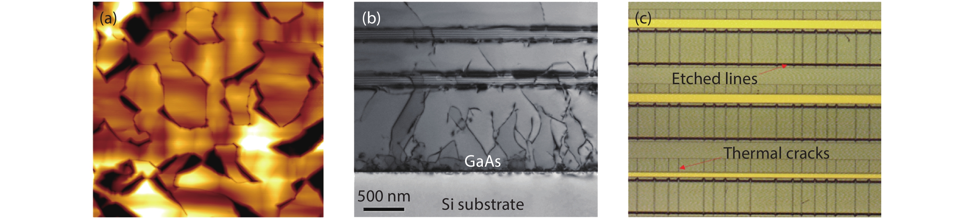
Fig. 1.
(Color online) Three major issues faced in monolithic III–V/Si integration: (a) APBs, (b) TDs and (c) thermal cracks.
REVIEWS
Shujie Pan, Victoria Cao, Mengya Liao, Ying Lu, Zizhuo Liu, Mingchu Tang, Siming Chen, Alwyn Seeds and Huiyun Liu
Corresponding author: Siming Chen, Email: siming.chen@ucl.ac.uk
Abstract: In the past few decades, numerous high-performance silicon (Si) photonic devices have been demonstrated. Si, as a photonic platform, has received renewed interest in recent years. Efficient Si-based III–V quantum-dot (QDs) lasers have long been a goal for semiconductor scientists because of the incomparable optical properties of III–V compounds. Although the material dissimilarity between III–V material and Si hindered the development of monolithic integrations for over 30 years, considerable breakthroughs happened in the 2000s. In this paper, we review recent progress in the epitaxial growth of various III–V QD lasers on both offcut Si substrate and on-axis Si (001) substrate. In addition, the fundamental challenges in monolithic growth will be explained together with the superior characteristics of QDs.
Keywords: quantum dots, silicon photonics, epitaxial growth, semiconductor laser
| [1] |
Reed G T, Mashanovich G, Gardes F Y, et al. Silicon optical modulators. Nat Photonics, 2010, 4, 518 doi: 10.1038/nphoton.2010.179
|
| [2] |
Xiao X, Xu H, Li X Y, et al. High-speed, low-loss silicon Mach–Zehnder modulators with doping optimization. Opt Express, 2013, 21, 4116 doi: 10.1364/OE.21.004116
|
| [3] |
Streshinsky M, Ding R, Liu Y, et al. Low power 50 Gb/s silicon traveling wave Mach-Zehnder modulator near 1300 nm. Opt Express, 2013, 21, 30350 doi: 10.1364/OE.21.030350
|
| [4] |
Dosunmu O I, Can D D, Emsley M K, et al. High-speed resonant cavity enhanced Ge photodetectors on reflecting Si substrates for 1550-nm operation. IEEE Photonics Technol Lett, 2005, 17, 175 doi: 10.1109/LPT.2004.836917
|
| [5] |
Yin T, Cohen R, Morse M M, et al. 31 GHz Ge n–i–p waveguide photodetectors on silicon-on-insulator substrate. Opt Express, 2007, 15, 13965 doi: 10.1364/OE.15.013965
|
| [6] |
Vivien L, Polzer A, Marris-Morini D, et al. Zero-bias 40 Gbit/s germanium waveguide photodetector on silicon. Opt Express, 2012, 20, 1096 doi: 10.1364/OE.20.001096
|
| [7] |
Bauters J F, Davenport M L, Heck M J R,et al. Silicon on ultra-low-loss waveguide photonic integration platform. Opt Express, 2013, 21, 544 doi: 10.1364/OE.21.000544
|
| [8] |
Heck M J R, Bauters J F, Davenport M L, et al. Ultra-low loss waveguide platform and its integration with silicon photonics. Laser Photon Rev, 2014, 8, 667 doi: 10.1002/lpor.201300183
|
| [9] |
Liu H Y, Wang T, Jiang Q, et al. Long-wavelength InAs/GaAs quantum-dot laser diode monolithically grown on Ge substrate. Nat Photonics, 2011, 5, 416 doi: 10.1038/nphoton.2011.120
|
| [10] |
Liang D, Bowers J E. Recent progress in lasers on silicon. Nat Photonics, 2010, 4, 511 doi: 10.1038/nphoton.2010.167
|
| [11] |
Chen S, et al. Electrically pumped continuous-wave III–V quantum dot lasers on silicon. Nat Photonics, 2016, 10, 307 doi: 10.1038/nphoton.2016.21
|
| [12] |
Tanabe K, Watanabe K, Arakawa Y. III–V/Si hybrid photonic devices by direct fusion bonding. Sci Rep, 2012, 2349 doi: 10.1038/srep00349
|
| [13] |
Tournié E, Cerutti L, Rodriguez J B, et al. Metamorphic III–V semiconductor lasers grown on silicon. MRS Bull, 2016, 41, 218 doi: 10.1557/mrs.2016.24
|
| [14] |
Fischer R, Masselink W T, Klem J, et al. Growth and properties of GaAs/AlGaAs on nonpolar substrates using molecular beam epitaxy. J Appl Phys, 1985, 58, 374 doi: 10.1063/1.335687
|
| [15] |
Wang W I. Molecular beam epitaxial growth and material properties of GaAs and AlGaAs on Si (100). J Appl Phys, 1984, 44, 1149 doi: 10.1063/1.94673
|
| [16] |
Li Q, Lau M. Epitaxial growth of highly mismatched III–V materials on (001) silicon for electronics and optoelectronics. Prog Cryst Growth Charact Mater, 2017, 63, 105 doi: 10.1016/j.pcrysgrow.2017.10.001
|
| [17] |
Alcotte R, Martin M, Moeyaert J, et al. Epitaxial growth of antiphase boundary free GaAs layer on 300 mm Si(001) substrate by metalorganic chemical vapour deposition with high mobility. APL Mater, 2016, 4, 46101 doi: 10.1063/1.4945586
|
| [18] |
Akiyama M, Kawarada Y, Kaminishi K. Growth of single domain gaas layer on (100)-oriented Si substrate by MOCVD. Jpn J Appl Phys, 1984, 23, L843 doi: 10.1143/JJAP.23.L843
|
| [19] |
Norman J C, Jung D, Wan Y, et al. Perspective: The future of quantum dot photonic integrated circuits. APL Photonics, 2018, 3, 30901 doi: 10.1063/1.5021345
|
| [20] |
Wu J, Chen S, Seeds A, et al. Quantum dot optoelectronic devices: lasers, photodetectors and solar cells. J Phys D, 2015, 48, 363001 doi: 10.1088/0022-3727/48/36/363001
|
| [21] |
Ueda O, Pearton S J. Materials and reliability handbook for semiconductor optical and electron devices. Springer, 2013
|
| [22] |
Kroemer H. A proposed class of hetero-junction injection lasers. Proc IEEE, 1963, 51, 1782
|
| [23] |
Alferov Z I. AlAs–GaAs heterojunction injection lasers with a low room-temperature threshold. Sov Phys Semicond, 1970, 3, 1107
|
| [24] |
Dingle R, Wiegmann W, Henry C H. Quantum states of confined carriers in very thin AlxGa1–xAs–GaAs–AlxGa1–xAs heterostructures. Dordrecht: Springer, 1988, 173
|
| [25] |
Kapon E, Simhony S, Bhat R, et al. Single quantum wire semiconductor lasers. Appl Phys Lett, 1989, 55, 2715 doi: 10.1063/1.101934
|
| [26] |
Arakawa Y, Sakaki H. Multidimensional quantum well laser and temperature dependence of its threshold current. Appl Phys Lett, 1982, 40, 939 doi: 10.1063/1.92959
|
| [27] |
Kirstaedter N, Ledentsov N N, Grundmann M, et al. Low threshold, large To injection laser emission from (InGa)As quantum dots. Electron Lett, 1994, 30, 1416 doi: 10.1049/el:19940939
|
| [28] |
Nishi K, Takemasa K, Sugawara M, et al. Development of quantum dot lasers for data-com and silicon photonics applications. IEEE J Sel Top Quantum Electron, 2017, 23, 1 doi: 10.1109/JSTQE.2017.2699787
|
| [29] |
Nishi K, Kageyama T, Yamaguchi M, et al. Molecular beam epitaxial growths of high-optical-gain InAs quantum dots on GaAs for long-wavelength emission. J Cryst Growth, 2013, 378, 459 doi: 10.1016/j.jcrysgro.2012.12.046
|
| [30] |
Ilahi B, Souaf M, Baira M, et al. Evolution of InAs/GaAs QDs size with the growth rate: a numerical investigation. J Nanomater, 2015, 2015, 1 doi: 10.1155/2015/847018
|
| [31] |
Leonard D, Fafard S, Pond K, et al. Structural and optical properties of self-assembled InGaAs quantum dots. J Vac Sci Technol B, 1994, 12, 2516 doi: 10.1116/1.587794
|
| [32] |
Nishi K, Saito H, Sugou S, et al. A narrow photoluminescence linewidth of 21 meV at 1.35 μm from strain-reduced InAs quantum dots covered by In0.2Ga0.8As grown on GaAs substrates. Appl Phys Lett, 1999, 74, 1111 doi: 10.1063/1.123459
|
| [33] |
Otsubo K, Hatori N, Ishida M, et al. Temperature-insensitive eye-opening under 10-Gb/s modulation of 1.3-μm P-doped quantum-dot lasers without current adjustments. Jpn J Appl Phys, 2004, 43, L1124 doi: 10.1143/JJAP.43.L1124
|
| [34] |
Takada K, Tanaka Y, Matsumoto T, et al. Wide-temperature-range 10.3 Gbit/s operations of 1.3 μm high-density quantum-dot DFB lasers. Electron Lett, 2011, 47, 206 doi: 10.1049/el.2010.3312
|
| [35] |
CapuaA, et al. Direct correlation between a highly damped modulation response and ultra low relative intensity noise in an InAs/GaAs quantum dot laser. Opt Express, 2007, 15, 5388 doi: 10.1364/OE.15.005388
|
| [36] |
Jung D, Zhang Z, Norman J, et al. Highly reliable low-threshold inas quantum dot lasers on on-axis (001) Si with 87% injection efficiency. ACS Photonics, 2018, 5, 1094 doi: 10.1021/acsphotonics.7b01387
|
| [37] |
Ovid’ko I. Relaxation mechanisms in strained nanoislands. Phys Rev Lett, 2002, 88, 46103 doi: 10.1103/PhysRevLett.88.046103
|
| [38] |
Tillmann K, Förster A. Critical dimensions for the formation of interfacial misfit dislocations of In0.6Ga0.4As islands on GaAs(001). Thin Solid Films, 2000, 368, 93 doi: 10.1016/S0040-6090(00)00858-0
|
| [39] |
Mi Z, Yang J, Bhattacharya P, et al. High-performance quantum dot lasers and integrated optoelectronics on Si. Proc IEEE, 2009, 97, 1239 doi: 10.1109/JPROC.2009.2014780
|
| [40] |
Shi B, Li Q, Lau K M. Self-organized InAs/InAlGaAs quantum dots as dislocation filters for InP films on (001) Si. J Cryst Growth, 2017, 464, 28 doi: 10.1016/j.jcrysgro.2016.10.089
|
| [41] |
Linder K, Phillips J, Qasaimeh O, et al. Self-organized In0.4Ga0.6As quantum-dot lasers grown on Si substrates. Appl Phys Lett, 1999, 70(10), 1355 doi: 10.1063/1.123548
|
| [42] |
Wang T, Liu H, Lee A, et al. 1.3-μm InAs/GaAs quantum-dot lasers monolithically grown on Si substrates. Opt Express, 2011, 19, 11381 doi: 10.1364/OE.19.011381
|
| [43] |
Lee A D, Jiang Q, Tang M C, et al. InAs/GaAs quantum-dot lasers monolithically grown on Si, Ge, and Ge-on-Si substrates. IEEE J Sel Top Quantum Electron, 2013, 19, 1901107 doi: 10.1109/JSTQE.2013.2247979
|
| [44] |
Chen S M, Tang M, Wu J, et al. 1.3-μm InAs/GaAs quantum-dot lasers monolithically grown on Si substrates using InAlAs/GaAs dislocation filter layers. Opt Express, 2014, 22, 11528 doi: 10.1364/OE.22.011528
|
| [45] |
Orchard J R, Shutts S, Sobiesierski A, et al. In situ annealing enhancement of the optical properties and laser device performance of InAs quantum dots grown on Si substrates. Opt Express, 2016, 24, 6196 doi: 10.1364/OE.24.006196
|
| [46] |
Jiang Q, Tang M C, Wu J, et al. 1.3 μm InAs/GaAs quantum-dot laser monolithically grown on Si substrates operating over 100 °C. Electron Lett, 2014, 50, 1467 doi: 10.1049/el.2014.2414
|
| [47] |
Liao M, Chen S, Park J S, et al. III–V quantum-dot lasers monolithically grown on silicon. Semicond Sci Technol, 2018, 33, 123002 doi: 10.1088/1361-6641/aae6a5
|
| [48] |
Tang M, Chen S M, Wu J, et al. Optimizations of defect filter layers for 1.3-μm InAs/GaAs quantum-dot lasers monolithically grown on Si substrates. IEEE J Sel Top Quantum Electron, 2016, 22, 50 doi: 10.1109/JSTQE.2016.2551941
|
| [49] |
Liao M, Chen S M, Liu Z X, et al. Low-noise 13 μm InAs/GaAs quantum dot laser monolithically grown on silicon. Photonics Res, 2018, 6, 1062 doi: 10.1364/PRJ.6.001062
|
| [50] |
Hantschmann C, Vasil'ev P P, Chen S M, et al. Gain switching of monolithic 1.3 μm InAs/GaAs quantum dot lasers on silicon. J Light Technol, 2018, 36, 3837 doi: 10.1109/JLT.2018.2851918
|
| [51] |
Hantschmann C, Vasil’ev P P, Wonfor A, et al. Understanding the bandwidth limitations in monolithic 1.3 μm InAs/GaAs quantum dot lasers on silicon. J Light Technol, 2019, 37, 949 doi: 10.1109/JLT.2018.2884025
|
| [52] |
Agrawal G P. Fiber-optic communication systems. Wiley, 2013
|
| [53] |
Merckling C, Waldron N, Jiang S, et al. Heteroepitaxy of InP on Si(001) by selective-area metal organic vapor-phase epitaxy in sub-50 nm width trenches: The role of the nucleation layer and the recess engineering. J Appl Phys, 2014, 115, 23710 doi: 10.1063/1.4862044
|
| [54] |
Wang Z, Tian B, Pantouvaki M, et al. Room-temperature InP distributed feedback laser array directly grown on silicon. Nat Photonics, 2015, 9, 837 doi: 10.1038/nphoton.2015.199
|
| [55] |
Tian B, Wang Z C, Pantouvaki M, et al. Room temperature O-band DFB laser array directly grown on (001) silicon. Nano Lett, 2017, 17, 559 doi: 10.1021/acs.nanolett.6b04690
|
| [56] |
Wang Y, Chen S M, Yu Y, et al. Monolithic quantum-dot distributed feedback laser array on silicon. Optica, 2018, 5, 528 doi: 10.1364/OPTICA.5.000528
|
| [57] |
Kim H C, Wiedmann J, Matsui K, et al. 1.5-μm-wavelength distributed feedback lasers with deeply etched first-order vertical grating. Jpn J Appl Phys, 2001, 40, L1107 doi: 10.1143/JJAP.40.L1107
|
| [58] |
Vahala K J. Optical microcavities. Nature, 2003, 424, 839 doi: 10.1038/nature01939
|
| [59] |
Maximov M V, Kryzhanovskaya N V, Nadtochiy A M, et al. Ultrasmall microdisk and microring lasers based on InAs/InGaAs/GaAs quantum dots. Nanoscale Res Lett, 2014, 9, 657 doi: 10.1186/1556-276X-9-657
|
| [60] |
Kryzhanovskaya N V, Zhukov A Z, Maximov M V, et al. Room temperature lasing in 1-μm microdisk quantum dot lasers. IEEE J Sel Top Quantum Electron, 2015, 21, 709 doi: 10.1109/JSTQE.2015.2439156
|
| [61] |
Kryzhanovskaya N, Zhukov A E, Maximov M V, et al. Heat-sink free CW operation of injection microdisk lasers grown on Si substrate with emission wavelength beyond 13 μm. Opt Lett, 2017, 42, 3319 doi: 10.1364/OL.42.003319
|
| [62] |
Kryzhanovskaya N, Moiseev E, Polubavkina Y, et al. Elevated temperature lasing from injection microdisk lasers on silicon. Laser Phys Lett, 2018, 15, 15802 doi: 10.1088/1612-202X/aa9306
|
| [63] |
Volz K, Beyer A, Witte W, et al. GaP-nucleation on exact Si (001) substrates for III/V device integration. J Cryst Growth, 2011, 315, 37 doi: 10.1016/j.jcrysgro.2010.10.036
|
| [64] |
Liu A Y, Peters J, Huang X, et al. Electrically pumped continuous-wave 13 μm quantum-dot lasers epitaxially grown on on-axis (001) GaP/Si. Opt Lett, 2017, 42, 338 doi: 10.1364/OL.42.000338
|
| [65] |
Jung D, Song Y, Lee M, et al. InGaAs/GaAs quantum well lasers grown on exact GaP/Si (001). Electron Lett, 2014, 50, 1226 doi: 10.1049/el.2014.2077
|
| [66] |
Li Q, Ng K W, Lau K M. Growing antiphase-domain-free GaAs thin films out of highly ordered planar nanowire arrays on exact (001) silicon. Appl Phys Lett, 2015, 106, 72105 doi: 10.1063/1.4913432
|
| [67] |
Li Q, Wan Y T, Liu A Y, et al. 13-μm InAs quantum-dot micro-disk lasers on V-groove patterned and unpatterned (001) silicon. Opt Express, 2016, 24, 21038 doi: 10.1364/OE.24.021038
|
| [68] |
Chen S M, Liao M Y, Tang M C, et al. Electrically pumped continuous-wave 1.3 μm InAs/GaAs quantum dot lasers monolithically grown on on-axis Si (001) substrates. Opt Express, 2017, 25, 4632 doi: 10.1364/OE.25.004632
|
| [69] |
Li K, Liu Z, Tang M, et al. O-band InAs/GaAs quantum dot laser monolithically integrated on exact (001) Si substrate. J Cryst Growth, 2019, 511, 56 doi: 10.1016/j.jcrysgro.2019.01.016
|
| [70] |
Zhou T J, Tang M C, Xiang G H, et al. Ultra-low threshold InAs/GaAs quantum dot microdisk lasers on planar on-axis Si (001) substrates. Optica, 2019, 6, 430 doi: 10.1364/OPTICA.6.000430
|


Article views: 6499 Times PDF downloads: 216 Times Cited by: 0 Times
Received: 29 June 2019 Revised: 27 July 2019 Online: Uncorrected proof: 03 September 2019Accepted Manuscript: 03 September 2019Published: 01 October 2019
| Citation: |
Shujie Pan, Victoria Cao, Mengya Liao, Ying Lu, Zizhuo Liu, Mingchu Tang, Siming Chen, Alwyn Seeds, Huiyun Liu. Recent progress in epitaxial growth of III–V quantum-dot lasers on silicon substrate[J]. Journal of Semiconductors, 2019, 40(10): 101302. doi: 10.1088/1674-4926/40/10/101302
****
S J Pan, V Cao, M Y Liao, Y Lu, Z Z Liu, M C Tang, S M Chen, A Seeds, H Y Liu, Recent progress in epitaxial growth of III–V quantum-dot lasers on silicon substrate[J]. J. Semicond., 2019, 40(10): 101302. doi: 10.1088/1674-4926/40/10/101302.

|
| [1] |
Reed G T, Mashanovich G, Gardes F Y, et al. Silicon optical modulators. Nat Photonics, 2010, 4, 518 doi: 10.1038/nphoton.2010.179
|
| [2] |
Xiao X, Xu H, Li X Y, et al. High-speed, low-loss silicon Mach–Zehnder modulators with doping optimization. Opt Express, 2013, 21, 4116 doi: 10.1364/OE.21.004116
|
| [3] |
Streshinsky M, Ding R, Liu Y, et al. Low power 50 Gb/s silicon traveling wave Mach-Zehnder modulator near 1300 nm. Opt Express, 2013, 21, 30350 doi: 10.1364/OE.21.030350
|
| [4] |
Dosunmu O I, Can D D, Emsley M K, et al. High-speed resonant cavity enhanced Ge photodetectors on reflecting Si substrates for 1550-nm operation. IEEE Photonics Technol Lett, 2005, 17, 175 doi: 10.1109/LPT.2004.836917
|
| [5] |
Yin T, Cohen R, Morse M M, et al. 31 GHz Ge n–i–p waveguide photodetectors on silicon-on-insulator substrate. Opt Express, 2007, 15, 13965 doi: 10.1364/OE.15.013965
|
| [6] |
Vivien L, Polzer A, Marris-Morini D, et al. Zero-bias 40 Gbit/s germanium waveguide photodetector on silicon. Opt Express, 2012, 20, 1096 doi: 10.1364/OE.20.001096
|
| [7] |
Bauters J F, Davenport M L, Heck M J R,et al. Silicon on ultra-low-loss waveguide photonic integration platform. Opt Express, 2013, 21, 544 doi: 10.1364/OE.21.000544
|
| [8] |
Heck M J R, Bauters J F, Davenport M L, et al. Ultra-low loss waveguide platform and its integration with silicon photonics. Laser Photon Rev, 2014, 8, 667 doi: 10.1002/lpor.201300183
|
| [9] |
Liu H Y, Wang T, Jiang Q, et al. Long-wavelength InAs/GaAs quantum-dot laser diode monolithically grown on Ge substrate. Nat Photonics, 2011, 5, 416 doi: 10.1038/nphoton.2011.120
|
| [10] |
Liang D, Bowers J E. Recent progress in lasers on silicon. Nat Photonics, 2010, 4, 511 doi: 10.1038/nphoton.2010.167
|
| [11] |
Chen S, et al. Electrically pumped continuous-wave III–V quantum dot lasers on silicon. Nat Photonics, 2016, 10, 307 doi: 10.1038/nphoton.2016.21
|
| [12] |
Tanabe K, Watanabe K, Arakawa Y. III–V/Si hybrid photonic devices by direct fusion bonding. Sci Rep, 2012, 2349 doi: 10.1038/srep00349
|
| [13] |
Tournié E, Cerutti L, Rodriguez J B, et al. Metamorphic III–V semiconductor lasers grown on silicon. MRS Bull, 2016, 41, 218 doi: 10.1557/mrs.2016.24
|
| [14] |
Fischer R, Masselink W T, Klem J, et al. Growth and properties of GaAs/AlGaAs on nonpolar substrates using molecular beam epitaxy. J Appl Phys, 1985, 58, 374 doi: 10.1063/1.335687
|
| [15] |
Wang W I. Molecular beam epitaxial growth and material properties of GaAs and AlGaAs on Si (100). J Appl Phys, 1984, 44, 1149 doi: 10.1063/1.94673
|
| [16] |
Li Q, Lau M. Epitaxial growth of highly mismatched III–V materials on (001) silicon for electronics and optoelectronics. Prog Cryst Growth Charact Mater, 2017, 63, 105 doi: 10.1016/j.pcrysgrow.2017.10.001
|
| [17] |
Alcotte R, Martin M, Moeyaert J, et al. Epitaxial growth of antiphase boundary free GaAs layer on 300 mm Si(001) substrate by metalorganic chemical vapour deposition with high mobility. APL Mater, 2016, 4, 46101 doi: 10.1063/1.4945586
|
| [18] |
Akiyama M, Kawarada Y, Kaminishi K. Growth of single domain gaas layer on (100)-oriented Si substrate by MOCVD. Jpn J Appl Phys, 1984, 23, L843 doi: 10.1143/JJAP.23.L843
|
| [19] |
Norman J C, Jung D, Wan Y, et al. Perspective: The future of quantum dot photonic integrated circuits. APL Photonics, 2018, 3, 30901 doi: 10.1063/1.5021345
|
| [20] |
Wu J, Chen S, Seeds A, et al. Quantum dot optoelectronic devices: lasers, photodetectors and solar cells. J Phys D, 2015, 48, 363001 doi: 10.1088/0022-3727/48/36/363001
|
| [21] |
Ueda O, Pearton S J. Materials and reliability handbook for semiconductor optical and electron devices. Springer, 2013
|
| [22] |
Kroemer H. A proposed class of hetero-junction injection lasers. Proc IEEE, 1963, 51, 1782
|
| [23] |
Alferov Z I. AlAs–GaAs heterojunction injection lasers with a low room-temperature threshold. Sov Phys Semicond, 1970, 3, 1107
|
| [24] |
Dingle R, Wiegmann W, Henry C H. Quantum states of confined carriers in very thin AlxGa1–xAs–GaAs–AlxGa1–xAs heterostructures. Dordrecht: Springer, 1988, 173
|
| [25] |
Kapon E, Simhony S, Bhat R, et al. Single quantum wire semiconductor lasers. Appl Phys Lett, 1989, 55, 2715 doi: 10.1063/1.101934
|
| [26] |
Arakawa Y, Sakaki H. Multidimensional quantum well laser and temperature dependence of its threshold current. Appl Phys Lett, 1982, 40, 939 doi: 10.1063/1.92959
|
| [27] |
Kirstaedter N, Ledentsov N N, Grundmann M, et al. Low threshold, large To injection laser emission from (InGa)As quantum dots. Electron Lett, 1994, 30, 1416 doi: 10.1049/el:19940939
|
| [28] |
Nishi K, Takemasa K, Sugawara M, et al. Development of quantum dot lasers for data-com and silicon photonics applications. IEEE J Sel Top Quantum Electron, 2017, 23, 1 doi: 10.1109/JSTQE.2017.2699787
|
| [29] |
Nishi K, Kageyama T, Yamaguchi M, et al. Molecular beam epitaxial growths of high-optical-gain InAs quantum dots on GaAs for long-wavelength emission. J Cryst Growth, 2013, 378, 459 doi: 10.1016/j.jcrysgro.2012.12.046
|
| [30] |
Ilahi B, Souaf M, Baira M, et al. Evolution of InAs/GaAs QDs size with the growth rate: a numerical investigation. J Nanomater, 2015, 2015, 1 doi: 10.1155/2015/847018
|
| [31] |
Leonard D, Fafard S, Pond K, et al. Structural and optical properties of self-assembled InGaAs quantum dots. J Vac Sci Technol B, 1994, 12, 2516 doi: 10.1116/1.587794
|
| [32] |
Nishi K, Saito H, Sugou S, et al. A narrow photoluminescence linewidth of 21 meV at 1.35 μm from strain-reduced InAs quantum dots covered by In0.2Ga0.8As grown on GaAs substrates. Appl Phys Lett, 1999, 74, 1111 doi: 10.1063/1.123459
|
| [33] |
Otsubo K, Hatori N, Ishida M, et al. Temperature-insensitive eye-opening under 10-Gb/s modulation of 1.3-μm P-doped quantum-dot lasers without current adjustments. Jpn J Appl Phys, 2004, 43, L1124 doi: 10.1143/JJAP.43.L1124
|
| [34] |
Takada K, Tanaka Y, Matsumoto T, et al. Wide-temperature-range 10.3 Gbit/s operations of 1.3 μm high-density quantum-dot DFB lasers. Electron Lett, 2011, 47, 206 doi: 10.1049/el.2010.3312
|
| [35] |
CapuaA, et al. Direct correlation between a highly damped modulation response and ultra low relative intensity noise in an InAs/GaAs quantum dot laser. Opt Express, 2007, 15, 5388 doi: 10.1364/OE.15.005388
|
| [36] |
Jung D, Zhang Z, Norman J, et al. Highly reliable low-threshold inas quantum dot lasers on on-axis (001) Si with 87% injection efficiency. ACS Photonics, 2018, 5, 1094 doi: 10.1021/acsphotonics.7b01387
|
| [37] |
Ovid’ko I. Relaxation mechanisms in strained nanoislands. Phys Rev Lett, 2002, 88, 46103 doi: 10.1103/PhysRevLett.88.046103
|
| [38] |
Tillmann K, Förster A. Critical dimensions for the formation of interfacial misfit dislocations of In0.6Ga0.4As islands on GaAs(001). Thin Solid Films, 2000, 368, 93 doi: 10.1016/S0040-6090(00)00858-0
|
| [39] |
Mi Z, Yang J, Bhattacharya P, et al. High-performance quantum dot lasers and integrated optoelectronics on Si. Proc IEEE, 2009, 97, 1239 doi: 10.1109/JPROC.2009.2014780
|
| [40] |
Shi B, Li Q, Lau K M. Self-organized InAs/InAlGaAs quantum dots as dislocation filters for InP films on (001) Si. J Cryst Growth, 2017, 464, 28 doi: 10.1016/j.jcrysgro.2016.10.089
|
| [41] |
Linder K, Phillips J, Qasaimeh O, et al. Self-organized In0.4Ga0.6As quantum-dot lasers grown on Si substrates. Appl Phys Lett, 1999, 70(10), 1355 doi: 10.1063/1.123548
|
| [42] |
Wang T, Liu H, Lee A, et al. 1.3-μm InAs/GaAs quantum-dot lasers monolithically grown on Si substrates. Opt Express, 2011, 19, 11381 doi: 10.1364/OE.19.011381
|
| [43] |
Lee A D, Jiang Q, Tang M C, et al. InAs/GaAs quantum-dot lasers monolithically grown on Si, Ge, and Ge-on-Si substrates. IEEE J Sel Top Quantum Electron, 2013, 19, 1901107 doi: 10.1109/JSTQE.2013.2247979
|
| [44] |
Chen S M, Tang M, Wu J, et al. 1.3-μm InAs/GaAs quantum-dot lasers monolithically grown on Si substrates using InAlAs/GaAs dislocation filter layers. Opt Express, 2014, 22, 11528 doi: 10.1364/OE.22.011528
|
| [45] |
Orchard J R, Shutts S, Sobiesierski A, et al. In situ annealing enhancement of the optical properties and laser device performance of InAs quantum dots grown on Si substrates. Opt Express, 2016, 24, 6196 doi: 10.1364/OE.24.006196
|
| [46] |
Jiang Q, Tang M C, Wu J, et al. 1.3 μm InAs/GaAs quantum-dot laser monolithically grown on Si substrates operating over 100 °C. Electron Lett, 2014, 50, 1467 doi: 10.1049/el.2014.2414
|
| [47] |
Liao M, Chen S, Park J S, et al. III–V quantum-dot lasers monolithically grown on silicon. Semicond Sci Technol, 2018, 33, 123002 doi: 10.1088/1361-6641/aae6a5
|
| [48] |
Tang M, Chen S M, Wu J, et al. Optimizations of defect filter layers for 1.3-μm InAs/GaAs quantum-dot lasers monolithically grown on Si substrates. IEEE J Sel Top Quantum Electron, 2016, 22, 50 doi: 10.1109/JSTQE.2016.2551941
|
| [49] |
Liao M, Chen S M, Liu Z X, et al. Low-noise 13 μm InAs/GaAs quantum dot laser monolithically grown on silicon. Photonics Res, 2018, 6, 1062 doi: 10.1364/PRJ.6.001062
|
| [50] |
Hantschmann C, Vasil'ev P P, Chen S M, et al. Gain switching of monolithic 1.3 μm InAs/GaAs quantum dot lasers on silicon. J Light Technol, 2018, 36, 3837 doi: 10.1109/JLT.2018.2851918
|
| [51] |
Hantschmann C, Vasil’ev P P, Wonfor A, et al. Understanding the bandwidth limitations in monolithic 1.3 μm InAs/GaAs quantum dot lasers on silicon. J Light Technol, 2019, 37, 949 doi: 10.1109/JLT.2018.2884025
|
| [52] |
Agrawal G P. Fiber-optic communication systems. Wiley, 2013
|
| [53] |
Merckling C, Waldron N, Jiang S, et al. Heteroepitaxy of InP on Si(001) by selective-area metal organic vapor-phase epitaxy in sub-50 nm width trenches: The role of the nucleation layer and the recess engineering. J Appl Phys, 2014, 115, 23710 doi: 10.1063/1.4862044
|
| [54] |
Wang Z, Tian B, Pantouvaki M, et al. Room-temperature InP distributed feedback laser array directly grown on silicon. Nat Photonics, 2015, 9, 837 doi: 10.1038/nphoton.2015.199
|
| [55] |
Tian B, Wang Z C, Pantouvaki M, et al. Room temperature O-band DFB laser array directly grown on (001) silicon. Nano Lett, 2017, 17, 559 doi: 10.1021/acs.nanolett.6b04690
|
| [56] |
Wang Y, Chen S M, Yu Y, et al. Monolithic quantum-dot distributed feedback laser array on silicon. Optica, 2018, 5, 528 doi: 10.1364/OPTICA.5.000528
|
| [57] |
Kim H C, Wiedmann J, Matsui K, et al. 1.5-μm-wavelength distributed feedback lasers with deeply etched first-order vertical grating. Jpn J Appl Phys, 2001, 40, L1107 doi: 10.1143/JJAP.40.L1107
|
| [58] |
Vahala K J. Optical microcavities. Nature, 2003, 424, 839 doi: 10.1038/nature01939
|
| [59] |
Maximov M V, Kryzhanovskaya N V, Nadtochiy A M, et al. Ultrasmall microdisk and microring lasers based on InAs/InGaAs/GaAs quantum dots. Nanoscale Res Lett, 2014, 9, 657 doi: 10.1186/1556-276X-9-657
|
| [60] |
Kryzhanovskaya N V, Zhukov A Z, Maximov M V, et al. Room temperature lasing in 1-μm microdisk quantum dot lasers. IEEE J Sel Top Quantum Electron, 2015, 21, 709 doi: 10.1109/JSTQE.2015.2439156
|
| [61] |
Kryzhanovskaya N, Zhukov A E, Maximov M V, et al. Heat-sink free CW operation of injection microdisk lasers grown on Si substrate with emission wavelength beyond 13 μm. Opt Lett, 2017, 42, 3319 doi: 10.1364/OL.42.003319
|
| [62] |
Kryzhanovskaya N, Moiseev E, Polubavkina Y, et al. Elevated temperature lasing from injection microdisk lasers on silicon. Laser Phys Lett, 2018, 15, 15802 doi: 10.1088/1612-202X/aa9306
|
| [63] |
Volz K, Beyer A, Witte W, et al. GaP-nucleation on exact Si (001) substrates for III/V device integration. J Cryst Growth, 2011, 315, 37 doi: 10.1016/j.jcrysgro.2010.10.036
|
| [64] |
Liu A Y, Peters J, Huang X, et al. Electrically pumped continuous-wave 13 μm quantum-dot lasers epitaxially grown on on-axis (001) GaP/Si. Opt Lett, 2017, 42, 338 doi: 10.1364/OL.42.000338
|
| [65] |
Jung D, Song Y, Lee M, et al. InGaAs/GaAs quantum well lasers grown on exact GaP/Si (001). Electron Lett, 2014, 50, 1226 doi: 10.1049/el.2014.2077
|
| [66] |
Li Q, Ng K W, Lau K M. Growing antiphase-domain-free GaAs thin films out of highly ordered planar nanowire arrays on exact (001) silicon. Appl Phys Lett, 2015, 106, 72105 doi: 10.1063/1.4913432
|
| [67] |
Li Q, Wan Y T, Liu A Y, et al. 13-μm InAs quantum-dot micro-disk lasers on V-groove patterned and unpatterned (001) silicon. Opt Express, 2016, 24, 21038 doi: 10.1364/OE.24.021038
|
| [68] |
Chen S M, Liao M Y, Tang M C, et al. Electrically pumped continuous-wave 1.3 μm InAs/GaAs quantum dot lasers monolithically grown on on-axis Si (001) substrates. Opt Express, 2017, 25, 4632 doi: 10.1364/OE.25.004632
|
| [69] |
Li K, Liu Z, Tang M, et al. O-band InAs/GaAs quantum dot laser monolithically integrated on exact (001) Si substrate. J Cryst Growth, 2019, 511, 56 doi: 10.1016/j.jcrysgro.2019.01.016
|
| [70] |
Zhou T J, Tang M C, Xiang G H, et al. Ultra-low threshold InAs/GaAs quantum dot microdisk lasers on planar on-axis Si (001) substrates. Optica, 2019, 6, 430 doi: 10.1364/OPTICA.6.000430
|

 WeChat ID
Journal of Semiconductors © 2017 All Rights Reserved 京ICP备05085259号-2

 DownLoad:

