


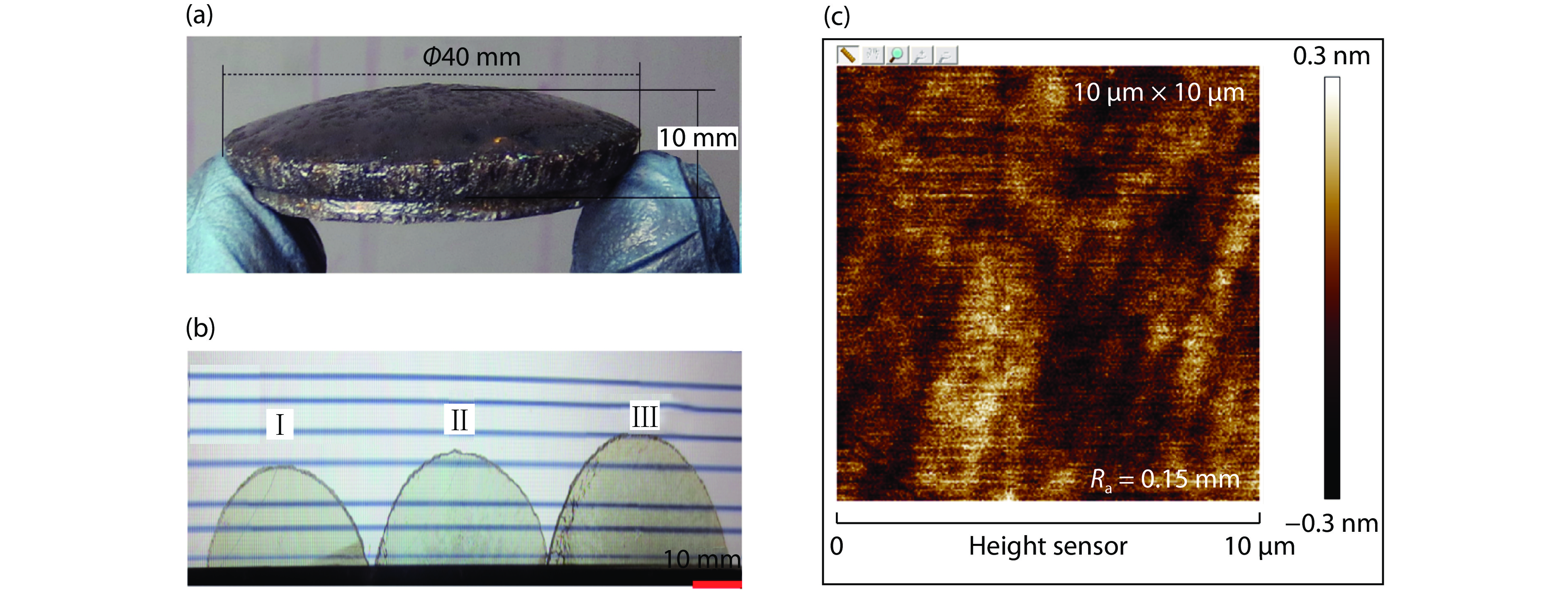
Fig. 1.
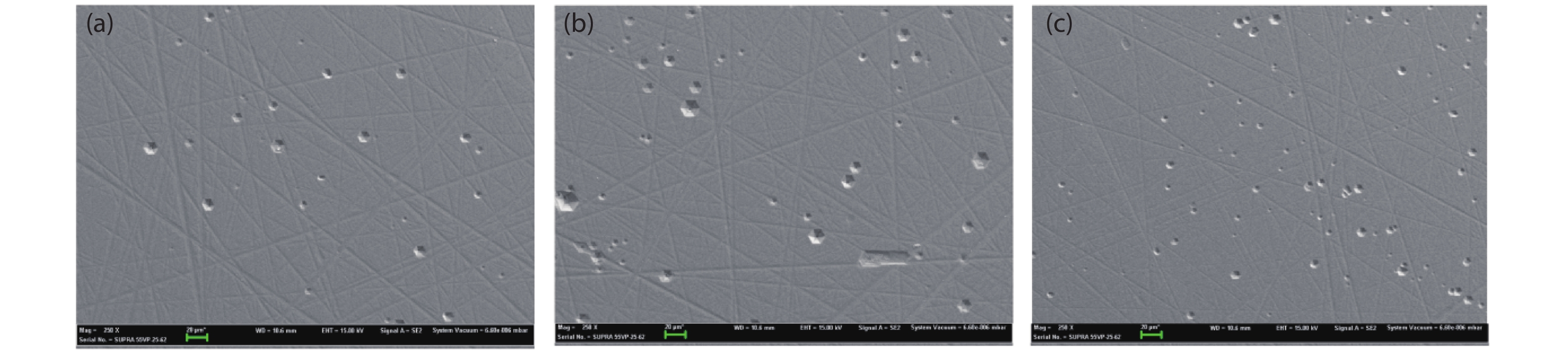
(Color online) (a) AlN single crystal. (b) AlN samples. (c) Ra of AlN sample at area of 10 × 10 μm2.
ARTICLES
Li Zhang, Haitao Qi, Hongjuan Cheng, Lei Jin and Yuezeng Shi
Corresponding author: Haitao Qi, Email: tjuqht1@163.com
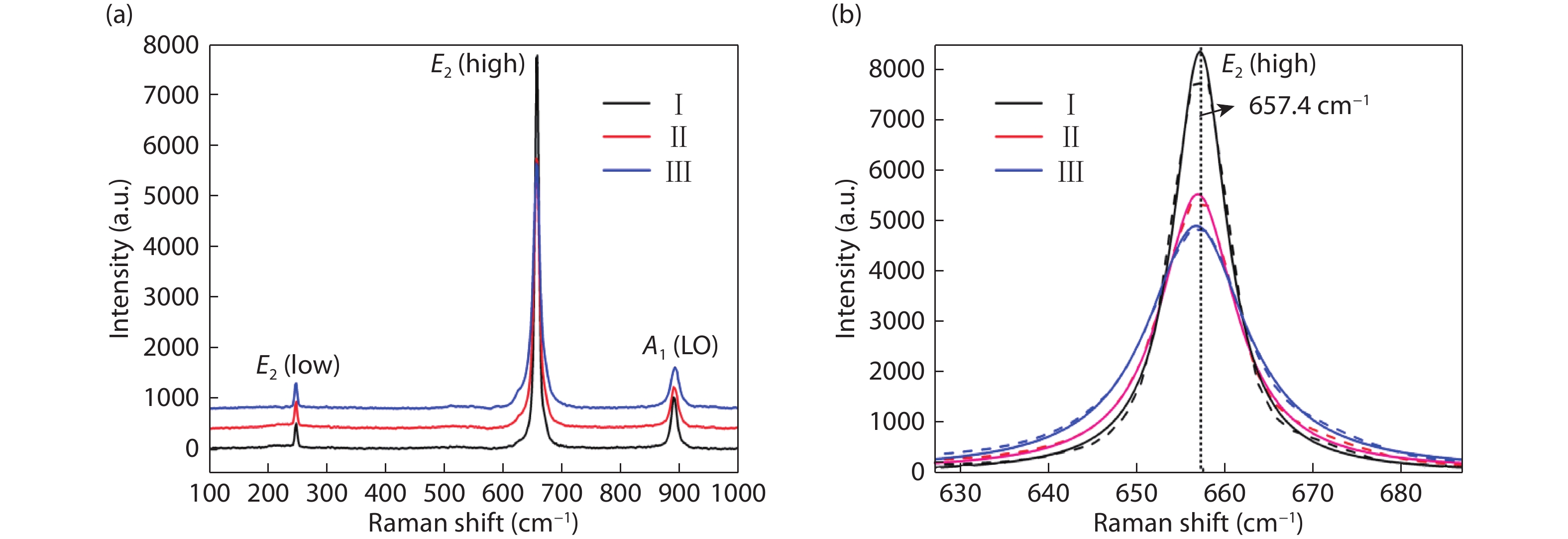
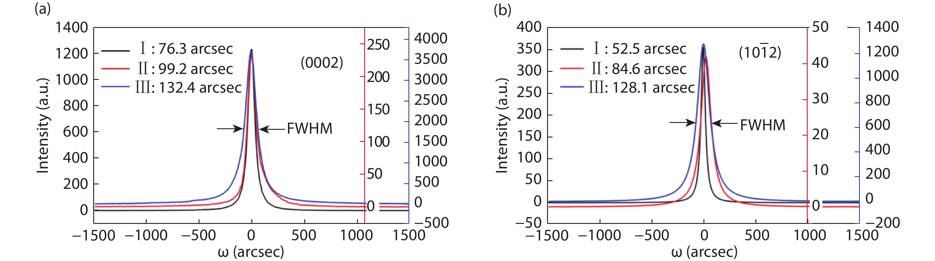
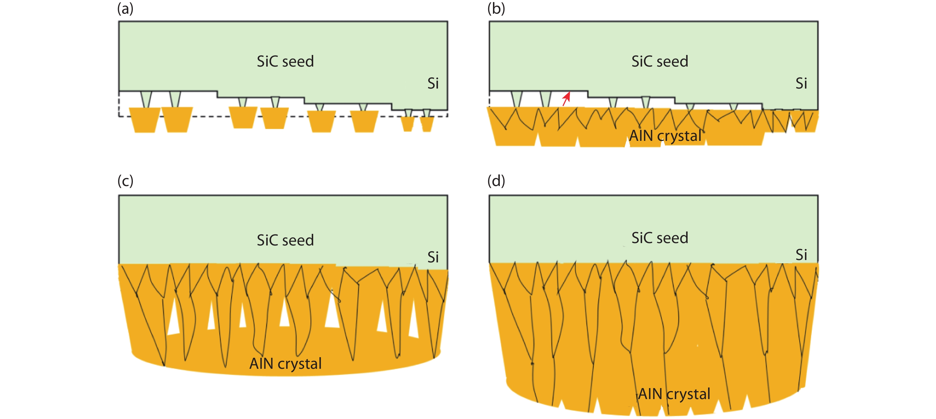
Abstract: Large size AlN bulk crystal has been grown on SiC heterogeneous seed by physical vapor transport (PVT). The properties of AlN wafer were characterized by high resolution X-ray diffraction (HRXRD), Raman spectroscopy, etched method and atomic force microscope (AFM). Growth mechanism of AlN crystal grown on heterogeneous SiC seeds was proposed. Crystallization quality of AlN samples were improved with the growth process, which is associated with the growth mechanism. AlN single wafer has excellent crystallization quality, which is indicated by HRXRD showing the (0002), (
Keywords: heterogeneous growth, AlN seeds, crystallization quality, characterization
| [1] |
Wang W J, Zuo S B, Bao H Q, et al. Effect of the seed crystallographic orientation on AlN bulk crystal growth by PVT method. Cryst Res Technol, 2011, 46(5), 455 doi: 10.1002/crat.201100035
|
| [2] |
http://www.cisuvc.com
|
| [3] |
http://www.hexatechinc.com
|
| [4] |
Epelbaum B M, Bickermann M, Winnacker A. Approaches to seeded PVT growth of AlN crystals. J Cryst Growth, 2005, 275, 479 doi: 10.1016/j.jcrysgro.2004.11.113
|
| [5] |
Hartmann C, Dittmar A, Wollweber J, et al. Bulk AlN growth by physical vapour transport. Semicond Sci Technol, 2014, 29, 084002 doi: 10.1088/0268-1242/29/8/084002
|
| [6] |
Hartmann C, Wollweber J, Dittmar A, et al. Preparation of bulk AlN seeds by spontaneous nucleation of freestanding crystals. Jpn J Appl Phys, 2013, 52, 08JA06 doi: 10.7567/JJAP.52.08JA06
|
| [7] |
Helava H I, Mokhov E N, Avdeev O A, et al. Growth of low-defect SiC and AlN crystals in refractory metal crucibles. Mater Sci Forum, 2013, 740–742, 85 doi: 10.4028/www.scientific.net/MSF.740-742.85
|
| [8] |
Sumathi R R, Paun M. Growth of (0001) AlN single crystals using carbon-face SiC as seeds. Mater Sci Forum, 2013, 740–742, 99 doi: 10.4028/www.scientific.net/msf.740-742.99
|
| [9] |
Sumathi R R, Gille P. Role of SiC substrate polarity on the growth and properties of bulk AlN single crystals. J Mater Sci: Mater Electron, 2014, 25, 3733 doi: 10.1007/s10854-014-2083-z
|
| [10] |
Bickermann M, Epelbaum B M, Filip O, et al. Deep-UV transparent bulk single-crystalline AlN substrates. Phys Status Solidi, 2010, C7(7–8), 1743 doi: 10.1002/pssc.200983422
|
| [11] |
Sumathi R R, Gille P. Development and progress in bulk c-plane AlN single-crystalline template growth for large-area native seeds. Jpn J Appl Phys, 2013, 52(8S), 08JA02 doi: 10.7567/JJAP.52.08JA02
|
| [12] |
Sumathi R R. Bulk AlN single crystal growth on foreign substrate and preparation of free-standing native seeds. Cryst Eng Commun, 2013, 15, 2232 doi: 10.1039/C2CE26599K
|
| [13] |
Schowalter L J, Slack G A, Whitlock J B, et al. Fabrication of native, single-crystal AlN substrates. Phys Status Solidi, 2003, C7, 1997 doi: 10.1002/pssc.200303462
|
| [14] |
Schujman S B, Schowalter L J, Bondokov R T, et al. Structural and surface characterization of large diameter, crystalline AlN substrates for device fabrication. J Cryst Growth, 2008, 310, 887 doi: 10.1016/j.jcrysgro.2007.11.134
|
| [15] |
Dalmau R, Craft H S, Britt J, et al. High quality AlN single crystal substrates for AlGaN-based devices. Mater Sci Forum, 2018, 924, 923 doi: 10.4028/www.scientific.net/MSF.924.923
|
| [16] |
Sumathi R R, Barz R U, Straubinger T, et al. Structural and surface topography analysis of AlN single crystals grown on 6H–SiC substrates. J Cryst Growth, 2012, 360(12), 193 doi: 10.1016/j.jcrysgro.2011.11.054
|
| [17] |
Hartmannn C, Albrecht M, Wollweber J, et al. SiC seed polarity-dependent bulk AlN growth under the influence of residual oxygen. J Cryst Growth, 2012, 344, 19 doi: 10.1016/j.jcrysgro.2012.01.045
|
| [18] |
Nagai I, Kato T, Miura T, et al. AlN bulk single crystal growth on 6H-SiC substrates by sublimation method. J Cryst Growth, 2010, 312, 2699 doi: 10.1016/j.jcrysgro.2010.05.044
|


Article views: 5173 Times PDF downloads: 85 Times Cited by: 0 Times
Received: 08 May 2019 Revised: 26 August 2019 Online: Accepted Manuscript: 18 September 2019Uncorrected proof: 18 September 2019Published: 01 October 2019
| Citation: |
Li Zhang, Haitao Qi, Hongjuan Cheng, Lei Jin, Yuezeng Shi. Preparation and characterization of AlN seeds for homogeneous growth[J]. Journal of Semiconductors, 2019, 40(10): 102801. doi: 10.1088/1674-4926/40/10/102801
****
L Zhang, H T Qi, H J Cheng, L Jin, Y Z Shi, Preparation and characterization of AlN seeds for homogeneous growth[J]. J. Semicond., 2019, 40(10): 102801. doi: 10.1088/1674-4926/40/10/102801.

|
| [1] |
Wang W J, Zuo S B, Bao H Q, et al. Effect of the seed crystallographic orientation on AlN bulk crystal growth by PVT method. Cryst Res Technol, 2011, 46(5), 455 doi: 10.1002/crat.201100035
|
| [2] |
http://www.cisuvc.com
|
| [3] |
http://www.hexatechinc.com
|
| [4] |
Epelbaum B M, Bickermann M, Winnacker A. Approaches to seeded PVT growth of AlN crystals. J Cryst Growth, 2005, 275, 479 doi: 10.1016/j.jcrysgro.2004.11.113
|
| [5] |
Hartmann C, Dittmar A, Wollweber J, et al. Bulk AlN growth by physical vapour transport. Semicond Sci Technol, 2014, 29, 084002 doi: 10.1088/0268-1242/29/8/084002
|
| [6] |
Hartmann C, Wollweber J, Dittmar A, et al. Preparation of bulk AlN seeds by spontaneous nucleation of freestanding crystals. Jpn J Appl Phys, 2013, 52, 08JA06 doi: 10.7567/JJAP.52.08JA06
|
| [7] |
Helava H I, Mokhov E N, Avdeev O A, et al. Growth of low-defect SiC and AlN crystals in refractory metal crucibles. Mater Sci Forum, 2013, 740–742, 85 doi: 10.4028/www.scientific.net/MSF.740-742.85
|
| [8] |
Sumathi R R, Paun M. Growth of (0001) AlN single crystals using carbon-face SiC as seeds. Mater Sci Forum, 2013, 740–742, 99 doi: 10.4028/www.scientific.net/msf.740-742.99
|
| [9] |
Sumathi R R, Gille P. Role of SiC substrate polarity on the growth and properties of bulk AlN single crystals. J Mater Sci: Mater Electron, 2014, 25, 3733 doi: 10.1007/s10854-014-2083-z
|
| [10] |
Bickermann M, Epelbaum B M, Filip O, et al. Deep-UV transparent bulk single-crystalline AlN substrates. Phys Status Solidi, 2010, C7(7–8), 1743 doi: 10.1002/pssc.200983422
|
| [11] |
Sumathi R R, Gille P. Development and progress in bulk c-plane AlN single-crystalline template growth for large-area native seeds. Jpn J Appl Phys, 2013, 52(8S), 08JA02 doi: 10.7567/JJAP.52.08JA02
|
| [12] |
Sumathi R R. Bulk AlN single crystal growth on foreign substrate and preparation of free-standing native seeds. Cryst Eng Commun, 2013, 15, 2232 doi: 10.1039/C2CE26599K
|
| [13] |
Schowalter L J, Slack G A, Whitlock J B, et al. Fabrication of native, single-crystal AlN substrates. Phys Status Solidi, 2003, C7, 1997 doi: 10.1002/pssc.200303462
|
| [14] |
Schujman S B, Schowalter L J, Bondokov R T, et al. Structural and surface characterization of large diameter, crystalline AlN substrates for device fabrication. J Cryst Growth, 2008, 310, 887 doi: 10.1016/j.jcrysgro.2007.11.134
|
| [15] |
Dalmau R, Craft H S, Britt J, et al. High quality AlN single crystal substrates for AlGaN-based devices. Mater Sci Forum, 2018, 924, 923 doi: 10.4028/www.scientific.net/MSF.924.923
|
| [16] |
Sumathi R R, Barz R U, Straubinger T, et al. Structural and surface topography analysis of AlN single crystals grown on 6H–SiC substrates. J Cryst Growth, 2012, 360(12), 193 doi: 10.1016/j.jcrysgro.2011.11.054
|
| [17] |
Hartmannn C, Albrecht M, Wollweber J, et al. SiC seed polarity-dependent bulk AlN growth under the influence of residual oxygen. J Cryst Growth, 2012, 344, 19 doi: 10.1016/j.jcrysgro.2012.01.045
|
| [18] |
Nagai I, Kato T, Miura T, et al. AlN bulk single crystal growth on 6H-SiC substrates by sublimation method. J Cryst Growth, 2010, 312, 2699 doi: 10.1016/j.jcrysgro.2010.05.044
|

 WeChat ID
Journal of Semiconductors © 2017 All Rights Reserved 京ICP备05085259号-2

 DownLoad:

