


Fig. 1.
(Color online) The crystal structure of superlattice GaX/ZnGeX2 (X = N, P, As, Sb). The Ga, Zn, Ge and X atoms are in light green, purple, gray and blue, respectively.
ARTICLES
Ruyue Cao1, 2, Hui-Xiong Deng1, 2, , Jun-Wei Luo1, 2, 3, and Su-Huai Wei4,
Corresponding author: Hui-Xiong Deng, Email: hxdeng@semi.ac.cn; Jun-Wei Luo, jwluo@semi.ac.cn; Su-Huai Wei, suhuaiwei@csrc.ac.cn
Abstract: Utilizing first-principles band structure method, we studied the trends of electronic structures and band offsets of the common-anion heterojunctions GaX/ZnGeX2 (X = N, P, As, Sb). Here, ZnGeX2 can be derived by atomic transmutation of two Ga atoms in GaX into one Zn atom and one Ge atom. The calculated results show that the valence band maximums (VBMs) of GaX are always lower in energy than that of ZnGeX2, and the band offset decreases when the anion atomic number increases. The conduction band minimums (CBMs) of ZnGeX2 are lower than that of GaX for X = P, As, and Sb, as expected. However, surprisingly, for ZnGeN2, its CBM is higher than GaN. We found that the coupling between anion p and cation d states plays a decisive role in determining the position of the valence band maximum, and the increased electronegativity of Ge relative to Ga explains the lower CBMs of ZnGeX2 for X = P, As, and Sb. Meanwhile, due to the high ionicity, the strong coulomb interaction is the origin of the anomalous behavior for nitrides.
Keywords: GaX/ZnGeX2 heterojunctions, band offsets, atomic orbital coupling
| [1] |
Yoon J, Jo S, Chun I S, et al. GaAs photovoltaics and optoelectronics using releasable multilayer epitaxial assemblies. Nature, 2010, 465, 329 doi: 10.1038/nature09054
|
| [2] |
Kent P R C, Hart Gus L W, Zunger A. Biaxial strain-modified valence and conduction band offsets of zinc-blende GaN, GaP, GaAs, InN, InP, and InAs, and optical bowing of strained epitaxial InGaN alloys. Appl Phys Lett, 2002, 81, 4377 doi: 10.1063/1.1524299
|
| [3] |
Monroy E, Munoz E, Sanchez F J, et al. High-performance GaN p–n junction photodetectors for solar ultraviolet applications. Semicond Sci Technol, 1998, 13, 1042 doi: 10.1088/0268-1242/13/9/013
|
| [4] |
Paudel T R, Lambrecht W R L. First-principles calculations of elasticity, polarization-related properties, and nonlinear optical coefficients in Zn–IV–N2 compounds. Phys Rev B, 2009, 79, 245205 doi: 10.1103/PhysRevB.79.245205
|
| [5] |
Punya A, Lambrecht W R L, Schilfgaarde M. Quasiparticle band structure of Zn–IV–N2 compounds. Phys Rev B, 2011, 84, 165204 doi: 10.1103/PhysRevB.84.165204
|
| [6] |
Ma J, Deng H X, Luo J W, et al. Origin of the failed ensemble average rule for the band gaps of disordered nonisovalent semiconductor alloys. Phys Rev B, 2014, 90, 115201 doi: 10.1103/PhysRevB.90.115201
|
| [7] |
Du K, Bekele C, Hayman C C, et al. Synthesis and characterization of ZnGeN2 grown from elemental Zn and Ge sources. J Cryst Growth, 2008, 310, 1057 doi: 10.1016/j.jcrysgro.2007.12.042
|
| [8] |
Clément Q, Melkonian J, Barrientos-Barria J, et al. Tunable optical parametric amplification of a single-frequency quantum cascade laser around 8μm in ZnGeP2. Opt Lett, 2013, 38, 4046 doi: 10.1364/OL.38.004046
|
| [9] |
Narang P, Chen S, Coronel N C, et al. Bandgap tunability in Zn(Sn, Ge)N2 semiconductor alloys. Adv Mater, 2014, 26, 1235 doi: 10.1002/adma.v26.8
|
| [10] |
Zhang S R, Xie L H, Ouyang S D, et al. Electronic structure, chemical bonding and optical properties of the nonlinear optical crystal ZnGeP2 by first-principles calculations. Phys Scri, 2016, 91, 015801 doi: 10.1088/0031-8949/91/1/015801
|
| [11] |
Kowalczyk S P, Cheung J T, Kraut E A, et al. CdTe-HgTe (-1, -1, -1) heterojunction valence-band discontinuity: A common-anion-rule contradiction. Phys Rev Lett, 1986, 56, 1605 doi: 10.1103/PhysRevLett.56.1605
|
| [12] |
Deng H X, Luo J W, Wei S H. Chemical trends of stability and band alignment of lattice-matched II–VI/III–V semiconductor interfaces. Phys Rev B, 2015, 91, 075315 doi: 10.1103/PhysRevB.91.075315
|
| [13] |
Hohenberg P, Kohn W. Inhomogeneous electron gas. Phys Rev, 1964, 136, 864 doi: 10.1103/PhysRev.136.B864
|
| [14] |
Kohn W, Sham L J. Self-consistent equations including exchange and correlation effects. Phys Rev, 1965, 140, 1133 doi: 10.1103/PhysRev.140.A1133
|
| [15] |
Heyd J, Scuseria G E, Ernzerhof M. Hybrid functionals based on a screened Coulomb potential. J Chem Phys, 2003, 118, 8207 doi: 10.1063/1.1564060
|
| [16] |
Kresse G, Furthmuller J. Efficiency of ab-initio total energy calculations for metals and semiconductors using a plane-wave basis set. Compute Mater Sci, 1996, 6, 15 doi: 10.1016/0927-0256(96)00008-0
|
| [17] |
Kresse G, Furthmüller J. Efficient iterative schemes for ab initio total-energy calculations using a plane-wave basis set. Phys Rev B, 1996, 54, 11169 doi: 10.1103/PhysRevB.54.11169
|
| [18] |
Wadehra A, Nicklas J W, Wilkins J W. Band offsets of semiconductor heterostructures: A hybrid density functional study. Appl Phys Lett, 2010, 97, 092119 doi: 10.1063/1.3487776
|
| [19] |
Blöchl P E. Projector augmented wave method. Phys Rev B, 1994, 50, 17953 doi: 10.1103/PhysRevB.50.17953
|
| [20] |
Vurgaftman I, Meyer J, Ram-Mohan L. Band parameters for III–V compound semiconductors and their alloys. J Appl Phys, 2001, 89, 5815 doi: 10.1063/1.1368156
|
| [21] |
Lorenz M R, Pettit G D, Taylor R C. Band gap of gallium phosphide from 0 to 900 °K and light emission from diodes at high temperatures. Phys Rev, 1986, 171, 876 doi: 10.1103/PhysRev.171.876
|
| [22] |
Ullah S, Murtaza G, Khenata R, et al. Towards from indirect to direct band gap and optical properties of XYP2 (X = Zn, Cd; Y = Si, Ge, Sn). Physica B, 2014, 441, 94 doi: 10.1016/j.physb.2014.02.021
|
| [23] |
Solomon G S, Timmons M L, Posthill J B. Organometallic vapor-phase-epitaxial growth and characterization of ZnGeAs2 on GaAs. J Appl Phys, 1989, 65, 1952 doi: 10.1063/1.342884
|
| [24] |
Wei S H, Zunger A. Calculated natural band offsets of all II–VI and III–V semiconductors: Chemical trends and the role of cation d orbitals. Appl Phys Lett, 1998, 72, 2011 doi: 10.1063/1.121249
|
| [25] |
Wei S H, Zunger A. Role of d orbitals in valence-band offsets of common-anion semiconductors. Phys Rev Lett, 1987, 59, 144 doi: 10.1103/PhysRevLett.59.144
|
| [26] |
Wei S H, Zunger A. Role of metal d states in II–VI semiconductors. Phys Rev B, 1988, 37, 8958 doi: 10.1103/PhysRevB.37.8958
|
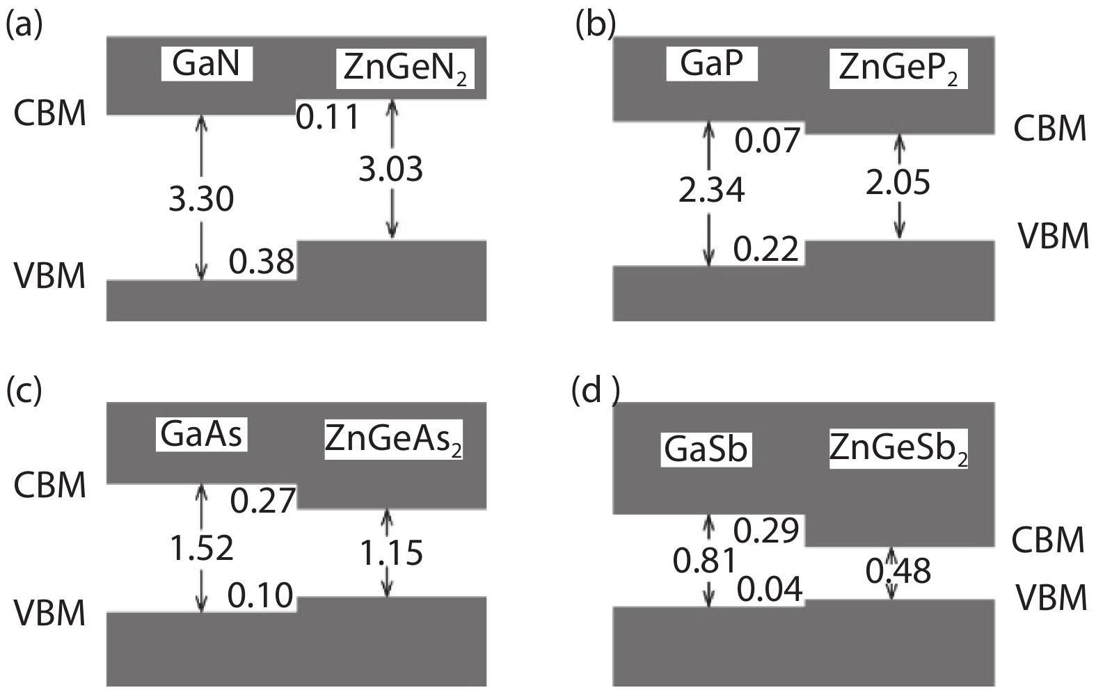
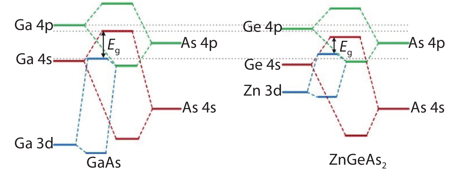
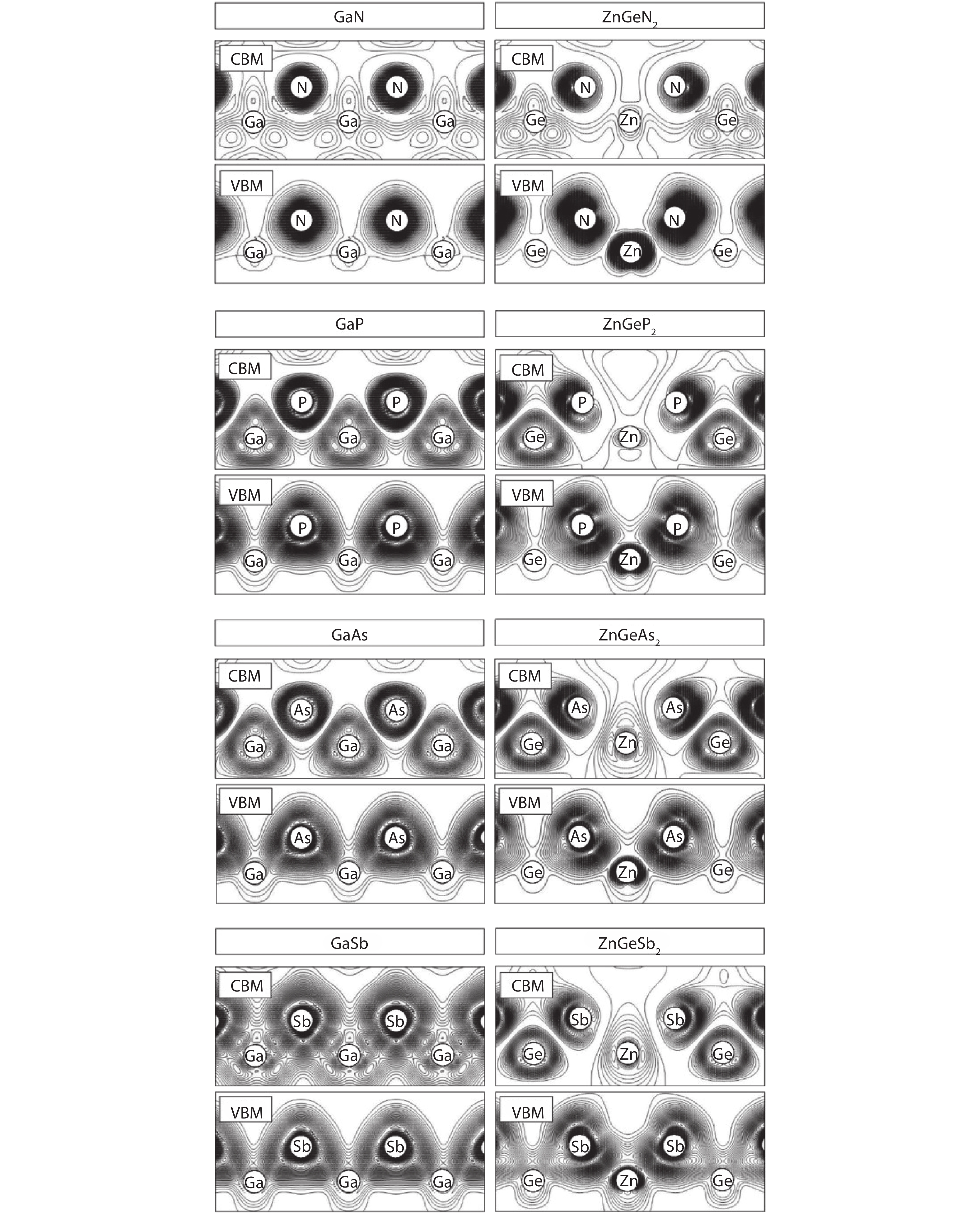
Table 1. Calculated lattice constants, bond lengths and band gaps of GaX and ZnGeX2 (X = N, P, As, Sb) compounds using HSE functional compared with experimental values.
| Crystal | Lattice constant (Å) HSE (Exp.) | Bond length (Å) HSE (Exp.) | Band gap (eV) HSE (Exp.) |
| GaN | a = b = c = 4.512 (4.50) | 1.954 (1.949) | 3.12 (3.30[20]) |
| GaP | a = b = c = 5.483 (5.45) | 2.374 (2.360) | 2.32 (2.34[21]) |
| GaAs | a = b = c = 5.695 (5.65) | 2.466 (2.448) | 1.35 (1.52[20]) |
| GaSb | a = b = c = 6.154 (6.10) | 2.665 (2.640) | 0.79 (0.81[20]) |
| ZnGeN2 | a = b = 4.572, c = 8.776 | (Ge–N) 1.871, (Zn–N) 2.043 | 3.03 |
| ZnGeP2 | a = b = 5.473 (5.46), c = 10.749 (10.76) | (Ge–P) 2.334 (2.309), (Zn–P) 2.378 (2.398) | 2.02 (2.05[22]) |
| ZnGeAs2 | a = b = 5.711 (5.67), c = 11.226 (11.15) | (Ge–As) 2.446 (2.396), (Zn–As) 2.472 (2.488) | 1.07 (1.15[23]) |
| ZnGeSb2 | a = b = 6.156, c = 12.193 | (Ge–Sb) 2.664, (Zn–Sb) 2.650 | 0.48 |
 DownLoad: CSV
Table 2. Atomic energy levels (eV) of valence states of elements studied in this paper.
| Orbit | N | P | As | Sb | Zn | Ga | Ge |
| n s | −18.49 | −14.09 | −14.77 | −13.16 | −6.31 | −9.25 | −12.03 |
| n p | −7.32 | −5.68 | −5.42 | −5.08 | −1.31 | −2.82 | −4.13 |
| (n − 1) d | − | − | −40.60 | −33.32 | −10.49 | −19.18 | −29.57 |
DownLoad: CSV
| [1] |
Yoon J, Jo S, Chun I S, et al. GaAs photovoltaics and optoelectronics using releasable multilayer epitaxial assemblies. Nature, 2010, 465, 329 doi: 10.1038/nature09054
|
| [2] |
Kent P R C, Hart Gus L W, Zunger A. Biaxial strain-modified valence and conduction band offsets of zinc-blende GaN, GaP, GaAs, InN, InP, and InAs, and optical bowing of strained epitaxial InGaN alloys. Appl Phys Lett, 2002, 81, 4377 doi: 10.1063/1.1524299
|
| [3] |
Monroy E, Munoz E, Sanchez F J, et al. High-performance GaN p–n junction photodetectors for solar ultraviolet applications. Semicond Sci Technol, 1998, 13, 1042 doi: 10.1088/0268-1242/13/9/013
|
| [4] |
Paudel T R, Lambrecht W R L. First-principles calculations of elasticity, polarization-related properties, and nonlinear optical coefficients in Zn–IV–N2 compounds. Phys Rev B, 2009, 79, 245205 doi: 10.1103/PhysRevB.79.245205
|
| [5] |
Punya A, Lambrecht W R L, Schilfgaarde M. Quasiparticle band structure of Zn–IV–N2 compounds. Phys Rev B, 2011, 84, 165204 doi: 10.1103/PhysRevB.84.165204
|
| [6] |
Ma J, Deng H X, Luo J W, et al. Origin of the failed ensemble average rule for the band gaps of disordered nonisovalent semiconductor alloys. Phys Rev B, 2014, 90, 115201 doi: 10.1103/PhysRevB.90.115201
|
| [7] |
Du K, Bekele C, Hayman C C, et al. Synthesis and characterization of ZnGeN2 grown from elemental Zn and Ge sources. J Cryst Growth, 2008, 310, 1057 doi: 10.1016/j.jcrysgro.2007.12.042
|
| [8] |
Clément Q, Melkonian J, Barrientos-Barria J, et al. Tunable optical parametric amplification of a single-frequency quantum cascade laser around 8μm in ZnGeP2. Opt Lett, 2013, 38, 4046 doi: 10.1364/OL.38.004046
|
| [9] |
Narang P, Chen S, Coronel N C, et al. Bandgap tunability in Zn(Sn, Ge)N2 semiconductor alloys. Adv Mater, 2014, 26, 1235 doi: 10.1002/adma.v26.8
|
| [10] |
Zhang S R, Xie L H, Ouyang S D, et al. Electronic structure, chemical bonding and optical properties of the nonlinear optical crystal ZnGeP2 by first-principles calculations. Phys Scri, 2016, 91, 015801 doi: 10.1088/0031-8949/91/1/015801
|
| [11] |
Kowalczyk S P, Cheung J T, Kraut E A, et al. CdTe-HgTe (-1, -1, -1) heterojunction valence-band discontinuity: A common-anion-rule contradiction. Phys Rev Lett, 1986, 56, 1605 doi: 10.1103/PhysRevLett.56.1605
|
| [12] |
Deng H X, Luo J W, Wei S H. Chemical trends of stability and band alignment of lattice-matched II–VI/III–V semiconductor interfaces. Phys Rev B, 2015, 91, 075315 doi: 10.1103/PhysRevB.91.075315
|
| [13] |
Hohenberg P, Kohn W. Inhomogeneous electron gas. Phys Rev, 1964, 136, 864 doi: 10.1103/PhysRev.136.B864
|
| [14] |
Kohn W, Sham L J. Self-consistent equations including exchange and correlation effects. Phys Rev, 1965, 140, 1133 doi: 10.1103/PhysRev.140.A1133
|
| [15] |
Heyd J, Scuseria G E, Ernzerhof M. Hybrid functionals based on a screened Coulomb potential. J Chem Phys, 2003, 118, 8207 doi: 10.1063/1.1564060
|
| [16] |
Kresse G, Furthmuller J. Efficiency of ab-initio total energy calculations for metals and semiconductors using a plane-wave basis set. Compute Mater Sci, 1996, 6, 15 doi: 10.1016/0927-0256(96)00008-0
|
| [17] |
Kresse G, Furthmüller J. Efficient iterative schemes for ab initio total-energy calculations using a plane-wave basis set. Phys Rev B, 1996, 54, 11169 doi: 10.1103/PhysRevB.54.11169
|
| [18] |
Wadehra A, Nicklas J W, Wilkins J W. Band offsets of semiconductor heterostructures: A hybrid density functional study. Appl Phys Lett, 2010, 97, 092119 doi: 10.1063/1.3487776
|
| [19] |
Blöchl P E. Projector augmented wave method. Phys Rev B, 1994, 50, 17953 doi: 10.1103/PhysRevB.50.17953
|
| [20] |
Vurgaftman I, Meyer J, Ram-Mohan L. Band parameters for III–V compound semiconductors and their alloys. J Appl Phys, 2001, 89, 5815 doi: 10.1063/1.1368156
|
| [21] |
Lorenz M R, Pettit G D, Taylor R C. Band gap of gallium phosphide from 0 to 900 °K and light emission from diodes at high temperatures. Phys Rev, 1986, 171, 876 doi: 10.1103/PhysRev.171.876
|
| [22] |
Ullah S, Murtaza G, Khenata R, et al. Towards from indirect to direct band gap and optical properties of XYP2 (X = Zn, Cd; Y = Si, Ge, Sn). Physica B, 2014, 441, 94 doi: 10.1016/j.physb.2014.02.021
|
| [23] |
Solomon G S, Timmons M L, Posthill J B. Organometallic vapor-phase-epitaxial growth and characterization of ZnGeAs2 on GaAs. J Appl Phys, 1989, 65, 1952 doi: 10.1063/1.342884
|
| [24] |
Wei S H, Zunger A. Calculated natural band offsets of all II–VI and III–V semiconductors: Chemical trends and the role of cation d orbitals. Appl Phys Lett, 1998, 72, 2011 doi: 10.1063/1.121249
|
| [25] |
Wei S H, Zunger A. Role of d orbitals in valence-band offsets of common-anion semiconductors. Phys Rev Lett, 1987, 59, 144 doi: 10.1103/PhysRevLett.59.144
|
| [26] |
Wei S H, Zunger A. Role of metal d states in II–VI semiconductors. Phys Rev B, 1988, 37, 8958 doi: 10.1103/PhysRevB.37.8958
|


Article views: 4758 Times PDF downloads: 77 Times Cited by: 0 Times
Received: 17 February 2019 Revised: Online: Accepted Manuscript: 27 February 2019Uncorrected proof: 27 February 2019Published: 08 April 2019
| Citation: |
Ruyue Cao, Hui-Xiong Deng, Jun-Wei Luo, Su-Huai Wei. Origin of the anomalous trends in band alignment of GaX/ZnGeX2 (X = N, P, As, Sb) heterojunctions[J]. Journal of Semiconductors, 2019, 40(4): 042102. doi: 10.1088/1674-4926/40/4/042102
****
R Y Cao, H X Deng, J W Luo, S H Wei, Origin of the anomalous trends in band alignment of GaX/ZnGeX2 (X = N, P, As, Sb) heterojunctions[J]. J. Semicond., 2019, 40(4): 042102. doi: 10.1088/1674-4926/40/4/042102.

|
| [1] |
Yoon J, Jo S, Chun I S, et al. GaAs photovoltaics and optoelectronics using releasable multilayer epitaxial assemblies. Nature, 2010, 465, 329 doi: 10.1038/nature09054
|
| [2] |
Kent P R C, Hart Gus L W, Zunger A. Biaxial strain-modified valence and conduction band offsets of zinc-blende GaN, GaP, GaAs, InN, InP, and InAs, and optical bowing of strained epitaxial InGaN alloys. Appl Phys Lett, 2002, 81, 4377 doi: 10.1063/1.1524299
|
| [3] |
Monroy E, Munoz E, Sanchez F J, et al. High-performance GaN p–n junction photodetectors for solar ultraviolet applications. Semicond Sci Technol, 1998, 13, 1042 doi: 10.1088/0268-1242/13/9/013
|
| [4] |
Paudel T R, Lambrecht W R L. First-principles calculations of elasticity, polarization-related properties, and nonlinear optical coefficients in Zn–IV–N2 compounds. Phys Rev B, 2009, 79, 245205 doi: 10.1103/PhysRevB.79.245205
|
| [5] |
Punya A, Lambrecht W R L, Schilfgaarde M. Quasiparticle band structure of Zn–IV–N2 compounds. Phys Rev B, 2011, 84, 165204 doi: 10.1103/PhysRevB.84.165204
|
| [6] |
Ma J, Deng H X, Luo J W, et al. Origin of the failed ensemble average rule for the band gaps of disordered nonisovalent semiconductor alloys. Phys Rev B, 2014, 90, 115201 doi: 10.1103/PhysRevB.90.115201
|
| [7] |
Du K, Bekele C, Hayman C C, et al. Synthesis and characterization of ZnGeN2 grown from elemental Zn and Ge sources. J Cryst Growth, 2008, 310, 1057 doi: 10.1016/j.jcrysgro.2007.12.042
|
| [8] |
Clément Q, Melkonian J, Barrientos-Barria J, et al. Tunable optical parametric amplification of a single-frequency quantum cascade laser around 8μm in ZnGeP2. Opt Lett, 2013, 38, 4046 doi: 10.1364/OL.38.004046
|
| [9] |
Narang P, Chen S, Coronel N C, et al. Bandgap tunability in Zn(Sn, Ge)N2 semiconductor alloys. Adv Mater, 2014, 26, 1235 doi: 10.1002/adma.v26.8
|
| [10] |
Zhang S R, Xie L H, Ouyang S D, et al. Electronic structure, chemical bonding and optical properties of the nonlinear optical crystal ZnGeP2 by first-principles calculations. Phys Scri, 2016, 91, 015801 doi: 10.1088/0031-8949/91/1/015801
|
| [11] |
Kowalczyk S P, Cheung J T, Kraut E A, et al. CdTe-HgTe (-1, -1, -1) heterojunction valence-band discontinuity: A common-anion-rule contradiction. Phys Rev Lett, 1986, 56, 1605 doi: 10.1103/PhysRevLett.56.1605
|
| [12] |
Deng H X, Luo J W, Wei S H. Chemical trends of stability and band alignment of lattice-matched II–VI/III–V semiconductor interfaces. Phys Rev B, 2015, 91, 075315 doi: 10.1103/PhysRevB.91.075315
|
| [13] |
Hohenberg P, Kohn W. Inhomogeneous electron gas. Phys Rev, 1964, 136, 864 doi: 10.1103/PhysRev.136.B864
|
| [14] |
Kohn W, Sham L J. Self-consistent equations including exchange and correlation effects. Phys Rev, 1965, 140, 1133 doi: 10.1103/PhysRev.140.A1133
|
| [15] |
Heyd J, Scuseria G E, Ernzerhof M. Hybrid functionals based on a screened Coulomb potential. J Chem Phys, 2003, 118, 8207 doi: 10.1063/1.1564060
|
| [16] |
Kresse G, Furthmuller J. Efficiency of ab-initio total energy calculations for metals and semiconductors using a plane-wave basis set. Compute Mater Sci, 1996, 6, 15 doi: 10.1016/0927-0256(96)00008-0
|
| [17] |
Kresse G, Furthmüller J. Efficient iterative schemes for ab initio total-energy calculations using a plane-wave basis set. Phys Rev B, 1996, 54, 11169 doi: 10.1103/PhysRevB.54.11169
|
| [18] |
Wadehra A, Nicklas J W, Wilkins J W. Band offsets of semiconductor heterostructures: A hybrid density functional study. Appl Phys Lett, 2010, 97, 092119 doi: 10.1063/1.3487776
|
| [19] |
Blöchl P E. Projector augmented wave method. Phys Rev B, 1994, 50, 17953 doi: 10.1103/PhysRevB.50.17953
|
| [20] |
Vurgaftman I, Meyer J, Ram-Mohan L. Band parameters for III–V compound semiconductors and their alloys. J Appl Phys, 2001, 89, 5815 doi: 10.1063/1.1368156
|
| [21] |
Lorenz M R, Pettit G D, Taylor R C. Band gap of gallium phosphide from 0 to 900 °K and light emission from diodes at high temperatures. Phys Rev, 1986, 171, 876 doi: 10.1103/PhysRev.171.876
|
| [22] |
Ullah S, Murtaza G, Khenata R, et al. Towards from indirect to direct band gap and optical properties of XYP2 (X = Zn, Cd; Y = Si, Ge, Sn). Physica B, 2014, 441, 94 doi: 10.1016/j.physb.2014.02.021
|
| [23] |
Solomon G S, Timmons M L, Posthill J B. Organometallic vapor-phase-epitaxial growth and characterization of ZnGeAs2 on GaAs. J Appl Phys, 1989, 65, 1952 doi: 10.1063/1.342884
|
| [24] |
Wei S H, Zunger A. Calculated natural band offsets of all II–VI and III–V semiconductors: Chemical trends and the role of cation d orbitals. Appl Phys Lett, 1998, 72, 2011 doi: 10.1063/1.121249
|
| [25] |
Wei S H, Zunger A. Role of d orbitals in valence-band offsets of common-anion semiconductors. Phys Rev Lett, 1987, 59, 144 doi: 10.1103/PhysRevLett.59.144
|
| [26] |
Wei S H, Zunger A. Role of metal d states in II–VI semiconductors. Phys Rev B, 1988, 37, 8958 doi: 10.1103/PhysRevB.37.8958
|

 WeChat ID
Journal of Semiconductors © 2017 All Rights Reserved 京ICP备05085259号-2


