


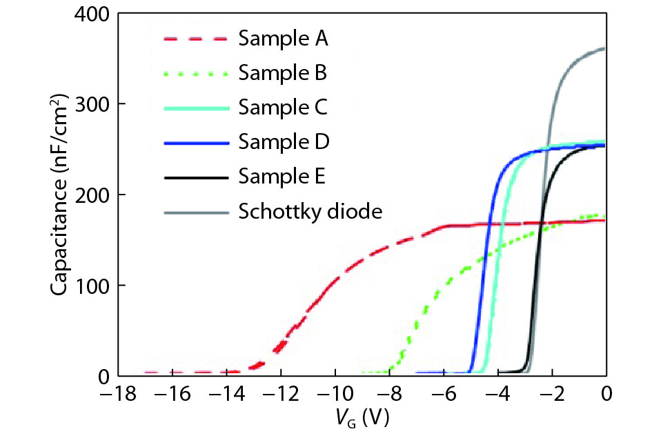
Fig. 1.
(Color online) C–V characteristics at 1 MHz for all the diodes.
ARTICLES
Shuxin Tan1, and Takashi Egawa2
Corresponding author: Shuxin Tan, email: tansx2014@ntu.edu.cn
Abstract: AlGaN/GaN metal–insulator–semiconductor high-electron-mobility transistors (MIS-HEMTs) on a silicon substrate were fabricated with silicon oxide as a gate dielectric by sputtering deposition and electron-beam (EB) evaporation. It was found that the oxide deposition method and conditions have great influences on the electrical properties of HEMTs. The low sputtering temperature or oxygen introduction at higher temperature results in a positive equivalent charge density at the oxide/AlGaN interface (Nequ), which induces a negative shift of threshold voltage and an increase in both sheet electron density (ns) and drain current density (ID). Contrarily, EB deposition makes a negative Nequ, resulting in reduced ns and ID. Besides, the maximum transconductance (gm-max) decreases and the off-state gate current density (IG-off) increases for oxides at lower sputtering temperature compared with that at higher temperature, possibly due to a more serious sputter-induced damage and much larger Nequ at lower sputtering temperature. At high sputtering temperature, IG-off decreases by two orders of magnitude compared to that without oxygen, which indicates that oxygen introduction and partial pressure depression of argon decreases the sputter-induced damage significantly. IG-off for EB-evaporated samples is lower by orders of magnitude than that of sputtered ones, possibly attributed to the lower damage of EB evaporation to the barrier layer surface.
Keywords: AlGaN/GaN MIS-HEMTs, sputtering deposition, electron-beam evaporation, silicon oxide, electrical properties
| [1] |
Acharyya A. Hot electron transport in wurtzite-GaN: effects of temperature and doping concentration. J Semicond, 2018, 39(7), 072002 doi: 10.1088/1674-4926/39/7/072002
|
| [2] |
Liang F, Zhao D G, Jiang D S, et al. Performance enhancement of the GaN-based laser diode by using an unintentionally doped GaN upper waveguide. Jpn J Appl Phys, 2018, 57, 070307 doi: 10.7567/JJAP.57.070307
|
| [3] |
Huang X, Du C, Zhou Y, et al. Piezo-phototronic effect in a quantum well structure. ACS Nano, 2016, 10, 5145 doi: 10.1021/acsnano.6b00417
|
| [4] |
Li X, Ma P, Ji X, et al. Implementation of slow and smooth etching of GaN by inductively coupled plasma. J Semicond, 2018, 39(11), 113002 doi: 10.1088/1674-4926/39/11/113002
|
| [5] |
Tzou A, Chu K H, Lin I F, et al. AlN surface passivation of GaN-based high electron mobility transistors by plasma-enhanced atomic layer deposition. Nanoscale Res Lett, 2017, 12, 315 doi: 10.1186/s11671-017-2082-0
|
| [6] |
Li D, Sun X, Song H, et al. Realization of a high-performance GaN UV detector by nanoplasmonic enhancement. Adv Mater, 2012, 24, 845 doi: 10.1002/adma.201102585
|
| [7] |
Zhao D G, Zhu J J, Liu Z S, et al. Surface morphology of AlN buffer layer and its effect on the GaN growth by metalorganic vapor chemical deposition. Appl Phys Lett, 2004, 85, 1499 doi: 10.1063/1.1784034
|
| [8] |
Tan S, Deng X, Zhang B, et al. Thermal stability of F ion-implant isolated AlGaN/GaN heterostructures. Sci China-Phys Mech Astron, 2018, 61, 127311 doi: 10.1007/s11433-018-9312-7
|
| [9] |
Zhao S X, Liu X Y, Zhang L Q, et al. Impacts of thermal atomic layer-deposited AlN passivation layer on GaN-on-Si high electron mobility transistors. Nanoscale Res Lett, 2016, 11, 137 doi: 10.1186/s11671-016-1335-7
|
| [10] |
Meneghesso G, Meneghini M, Bisi D, et al. Trapping and reliability issues in GaN-based MIS HEMTs with partially recessed gate. Microelectron Reliab, 2016, 58, 151 doi: 10.1016/j.microrel.2015.11.024
|
| [11] |
Lagger P, Steinschifter P, Reiner M, et al. Role of the dielectric for the charging dynamics of the dielectric/barrier interface in AlGaN/GaN based metal-insulator semiconductor structures under forward gate bias stress. Appl Phys Lett, 2014, 105, 033512 doi: 10.1063/1.4891532
|
| [12] |
Sugiura S, Kishimoto S, Mizutani T, et al. Normally-off AlGaN/GaN MOSFETs with HfO2 gate oxide. Phys Stat Sol C, 2008, 5, 1923 doi: 10.1002/pssc.200778449
|
| [13] |
Hashizume T, Anantathanasarn S, Negoro N, et al. Al2O3 insulated-gate structure for AlGaN/GaN heterostructure field effect transistors having thin AlGaN barrier layers. Jpn J Appl Phys, 2004, 43, L777 doi: 10.1143/JJAP.43.L777
|
| [14] |
Van Hove M, Kang X, Stoffels S, et al. Fabrication and performance of Au-free AlGaN/GaN-on-silicon power devices with Al2O3 and Si3N4/Al2O3 gate dielectrics. IEEE Trans Electron Devices, 2013, 60, 3071 doi: 10.1109/TED.2013.2274730
|
| [15] |
Liu T, Jiang C, Huang X, et al. Electrical transportation and piezotronic-effect modulation in AlGaN/GaN MOS HEMTs and unpassivated HEMTs. Nano Energy, 2017, 39, 53 doi: 10.1016/j.nanoen.2017.06.041
|
| [16] |
Shih H Y, Chu F C, Lee C Y, et al. Atomic layer deposition of gallium oxide films as gate dielectrics in AlGaN/GaN metal–oxide–semiconductor high-electron-mobility transistors. Nanoscale Res Lett, 2016, 11, 235 doi: 10.1186/s11671-016-1448-z
|
| [17] |
Derluyn J, Boeykens S, Cheng K, et al. Improvement of AlGaN GaN high electron mobility transistor structures by in situ deposition of a Si3N4 surface layer. J Appl Phys, 2005, 98, 054501 doi: 10.1063/1.2008388
|
| [18] |
Ao J P, Nakatani K, Ohmuro K, et al. GaN metal–oxide–semiconductor field-effect transistor with tetraethylorthosilicate SiO2 gate insulator on AlGaN/GaN heterostructure. Jpn J Appl Phys, 2010, 49, 04DF09 doi: 10.1143/JJAP.48.04C095
|
| [19] |
Asif Khan M, Hu X, Tarakji A, et al. AlGaN/GaN metal–oxide–semiconductor heterostructure field-effect transistors on SiC substrates. Appl Phys Lett, 2000, 77, 1339 doi: 10.1063/1.1290269
|
| [20] |
Liu C, Chor E F, Tan L S. Investigations of HfO2/AlGaN/GaN metal–oxide–semiconductor high electron mobility transistors. Appl Phys Lett, 2006, 88, 173504 doi: 10.1063/1.2198507
|
| [21] |
Tan S, Selvaraj S L, Egawa T. Metal–organic chemical vapor deposition of quasi-normally-off AlGaN/GaN filed-effect transistors on silicon substrates using low-temperature gown AlN cap layers. Appl Phys Lett, 2010, 97, 053502 doi: 10.1063/1.3475394
|
| [22] |
Ronchi N, De Jaeger B, Van Hove M, et al. Combined plasma-enhanced-atomic-layer-deposition gate dielectric and in situ SiN cap layer for reduced threshold voltage shift and dynamic ON-resistance dispersion of AlGaN/GaN high electron mobility transistors on 200 mm Si substrates. Jpn J Appl Phys, 2015, 54, 04DF02 doi: 10.7567/JJAP.54.04DF02
|
| [23] |
Lee J G, Kim H S, Seo K S, et al. High quality PECVD SiO2 process for recessed MOS-gate of AlGaN/GaN-on-Si metal–oxide–semiconductor heterostructure field-effect transistors. Solid State Electron, 2015, 122, 32 doi: 10.1016/j.sse.2016.04.016
|
| [24] |
Fiorenza P, Greco G, Iucolano F, et al. Slow and fast traps in metal–oxide–semiconductor capacitors fabricated on recessed AlGaN/GaN heterostructures. Appl Phys Lett, 2015, 106, 142903 doi: 10.1063/1.4917250
|
| [25] |
Sun X, Li D, Jiang H, et al. Improved performance of GaN metal–semiconductor–metal ultraviolet detectors by depositing SiO2 nanoparticles on a GaN surface. Appl Phys Lett, 2011, 98, 121117 doi: 10.1063/1.3567943
|
| [26] |
Dutta G, Das Gupta N, Das Gupta A. Effect of sputtered-Al2O3 layer thickness on the threshold voltage of III-nitride MIS-HEMTs. IEEE Trans Electron Devices, 2016, 63, 1450 doi: 10.1109/TED.2016.2529428
|
| [27] |
Tuan T, Kuo D H. Characteristics of RF reactive sputter-deposited Pt/SiO2/n-InGaN MOS Schottky diodes. Mater Sci Semicon Proc, 2015, 30, 314 doi: 10.1016/j.mssp.2014.10.021
|
| [28] |
Xirouchaki C, Palmer R E. Deposition of size-selected metal clusters generated by magnetron sputtering and gas condensation: a progress review. Phil Trans R Soc Lond A, 2004, 362, 117 doi: 10.1098/rsta.2003.1306
|
| [29] |
Maeda N, Hiroki M, Watanabe N, et al. Systematic study of insulator deposition effect (Si3N4, SiO2, AlN, and Al2O3) on electrical properties in AlGaN/GaN heterostructures. Jpn J Appl Phys, 2007, 46, 547 doi: 10.1143/JJAP.46.547
|
| [30] |
Ambacher O, Majewski J, Miskys C, et al. Pyroelectric properties of Al(In)GaN/GaN hetero- and quantum well structures. J Phys: Condens Matter, 2002, 14, 3399 doi: 10.1088/0953-8984/14/13/302
|
| [31] |
Zhu J J, Ma X H, Xie Y, et al. Improved interface and transport properties of AlGaN/GaN MIS-HEMTs with PEALD-grown AlN gate dielectric. IEEE Trans Electron Devices, 2015, 62, 512 doi: 10.1109/TED.2014.2377781
|
| [32] |
Seok O, Ahn W, Han M K, et al. Effect of Ga2O3 sputtering power on breakdown voltage of AlGaN/GaN high-electron-mobility transistors. J Vac Sci Tech B, 2013, 31, 011203 doi: 10.1116/1.4769863
|
| [33] |
Chang S J, Lan C H, Hwang J D, et al. Sputtered indium-tin-oxide on p-GaN. J Electrochem Soc, 2008, 155, H140 doi: 10.1149/1.2820626
|
| [34] |
Stoklas R, Gregušová D, Gaži Š, et al. Performance of AlGaN/GaN metal–insulator–semiconductor heterostructure field-effect transistors with AlN gate insulator prepared by reactive magnetron sputtering. J Vac Sci Tech B, 2011, 29, 01A809 doi: 10.1116/1.3523362
|


Article views: 3991 Times PDF downloads: 75 Times Cited by: 0 Times
Received: 28 December 2018 Revised: 08 January 2019 Online: Accepted Manuscript: 19 February 2019Uncorrected proof: 22 February 2019Published: 08 April 2019
| Citation: |
Shuxin Tan, Takashi Egawa. Influence of growth conditions of oxide on electrical properties of AlGaN/GaN metal–insulator–semiconductor transistors[J]. Journal of Semiconductors, 2019, 40(4): 042801. doi: 10.1088/1674-4926/40/4/042801
****
S X Tan, T Egawa, Influence of growth conditions of oxide on electrical properties of AlGaN/GaN metal–insulator–semiconductor transistors[J]. J. Semicond., 2019, 40(4): 042801. doi: 10.1088/1674-4926/40/4/042801.

|
| [1] |
Acharyya A. Hot electron transport in wurtzite-GaN: effects of temperature and doping concentration. J Semicond, 2018, 39(7), 072002 doi: 10.1088/1674-4926/39/7/072002
|
| [2] |
Liang F, Zhao D G, Jiang D S, et al. Performance enhancement of the GaN-based laser diode by using an unintentionally doped GaN upper waveguide. Jpn J Appl Phys, 2018, 57, 070307 doi: 10.7567/JJAP.57.070307
|
| [3] |
Huang X, Du C, Zhou Y, et al. Piezo-phototronic effect in a quantum well structure. ACS Nano, 2016, 10, 5145 doi: 10.1021/acsnano.6b00417
|
| [4] |
Li X, Ma P, Ji X, et al. Implementation of slow and smooth etching of GaN by inductively coupled plasma. J Semicond, 2018, 39(11), 113002 doi: 10.1088/1674-4926/39/11/113002
|
| [5] |
Tzou A, Chu K H, Lin I F, et al. AlN surface passivation of GaN-based high electron mobility transistors by plasma-enhanced atomic layer deposition. Nanoscale Res Lett, 2017, 12, 315 doi: 10.1186/s11671-017-2082-0
|
| [6] |
Li D, Sun X, Song H, et al. Realization of a high-performance GaN UV detector by nanoplasmonic enhancement. Adv Mater, 2012, 24, 845 doi: 10.1002/adma.201102585
|
| [7] |
Zhao D G, Zhu J J, Liu Z S, et al. Surface morphology of AlN buffer layer and its effect on the GaN growth by metalorganic vapor chemical deposition. Appl Phys Lett, 2004, 85, 1499 doi: 10.1063/1.1784034
|
| [8] |
Tan S, Deng X, Zhang B, et al. Thermal stability of F ion-implant isolated AlGaN/GaN heterostructures. Sci China-Phys Mech Astron, 2018, 61, 127311 doi: 10.1007/s11433-018-9312-7
|
| [9] |
Zhao S X, Liu X Y, Zhang L Q, et al. Impacts of thermal atomic layer-deposited AlN passivation layer on GaN-on-Si high electron mobility transistors. Nanoscale Res Lett, 2016, 11, 137 doi: 10.1186/s11671-016-1335-7
|
| [10] |
Meneghesso G, Meneghini M, Bisi D, et al. Trapping and reliability issues in GaN-based MIS HEMTs with partially recessed gate. Microelectron Reliab, 2016, 58, 151 doi: 10.1016/j.microrel.2015.11.024
|
| [11] |
Lagger P, Steinschifter P, Reiner M, et al. Role of the dielectric for the charging dynamics of the dielectric/barrier interface in AlGaN/GaN based metal-insulator semiconductor structures under forward gate bias stress. Appl Phys Lett, 2014, 105, 033512 doi: 10.1063/1.4891532
|
| [12] |
Sugiura S, Kishimoto S, Mizutani T, et al. Normally-off AlGaN/GaN MOSFETs with HfO2 gate oxide. Phys Stat Sol C, 2008, 5, 1923 doi: 10.1002/pssc.200778449
|
| [13] |
Hashizume T, Anantathanasarn S, Negoro N, et al. Al2O3 insulated-gate structure for AlGaN/GaN heterostructure field effect transistors having thin AlGaN barrier layers. Jpn J Appl Phys, 2004, 43, L777 doi: 10.1143/JJAP.43.L777
|
| [14] |
Van Hove M, Kang X, Stoffels S, et al. Fabrication and performance of Au-free AlGaN/GaN-on-silicon power devices with Al2O3 and Si3N4/Al2O3 gate dielectrics. IEEE Trans Electron Devices, 2013, 60, 3071 doi: 10.1109/TED.2013.2274730
|
| [15] |
Liu T, Jiang C, Huang X, et al. Electrical transportation and piezotronic-effect modulation in AlGaN/GaN MOS HEMTs and unpassivated HEMTs. Nano Energy, 2017, 39, 53 doi: 10.1016/j.nanoen.2017.06.041
|
| [16] |
Shih H Y, Chu F C, Lee C Y, et al. Atomic layer deposition of gallium oxide films as gate dielectrics in AlGaN/GaN metal–oxide–semiconductor high-electron-mobility transistors. Nanoscale Res Lett, 2016, 11, 235 doi: 10.1186/s11671-016-1448-z
|
| [17] |
Derluyn J, Boeykens S, Cheng K, et al. Improvement of AlGaN GaN high electron mobility transistor structures by in situ deposition of a Si3N4 surface layer. J Appl Phys, 2005, 98, 054501 doi: 10.1063/1.2008388
|
| [18] |
Ao J P, Nakatani K, Ohmuro K, et al. GaN metal–oxide–semiconductor field-effect transistor with tetraethylorthosilicate SiO2 gate insulator on AlGaN/GaN heterostructure. Jpn J Appl Phys, 2010, 49, 04DF09 doi: 10.1143/JJAP.48.04C095
|
| [19] |
Asif Khan M, Hu X, Tarakji A, et al. AlGaN/GaN metal–oxide–semiconductor heterostructure field-effect transistors on SiC substrates. Appl Phys Lett, 2000, 77, 1339 doi: 10.1063/1.1290269
|
| [20] |
Liu C, Chor E F, Tan L S. Investigations of HfO2/AlGaN/GaN metal–oxide–semiconductor high electron mobility transistors. Appl Phys Lett, 2006, 88, 173504 doi: 10.1063/1.2198507
|
| [21] |
Tan S, Selvaraj S L, Egawa T. Metal–organic chemical vapor deposition of quasi-normally-off AlGaN/GaN filed-effect transistors on silicon substrates using low-temperature gown AlN cap layers. Appl Phys Lett, 2010, 97, 053502 doi: 10.1063/1.3475394
|
| [22] |
Ronchi N, De Jaeger B, Van Hove M, et al. Combined plasma-enhanced-atomic-layer-deposition gate dielectric and in situ SiN cap layer for reduced threshold voltage shift and dynamic ON-resistance dispersion of AlGaN/GaN high electron mobility transistors on 200 mm Si substrates. Jpn J Appl Phys, 2015, 54, 04DF02 doi: 10.7567/JJAP.54.04DF02
|
| [23] |
Lee J G, Kim H S, Seo K S, et al. High quality PECVD SiO2 process for recessed MOS-gate of AlGaN/GaN-on-Si metal–oxide–semiconductor heterostructure field-effect transistors. Solid State Electron, 2015, 122, 32 doi: 10.1016/j.sse.2016.04.016
|
| [24] |
Fiorenza P, Greco G, Iucolano F, et al. Slow and fast traps in metal–oxide–semiconductor capacitors fabricated on recessed AlGaN/GaN heterostructures. Appl Phys Lett, 2015, 106, 142903 doi: 10.1063/1.4917250
|
| [25] |
Sun X, Li D, Jiang H, et al. Improved performance of GaN metal–semiconductor–metal ultraviolet detectors by depositing SiO2 nanoparticles on a GaN surface. Appl Phys Lett, 2011, 98, 121117 doi: 10.1063/1.3567943
|
| [26] |
Dutta G, Das Gupta N, Das Gupta A. Effect of sputtered-Al2O3 layer thickness on the threshold voltage of III-nitride MIS-HEMTs. IEEE Trans Electron Devices, 2016, 63, 1450 doi: 10.1109/TED.2016.2529428
|
| [27] |
Tuan T, Kuo D H. Characteristics of RF reactive sputter-deposited Pt/SiO2/n-InGaN MOS Schottky diodes. Mater Sci Semicon Proc, 2015, 30, 314 doi: 10.1016/j.mssp.2014.10.021
|
| [28] |
Xirouchaki C, Palmer R E. Deposition of size-selected metal clusters generated by magnetron sputtering and gas condensation: a progress review. Phil Trans R Soc Lond A, 2004, 362, 117 doi: 10.1098/rsta.2003.1306
|
| [29] |
Maeda N, Hiroki M, Watanabe N, et al. Systematic study of insulator deposition effect (Si3N4, SiO2, AlN, and Al2O3) on electrical properties in AlGaN/GaN heterostructures. Jpn J Appl Phys, 2007, 46, 547 doi: 10.1143/JJAP.46.547
|
| [30] |
Ambacher O, Majewski J, Miskys C, et al. Pyroelectric properties of Al(In)GaN/GaN hetero- and quantum well structures. J Phys: Condens Matter, 2002, 14, 3399 doi: 10.1088/0953-8984/14/13/302
|
| [31] |
Zhu J J, Ma X H, Xie Y, et al. Improved interface and transport properties of AlGaN/GaN MIS-HEMTs with PEALD-grown AlN gate dielectric. IEEE Trans Electron Devices, 2015, 62, 512 doi: 10.1109/TED.2014.2377781
|
| [32] |
Seok O, Ahn W, Han M K, et al. Effect of Ga2O3 sputtering power on breakdown voltage of AlGaN/GaN high-electron-mobility transistors. J Vac Sci Tech B, 2013, 31, 011203 doi: 10.1116/1.4769863
|
| [33] |
Chang S J, Lan C H, Hwang J D, et al. Sputtered indium-tin-oxide on p-GaN. J Electrochem Soc, 2008, 155, H140 doi: 10.1149/1.2820626
|
| [34] |
Stoklas R, Gregušová D, Gaži Š, et al. Performance of AlGaN/GaN metal–insulator–semiconductor heterostructure field-effect transistors with AlN gate insulator prepared by reactive magnetron sputtering. J Vac Sci Tech B, 2011, 29, 01A809 doi: 10.1116/1.3523362
|

 WeChat ID
Journal of Semiconductors © 2017 All Rights Reserved 京ICP备05085259号-2

 DownLoad:

