


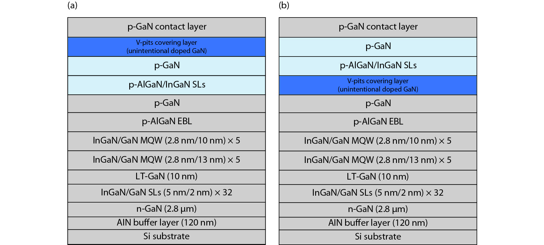
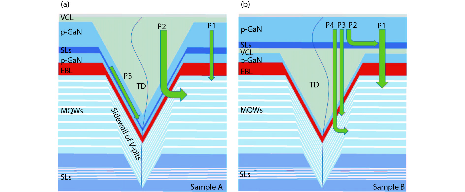
Fig. 1.
(Color online) Schematic epitaxial structures of two samples with different position of V-pits covering layer.
ARTICLES
Chen Xu, Changda Zheng, Xiaoming Wu, Shuan Pan, Xingan Jiang, Junlin Liu and Fengyi Jiang
Corresponding author: Changda Zheng, Email: zhengchangda@ncu.edu.cn
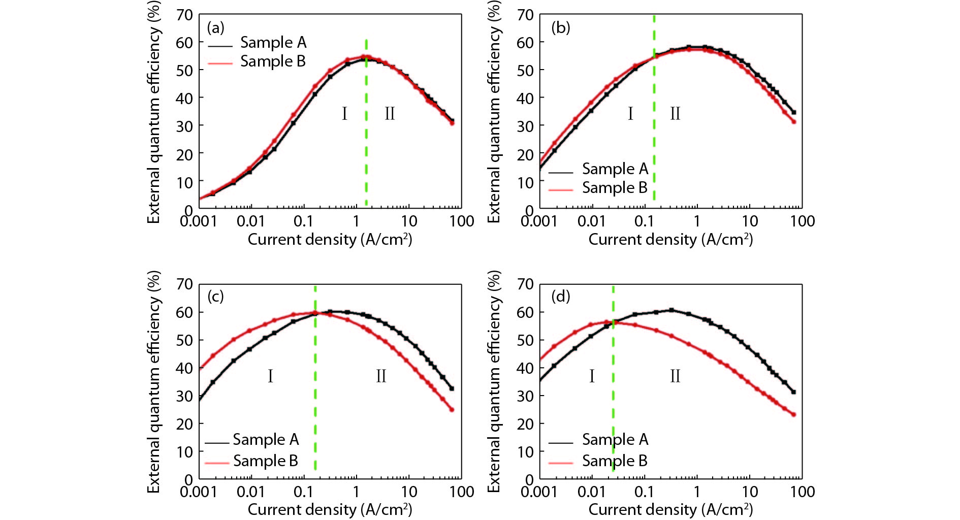
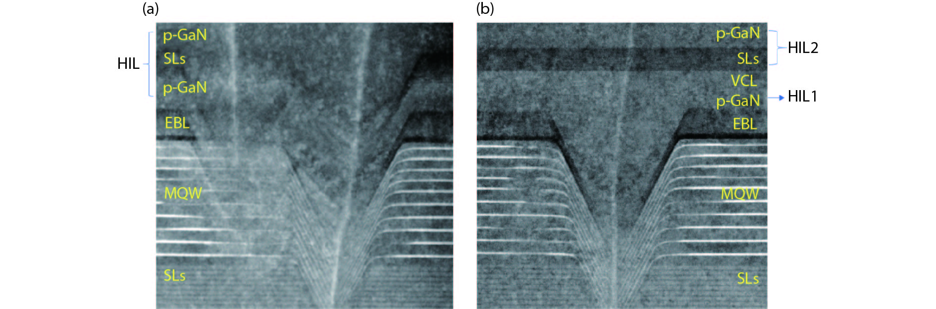
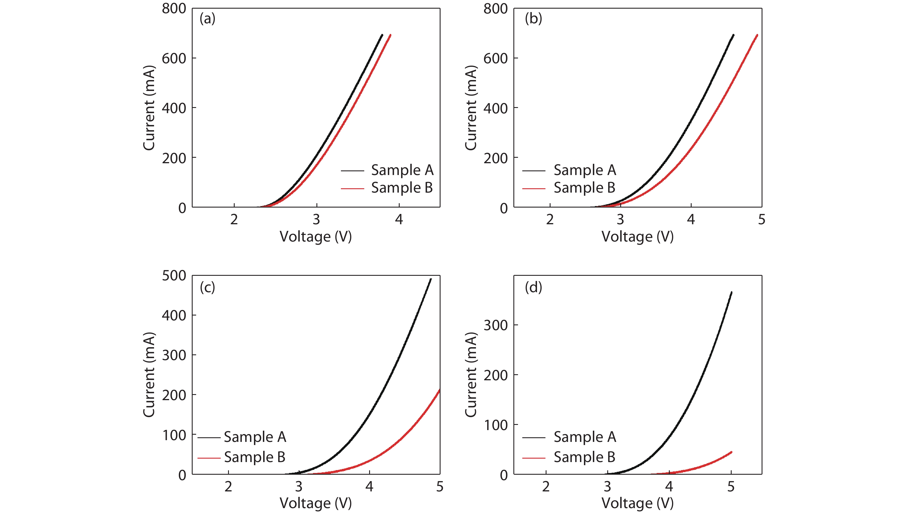
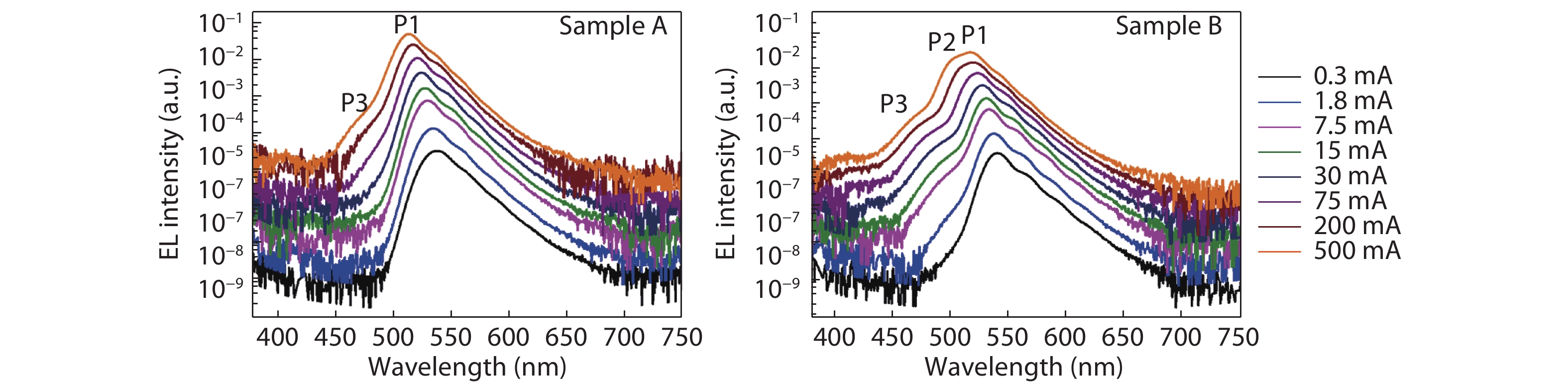
Abstract: The impact of the V-pits covering layer (VCL) position on the optoelectronic performance of InGaN-based green light-emitting diodes (LEDs) was investigated. It is found that earlier covering of V-pits will hinder the hole injection via the sidewall of V-pits, and then result in less quantum wells (QWs) participating in radioluminescence. The current-voltage characteristics show that the LEDs with earlier covering of V-pits have higher operating voltage at room temperature, and a more dramatic voltage rise with the reduction of temperature. Meanwhile, more manifested emission peaks for sidewall QWs and deeper QWs near to n-type layer was observed in the sample with earlier coveing of V-pits at cryogenic temperatures, for the reason that the holes being injected via V-pits sidewall have higher kinetic energy and could transport to deeper QWs.
Keywords: green light-emitting diodes, V-pits covering layer, hole injection efficiency, operating voltage
| [1] |
Deng G, Zhang Y, Yu Y, et al. Significantly reduced in-plane tensile stress of GaN films grown on SiC substrates by using graded AlGaN buffer and SiNx interlayer. Superlattices Microstruct, 2018, 122, 74 doi: 10.1016/j.spmi.2018.08.020
|
| [2] |
Yan L, Zhang Y, Han X, et al. Polarization-induced hole doping in N-polar III-nitride LED grown by metalorganic chemical vapor deposition. Appl Phys Lett, 2018, 112(18), 182104 doi: 10.1063/1.5023521
|
| [3] |
Deng G, Zhang Y, Yu Y, et al. Significantly improved surface morphology of N-polar GaN film grown on SiC substrate by the optimization of V/III ratio. Appl Phys Lett, 2018, 112(15), 151607 doi: 10.1063/1.5022237
|
| [4] |
Deng G, Zhang Y, Yu Y, et al. Study on the structural, optical, and electrical properties of the yellow light-emitting diode grown on free-standing (0001) GaN substrate. Superlattices Microstruct, 2018, 116, 1 doi: 10.1016/j.spmi.2018.01.033
|
| [5] |
Junlin L, Jianli Z, Guangxu W, et al. Status of GaN-based green light-emitting diodes. Chin Phys B, 2015, 24(6), 39
|
| [6] |
Crawford M H. LEDs for solid-state lighting: performance challenges and recent advances. IEEE J Sel Top Quantum Electron, 2009, 15(4), 1028 doi: 10.1109/JSTQE.2009.2013476
|
| [7] |
Piprek J. Origin of InGaN/GaN light-emitting diode efficiency improvements using tunnel-junction-cascaded active regions. Appl Phys Lett, 2014, 104(5), 2217 doi: 10.1063/1.4864311
|
| [8] |
Hangleiter A, Hitzel F, Netzel C, et al. Suppression of nonradiative recombination by V-shaped pits in GaInN/GaN quantum wells produces a large increase in the light emission efficiency. Phys Rev Lett, 2005, 95(12), 127402 doi: 10.1103/PhysRevLett.95.127402
|
| [9] |
Quan Z, Wang L, Zheng C, et al. Roles of V-shaped pits on the improvement of quantum efficiency in InGaN/GaN multiple quantum well light-emitting diodes. J Appl Phys, 2014, 116(18), A779 doi: 10.1063/1.4901828
|
| [10] |
Li Y, Yun F, Su X, et al. Deep hole injection assisted by large V-shape pits in InGaN/GaN multiple-quantum-wells blue light-emitting diodes. J Appl Phys, 2014, 116(12), 253512 doi: 10.1063/1.4896362
|
| [11] |
Zhou S, Liu X. Effect of V-pits embedded InGaN/GaN superlattices on optical and electrical properties of GaN-based green light-emitting diodes. Phys Status Solidi Appl Res, 2016, 214(5), 1770125 doi: 10.1002/pssa.201600782
|
| [12] |
Takahashi H, Ito A, Tanaka T, et al. Effect of intentionally formed `V-defects' on the emission efficiency of GaInN single. Jpn Soc Appl Phys, 2000, 39, 569 doi: 10.1143/JJAP.39.L569
|
| [13] |
Ting S M, Ramer J C, Florescu D I, et al. Morphological evolution of InGaN/GaN quantum-well heterostructures grown by metalorganic chemical vapor deposition. J Appl Phys, 2003, 94(3), 1461 doi: 10.1063/1.1586972
|
| [14] |
Le L C, Zhao D G, Jiang D S, et al. Effect of V-defects on the performance deterioration of InGaN/GaN multiple-quantum-well light-emitting diodes with varying barrier layer thickness. J Appl Phys, 2013, 114(14), 143706 doi: 10.1063/1.4824801
|
| [15] |
Lv Q, Liu J, Mo C, et al. Realization of highly efficient InGaN green LEDs with sandwich-like multiple quantum well structure: role of enhanced interwell carrier transport. ACS Photonics, 2018, 6(1), 130 doi: 10.1021/acsphotonics.8b01040
|
| [16] |
Wang G, Tao X, Liu J, et al. Temperature-dependent electroluminescence from InGaN/GaN green light-emitting diodes on silicon with different quantum-well structures. Semicond Sci Technol, 2014, 30(1), 15018 doi: 10.1088/0268-1242/30/1/015018
|
| [17] |
Wu X, Liu J, Quan Z, et al. Electroluminescence from the sidewall quantum wells in the V-shaped pits of InGaN light emitting diodes. Appl Phys Lett, 2014, 104(22), 1634 doi: 10.1063/1.4880731
|
| [18] |
Kim J, Tak Y, Kim J, et al. Analysis of forward tunneling current in InGaN/GaN multiple quantum well light-emitting diodes grown on Si (111) substrate. J Appl Phys, 2013, 114(1), 231107 doi: 10.1063/1.4812231
|
| [19] |
Kozodoy P, Xing H, Denbaars S P, et al. Heavy doping effects in Mg-doped GaN. J Appl Phys, 2000, 87(4), 1832 doi: 10.1063/1.372098
|
| [20] |
Xiaoming W. Study on the luminescence properties of V-pits-containing GaN based blue LEDs on Si substrates. Nanchang University, 2014
|
| [21] |
Schubert E F, Gessmann T. Light emitting diodes. Encylopedia of Condensed Matter Physics, 2005, 102
|


Article views: 4477 Times PDF downloads: 128 Times Cited by: 0 Times
Received: 11 December 2018 Revised: 26 February 2019 Online: Uncorrected proof: 12 April 2019Accepted Manuscript: 08 May 2019Published: 08 May 2019
| Citation: |
Chen Xu, Changda Zheng, Xiaoming Wu, Shuan Pan, Xingan Jiang, Junlin Liu, Fengyi Jiang. Effects of V-pits covering layer position on the optoelectronic performance of InGaN green LEDs[J]. Journal of Semiconductors, 2019, 40(5): 052801. doi: 10.1088/1674-4926/40/5/052801
****
C Xu, C D Zheng, X M Wu, S Pan, X G Jiang, J L Liu, F Y Jiang, Effects of V-pits covering layer position on the optoelectronic performance of InGaN green LEDs[J]. J. Semicond., 2019, 40(5): 052801. doi: 10.1088/1674-4926/40/5/052801.

|
| [1] |
Deng G, Zhang Y, Yu Y, et al. Significantly reduced in-plane tensile stress of GaN films grown on SiC substrates by using graded AlGaN buffer and SiNx interlayer. Superlattices Microstruct, 2018, 122, 74 doi: 10.1016/j.spmi.2018.08.020
|
| [2] |
Yan L, Zhang Y, Han X, et al. Polarization-induced hole doping in N-polar III-nitride LED grown by metalorganic chemical vapor deposition. Appl Phys Lett, 2018, 112(18), 182104 doi: 10.1063/1.5023521
|
| [3] |
Deng G, Zhang Y, Yu Y, et al. Significantly improved surface morphology of N-polar GaN film grown on SiC substrate by the optimization of V/III ratio. Appl Phys Lett, 2018, 112(15), 151607 doi: 10.1063/1.5022237
|
| [4] |
Deng G, Zhang Y, Yu Y, et al. Study on the structural, optical, and electrical properties of the yellow light-emitting diode grown on free-standing (0001) GaN substrate. Superlattices Microstruct, 2018, 116, 1 doi: 10.1016/j.spmi.2018.01.033
|
| [5] |
Junlin L, Jianli Z, Guangxu W, et al. Status of GaN-based green light-emitting diodes. Chin Phys B, 2015, 24(6), 39
|
| [6] |
Crawford M H. LEDs for solid-state lighting: performance challenges and recent advances. IEEE J Sel Top Quantum Electron, 2009, 15(4), 1028 doi: 10.1109/JSTQE.2009.2013476
|
| [7] |
Piprek J. Origin of InGaN/GaN light-emitting diode efficiency improvements using tunnel-junction-cascaded active regions. Appl Phys Lett, 2014, 104(5), 2217 doi: 10.1063/1.4864311
|
| [8] |
Hangleiter A, Hitzel F, Netzel C, et al. Suppression of nonradiative recombination by V-shaped pits in GaInN/GaN quantum wells produces a large increase in the light emission efficiency. Phys Rev Lett, 2005, 95(12), 127402 doi: 10.1103/PhysRevLett.95.127402
|
| [9] |
Quan Z, Wang L, Zheng C, et al. Roles of V-shaped pits on the improvement of quantum efficiency in InGaN/GaN multiple quantum well light-emitting diodes. J Appl Phys, 2014, 116(18), A779 doi: 10.1063/1.4901828
|
| [10] |
Li Y, Yun F, Su X, et al. Deep hole injection assisted by large V-shape pits in InGaN/GaN multiple-quantum-wells blue light-emitting diodes. J Appl Phys, 2014, 116(12), 253512 doi: 10.1063/1.4896362
|
| [11] |
Zhou S, Liu X. Effect of V-pits embedded InGaN/GaN superlattices on optical and electrical properties of GaN-based green light-emitting diodes. Phys Status Solidi Appl Res, 2016, 214(5), 1770125 doi: 10.1002/pssa.201600782
|
| [12] |
Takahashi H, Ito A, Tanaka T, et al. Effect of intentionally formed `V-defects' on the emission efficiency of GaInN single. Jpn Soc Appl Phys, 2000, 39, 569 doi: 10.1143/JJAP.39.L569
|
| [13] |
Ting S M, Ramer J C, Florescu D I, et al. Morphological evolution of InGaN/GaN quantum-well heterostructures grown by metalorganic chemical vapor deposition. J Appl Phys, 2003, 94(3), 1461 doi: 10.1063/1.1586972
|
| [14] |
Le L C, Zhao D G, Jiang D S, et al. Effect of V-defects on the performance deterioration of InGaN/GaN multiple-quantum-well light-emitting diodes with varying barrier layer thickness. J Appl Phys, 2013, 114(14), 143706 doi: 10.1063/1.4824801
|
| [15] |
Lv Q, Liu J, Mo C, et al. Realization of highly efficient InGaN green LEDs with sandwich-like multiple quantum well structure: role of enhanced interwell carrier transport. ACS Photonics, 2018, 6(1), 130 doi: 10.1021/acsphotonics.8b01040
|
| [16] |
Wang G, Tao X, Liu J, et al. Temperature-dependent electroluminescence from InGaN/GaN green light-emitting diodes on silicon with different quantum-well structures. Semicond Sci Technol, 2014, 30(1), 15018 doi: 10.1088/0268-1242/30/1/015018
|
| [17] |
Wu X, Liu J, Quan Z, et al. Electroluminescence from the sidewall quantum wells in the V-shaped pits of InGaN light emitting diodes. Appl Phys Lett, 2014, 104(22), 1634 doi: 10.1063/1.4880731
|
| [18] |
Kim J, Tak Y, Kim J, et al. Analysis of forward tunneling current in InGaN/GaN multiple quantum well light-emitting diodes grown on Si (111) substrate. J Appl Phys, 2013, 114(1), 231107 doi: 10.1063/1.4812231
|
| [19] |
Kozodoy P, Xing H, Denbaars S P, et al. Heavy doping effects in Mg-doped GaN. J Appl Phys, 2000, 87(4), 1832 doi: 10.1063/1.372098
|
| [20] |
Xiaoming W. Study on the luminescence properties of V-pits-containing GaN based blue LEDs on Si substrates. Nanchang University, 2014
|
| [21] |
Schubert E F, Gessmann T. Light emitting diodes. Encylopedia of Condensed Matter Physics, 2005, 102
|

 WeChat ID
Journal of Semiconductors © 2017 All Rights Reserved 京ICP备05085259号-2

 DownLoad:

