REVIEWS

Optical and electrical properties of two-dimensional anisotropic materials

Ziqi Zhou1, 2, Yu Cui1, 2, Ping-Heng Tan1, 2, Xuelu Liu1, 2, and Zhongming Wei1, 2,

+ Author Affiliations

 Corresponding author: Xuelu Liu, Email: liuxuelu@semi.ac.cn and zmwei@semi.ac.cn; Zhongming Wei, Email: liuxuelu@semi.ac.cn and zmwei@semi.ac.cn

PDF

Turn off MathJax

Abstract: Two-dimensional (2D) anisotropic materials, such as B-P, B-As, GeSe, GeAs, ReSe2, KP15 and their hybrid systems, exhibit unique crystal structures and extraordinary anisotropy. This review presents a comprehensive comparison of various 2D anisotropic crystals as well as relevant FETs and photodetectors, especially on their particular anisotropy in optical and electrical properties. First, the structure of typical 2D anisotropic crystal as well as the analysis of structural anisotropy is provided. Then, recent researches on anisotropic Raman spectra are reviewed. Particularly, a brief measurement principle of Raman spectra under three typical polarized measurement configurations is introduced. Finally, recent progress on the electrical and photoelectrical properties of FETs and polarization-sensitive photodetectors based on 2D anisotropic materials is summarized for the comparison between different 2D anisotropic materials. Beyond the high response speed, sensitivity and on/off ratio, these 2D anisotropic crystals exhibit highly conduction ratio and dichroic ratio which can be applied in terms of polarization sensors, polarization spectroscopy imaging, optical radar and remote sensing.

Key words: two-dimensionalanisotropicRaman spectrapolarization-sensitivephotodetectors


[1]
Shang J, Huang L, Wei Z. Effects of vertical electric field and compressive strain on electronic properties of bilayer ZrS2. J Semicond, 2017, 38(3), 033001 doi: 10.1088/1674-4926/38/3/033001
[2]
Fan C, Li Y, Lu F, et al. Wavelength dependent UV–vis photodetectors from SnS2 flakes. RSC Adv, 2016, 6(1), 422 doi: 10.1039/C5RA24905H
[3]
Wei Z, Li B, Xia C, et al. Various structures of 2D transition-metal dichalcogenides and their applications. Small Methods, 2018, 2(11), 1800094 doi: 10.1002/smtd.v2.11
[4]
Wang X, Cui Y, Li T, et al. Recent advances in the functional 2D photonic and optoelectronic devices. Adv Opt Mater, 2018, 1801274 doi: 10.1002/adom.201801274
[5]
Wang Y, Huang L H, Li B, et al. Composition-tunable 2D SnSe2(1− x)S2 x alloys towards efficient bandgap engineering and high performance (opto)electronics. J Mater Chem C, 2017, 5(1), 84 doi: 10.1039/C6TC03751H
[6]
Mueller T, Xia F, Avouris P. Graphene photodetectors for high-speed optical communications. Nat Photon, 2010, 4, 297 doi: 10.1038/nphoton.2010.40
[7]
Novoselov K S, Geim A K, Morozov S V, et al. Two-dimensional gas of massless Dirac fermions in graphene. Nature, 2005, 438, 197 doi: 10.1038/nature04233
[8]
Huang L, Tao L, Gong K, et al. Role of defects in enhanced Fermi level pinning at interfaces between metals and transition metal dichalcogenides. Phys Rev B, 2017, 96, 205303 doi: 10.1103/PhysRevB.96.205303
[9]
Podzorov V, Gershenson M, Zeis C, et al. High-mobility field-effect transistors based on transition metal dichalcogenides. Appl Phys Lett, 2004, 84, 3301-3303 doi: 10.1063/1.1723695
[10]
Xia C, Li J. Recent advances in optoelectronic properties and applications of two-dimensional metal chalcogenides. J Semicond, 2016, 37(5), 051001 doi: 10.1088/1674-4926/37/5/051001
[11]
Huo N, Yang Y, Li J. Optoelectronics based on 2D TMDs and heterostructures. J Semicond, 2017, 38(3), 031002 doi: 10.1088/1674-4926/38/3/031002
[12]
Tan Q H, Zhang X, Luo X D, et al. Layer-number dependent high-frequency vibration modes in few-layer transition metal dichalcogenides induced by interlayer couplings. J Semicond, 2017, 38(3), 031006 doi: 10.1088/1674-4926/38/3/031006
[13]
Lou Z, Liang Z, Shen G. Photodetectors based on two dimensional materials. J Semicond, 2016, 37(9), 091001 doi: 10.1088/1674-4926/37/9/091001
[14]
Amani M, Regan E, Bullock J, et al. Mid-wave infrared photoconductors based on black phosphorus-arsenic alloys. ACS Nano, 2017, 11(11), 11724 doi: 10.1021/acsnano.7b07028
[15]
Amani M, Tan C, Zhang G, et al. Solution-synthesized high-mobility tellurium nanoflakes for short-wave infrared photodetectors. ACS Nano, 2018, 12(7), 7253 doi: 10.1021/acsnano.8b03424
[16]
Chu F, Chen M, Wang Y, et al. A highly polarization sensitive antimonene photodetector with a broadband photoresponse and strong anisotropy. J Mater Chem C, 2018, 6(10), 2509 doi: 10.1039/C7TC05488B
[17]
Hong T, Chamlagain B, Lin W, et al. Polarized photocurrent response in black phosphorus field-effect transistors. Nanoscale, 2014, 6, 8978 doi: 10.1039/C4NR02164A
[18]
Huo N, Yang S, Wei Z, et al. Photoresponsive and gas sensing field-effect transistors based on multilayer WS(2) nanoflakes. Sci Rep, 2014, 4, 5209 doi: 10.1038/srep05209
[19]
Lai J, Liu X, Ma J, et al. Anisotropic broadband photoresponse of layered type-II Weyl semimetal MoTe2. Adv Mater, 2018, 30(22), e1707152 doi: 10.1002/adma.v30.22
[20]
Li Y, Wang Y, Huang L, et al. Anti-ambipolar field-effect transistors based on few-layer 2D transition metal dichalcogenides. ACS Appl Mater Interfaces, 2016, 8(24), 15574 doi: 10.1021/acsami.6b02513
[21]
Wang Y, Huang L, Wei Z. Photoresponsive field-effect transistors based on multilayer SnS2 nanosheets. J Semicond, 2017, 38(3), 034001 doi: 10.1088/1674-4926/38/3/034001
[22]
Cao T, Li Z, Qiu D Y, et al. Gate switchable transport and optical anisotropy in 90 degrees twisted bilayer black phosphorus. Nano Lett, 2016, 16(9), 5542 doi: 10.1021/acs.nanolett.6b02084
[23]
Liu B, Kopf M, Abbas A N, et al. Black arsenic-phosphorus: layered anisotropic infrared semiconductors with highly tunable compositions and properties. Adv Mater, 2015, 27, 4423 doi: 10.1002/adma.v27.30
[24]
Zhong M, Wang X, Liu S, et al. High-performance photodetectors based on Sb2S3 nanowires: wavelength dependence and wide temperature range utilization. Nanoscale, 2017, 9, 12364 doi: 10.1039/C7NR03574H
[25]
Ye L, Wang P, Luo W, et al. Highly polarization sensitive infrared photodetector based on black phosphorus-on-WSe2 photogate vertical heterostructure. Nano Energy, 2017, 37, 53 doi: 10.1016/j.nanoen.2017.05.004
[26]
Zhong M, Zhou K, Wei Z, et al. Highly anisotropic solar-blind UV photodetector based on large-size two-dimensional α-MoO3 atomic crystals. 2D Mater, 2018, 5, 035033 doi: 10.1088/2053-1583/aac65e
[27]
Li J B, Wang X R. Preface to the special topic on 2D materials and devices. J Semicond, 2017, 38(3), 031001 doi: 10.1088/1674-4926/38/3/031001
[28]
Hu Z, Li Q, Lei B, et al. Abnormal near-infrared absorption in 2D black phosphorus induced by Ag nanoclusters surface functionalization. Adv Mater, 2018, 1801931 doi: 10.1002/adma.201801931
[29]
Lin T, Cong X, Lin M L, et al. The phonon confinement effect in two-dimensional nanocrystals of black phosphorus with anisotropic phonon dispersions. Nanoscale, 2018, 10(18), 8704 doi: 10.1039/C8NR01531G
[30]
Barreteau C, Michon B, Besnard C, et al. High-pressure melt growth and transport properties of SiP, SiAs, GeP, and GeAs 2D layered semiconductors. J Cryst Growth, 2016, 443, 75 doi: 10.1016/j.jcrysgro.2016.03.019
[31]
Li L, Wang W, Gong P, et al. 2D GeP: An unexploited low-symmetry semiconductor with strong In-plane anisotropy. Adv Mater, 2018, 30(14), e1706771 doi: 10.1002/adma.v30.14
[32]
Mortazavi B, Rabczuk T. Anisotropic mechanical properties and strain tuneable band-gap in single-layer SiP, SiAs, GeP and GeAs. Physica E, 2018, 103, 273 doi: 10.1016/j.physe.2018.06.011
[33]
Li C, Wang S, Li C, et al. Highly sensitive detection of polarized light using a new group IV–V 2D orthorhombic SiP. J Mater Chem C, 2018, 6(27), 7219 doi: 10.1039/C8TC02037J
[34]
Wang X, Jones A, Seyler K, et al. Highly anisotropic and robust excitons in monolayer black phosphorus. Nat Nanotechnol, 2015, 10, 517 doi: 10.1038/nnano.2015.71
[35]
Chen Y, Chen C, Kealhofer R, et al. Black arsenic: a layered semiconductor with extreme in-plane anisotropy. Adv Mater, 2018, 30, 1800754 doi: 10.1002/adma.v30.30
[36]
Zhong M, Xia Q, Pan L, et al. Thickness-dependent carrier transport characteristics of a new 2D elemental semiconductor: black arsenic. Adv Funct.Mater, 2018, 28, 1802581 doi: 10.1002/adfm.201802581
[37]
Silva-Guillén J A, Canadell E, Ordejón P, et al. Anisotropic features in the electronic structure of the two-dimensional transition metal trichalcogenide TiS3: electron doping and plasmons. 2D Mater, 2017, 4(2), 025085 doi: 10.1088/2053-1583/aa6b92
[38]
Yuan H, Liu X, Afshinmanesh F, et al. Polarization-sensitive broadband photodetector using a black phosphorus vertical p–n junction. Nat Nanotechnol, 2015, 10, 707 doi: 10.1038/nnano.2015.112
[39]
Long M, Gao A, Wang P, et al. Room temperature high-detectivity mid-infrared photodetectors based on black arsenic phosphorus. Sci Adv, 2017, 3, e1700589 doi: 10.1126/sciadv.1700589
[40]
Zhou Z, Long M, Pan L, et al. Perpendicular optical reversal of the linear dichroism and polarized photodetection in 2D GeAs. ACS Nano, 2018 doi: 10.1021/acsnano.8b06629
[41]
Wang X, Li Y, Huang L, et al. Short-wave near-infrared linear dichroism of two-dimensional germanium selenide. J Am Chem Soc, 2017, 139, 14976 doi: 10.1021/jacs.7b06314
[42]
Lin Y C, Komsa H P, Yeh C H, et al. Single-layer ReS(2): two-dimensional semiconductor with tunable in-plane anisotropy. ACS Nano, 2015, 9(11), 11249 doi: 10.1021/acsnano.5b04851
[43]
Zhang E, Jin Y, Yuan X, et al. ReS2-based field-effect transistors and photodetectors. Adv Funt Mater, 2015, 25, 4076 doi: 10.1002/adfm.v25.26
[44]
Zhang E, Wang P, Li Z, et al. Tunable ambipolar polarization-sensitive photodetectors based on high-anisotropy ReSe2 nanosheets. ACS Nano, 2016, 10, 8067 doi: 10.1021/acsnano.6b04165
[45]
Tian N, Yang Y, Liu D, et al. High anisotropy in tubular layered exfoliated KP15. ACS Nano, 2018, 12(2), 1712 doi: 10.1021/acsnano.7b08368
[46]
Li L, Yu Y, Ye GJ, et al. Black phosphorus field-effect transistors. Nat Nanotechnol, 2014, 9(5), 372 doi: 10.1038/nnano.2014.35
[47]
Guo J, Liu Y, Ma Y, et al. Few-layer GeAs field-effect transistors and infrared photodetectors. Adv Mater, 2018, 30, 1705934 doi: 10.1002/adma.201705934
[48]
Niu Y, Frisenda R, Flores E, et al. Polarization-sensitive and broadband photodetection based on a mixed-dimensionality TiS3/Si p–n junction. Adv Optical Mater, 2018, 6(19), 1800351 doi: 10.1002/adom.v6.19
[49]
Wen W, Zhu Y, Liu X, et al. Anisotropic spectroscopy and electrical properties of 2D ReS2(1– x)Se2 x. alloys with distorted 1T structure. Small, 2017, 13(12), 1603788 doi: 10.1002/smll.201603788
[50]
Rau J W, Kannewurf C R. Optical absorption, reflectivity, and electrical conductivity in GeAs and GeAs2. Phys Rev B, 1971, 3, 2581 doi: 10.1103/PhysRevB.3.2581
[51]
Wang P, Liu S, Luo W, et al. Arrayed Van Der Waals broadband detectors for dual-band detection. Adv Mater, 2017, 29(16) doi: 10.1002/adma.201604439
[52]
Liu S, Xiao W, Zhong M, et al. Highly polarization sensitive photodetectors based on quasi-1D titanium trisulfide (TiS3). Nanotechnology, 2018, 29(18), 184002 doi: 10.1088/1361-6528/aaafa2
[53]
Rahman M, Davey K, Qiao S Z. Advent of 2D rhenium disulfide (ReS2): fundamentals to applications. Adv Funct Mater, 2017, 27(10), 1606129 doi: 10.1002/adfm.v27.10
[54]
Kang B, Kim Y, Cho JH, et al. Ambipolar transport based on CVD-synthesized ReSe2. 2D Mater, 2017, 4(2), 025014 doi: 10.1088/2053-1583/aa591f
[55]
Zhang X, Tan Q H, Wu J B, et al. Review on the Raman spectroscopy of different types of layered materials. Nanoscale, 2016, 8(12), 6435 doi: 10.1039/C5NR07205K
[56]
Yang G, Zhang W. Renaissance of pyridine-oxazolines as chiral ligands for asymmetric catalysis. Chem Soc Rev, 2018, 47(5), 1783 doi: 10.1039/C7CS00615B
[57]
Wu J B, Zhao H, Li Y, et al. Monolayer molybdenum disulfide nanoribbons with high optical anisotropy. Adv Opt Mater, 2016, 4(5), 756 doi: 10.1002/adom.v4.5
[58]
Wu J B, Lin M L, Cong X, et al. Raman spectroscopy of graphene-based materials and its applications in related devices. Chem Soc Rev, 2018, 47(5), 1822 doi: 10.1039/C6CS00915H
[59]
Liang L, Zhang J, Sumpter B G, et al. Low-frequency shear and layer-breathing modes in Raman scattering of two-dimensional materials. ACS Nano, 2017, 11(12), 11777 doi: 10.1021/acsnano.7b06551
[60]
Zhao H, Wu J, Zhong H, et al. Interlayer interactions in anisotropic atomically thin rhenium diselenide. Nano Res, 2015, 8(11), 3651 doi: 10.1007/s12274-015-0865-0
[61]
Ribeiro H B, Pimenta M A, de Matos C J S. Raman spectroscopy in black phosphorus. J Raman Spectrosc, 2018, 49(1), 76 doi: 10.1002/jrs.v49.1
[62]
Liu X L, Zhang X, Lin M L, et al. Different angle-resolved polarization configurations of Raman spectroscopy: A case on the basal and edge plane of two-dimensional materials. Chin Phys B, 2017, 26(6), 067802 doi: 10.1088/1674-1056/26/6/067802
[63]
Lee K, Kamali S, Ericsson T, et al. GeAs: Highly anisotropic van der Waals thermoelectric material. Chem Mater, 2016, 28(8), 2776 doi: 10.1021/acs.chemmater.6b00567
[64]
Zhou L, Guo Y, Zhao J. GeAs and SiAs monolayers: novel 2D semiconductors with suitable band structures. Phys E, 2018, 95, 149 doi: 10.1016/j.physe.2017.08.016
[65]
Song Q, Wang H, Pan X, et al. Anomalous in-plane anisotropic Raman response of monoclinic semimetal 1 T -MoTe2. Sci Rep, 2017, 7(1), 1758 doi: 10.1038/s41598-017-01874-2
[66]
Song Q, Wang H, Xu X, et al. The polarization-dependent anisotropic Raman response of few-layer and bulk WTe2 under different excitation wavelengths. RSC Adv, 2016, 6(105), 103830 doi: 10.1039/C6RA23687A
[67]
Xu X, Song Q, Wang H, et al. In-plane anisotropies of polarized raman response and electrical conductivity in layered tin selenide. ACS Appl Mater Interfaces, 2017, 9(14), 12601 doi: 10.1021/acsami.7b00782
[68]
Liu X, Ryder C R, Wells S A, et al. Resolving the in-plane anisotropic properties of black phosphorus. Small Methods, 2017, 1, 1700143 doi: 10.1002/smtd.201700143
[69]
Venuthurumilli P, Ye P, Xu X. Plasmonic resonance enhanced polarization-sensitive photodetection by black phosphorus in near infrared. ACS Nano, 2018, 12, 4861 doi: 10.1021/acsnano.8b01660
[70]
Niu C, Buhl P M, Bihlmayer G, et al. Two-dimensional topological crystalline insulator and topological phase transition in TlSe and TlS monolayers. Nano Lett, 2015, 15(9), 6071 doi: 10.1021/acs.nanolett.5b02299
[71]
Lai J, Liu Y, Ma J, et al. Broadband anisotropic photoresponse of the "hydrogen atom" version type-II Weyl semimetal candidate TaIrTe4. ACS Nano, 2018, 12(4), 4055 doi: 10.1021/acsnano.8b01897
[72]
Jiang J, Liu Z K, Sun Y, et al. Signature of type-II Weyl semimetal phase in MoTe2. Nat Commun, 2017, 8, 13973 doi: 10.1038/ncomms13973
[73]
Zhou W, Chen J, Gao H, et al. Anomalous and polarization-sensitive photoresponse of Td–WTe2 from visible to infrared light. Adv Mater, 2019, 31(5), e1804629 doi: 10.1002/adma.201804629
[74]
Xia F, Wang H, Jia Y. Rediscovering black phosphorus as an anisotropic layered material for optoelectronics and electronics. Nat Commun, 2014, 5, 4458 doi: 10.1038/ncomms5458
[75]
Cui F, Feng Q, Hong J, et al. Synthesis of large-size 1T' ReS2 xSe2(1– x) alloy monolayer with tunable bandgap and carrier type. Adv Mater, 2017, 29(46), 1705015 doi: 10.1002/adma.201705015
[76]
Meng X, Zhou Y, Chen K, et al. Anisotropic saturable and excited-state absorption in bulk ReS2. Adv Opt Mater, 2018, 6(14), 1800137 doi: 10.1002/adom.201800137
[77]
Zheng H, Zhu M, Zhang J, et al. A first-principles study on the magnetic properties of Sc, V, Cr and Mn-doped monolayer TiS3. RSC Adv, 2016, 6(60), 55194 doi: 10.1039/C6RA06486H
[78]
Li L, Gong P, Wang W, et al. Strong in-plane anisotropies of optical and electrical response in layered dimetal chalcogenide. ACS Nano, 2017, 11(10), 10264 doi: 10.1021/acsnano.7b04860
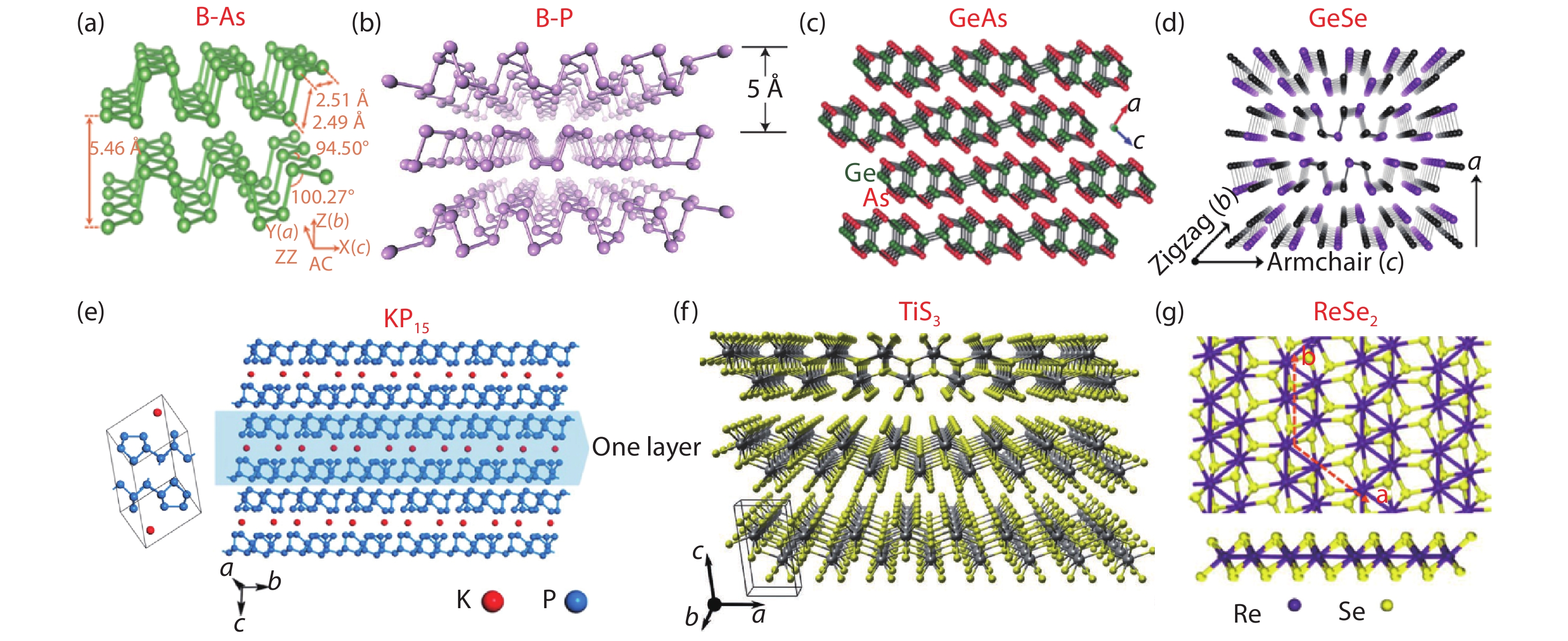
Fig. 1.  (Color online) Crystal structures of two-dimensional anisotropic materials, including (a) orthorhombic black-arsenic. Reproduced with permission[35]. Copyright 2018, John Wiley and Sons. (b) Orthorhombic black-phosphorus. Reproduced with permission[46]. Copyright 2014, Springer Nature. (c) Monoclinic GeAs. Reproduced with permission[47]. Copyright 2018, John Wiley and Sons. (d) Orthorhombic GeSe. Reproduced with permission[41]. Copyright 2017, American Chemical Society. (e) Triclinic KP15. Reproduced with permission[45]. Copyright 2018, American Chemical Society. (f) Monoclinic TiS3. Reproduced with permission[48]. Copyright 2018, Wiley-VCH. (g) Triclinic ReSe2. Reproduced with permission[49]. Copyright 2016, American Chemical Society.

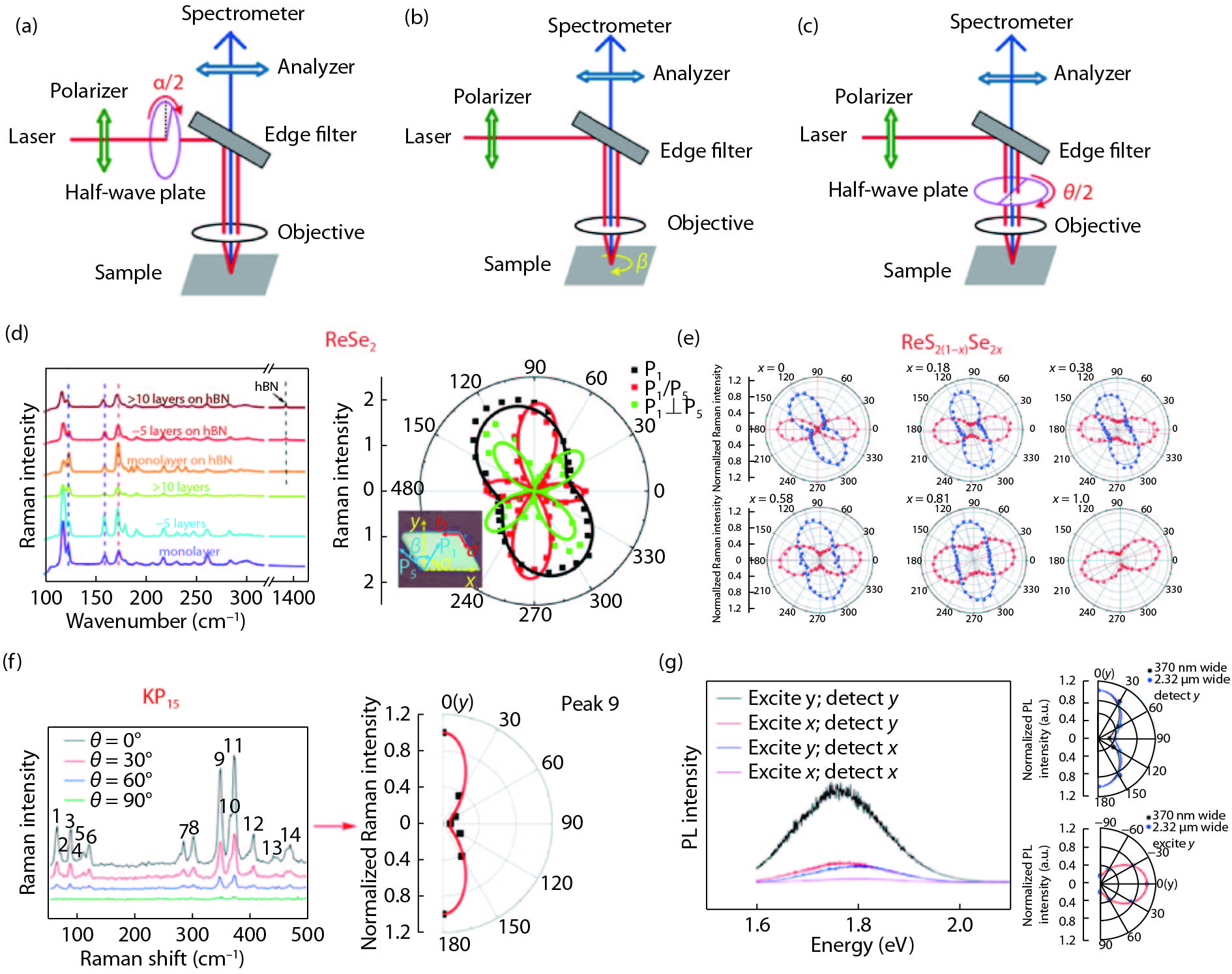
Fig. 2.  (Color online) Raman spectroscopy. (a)–(c) the schematic diagram of three typical polarized-Raman configurations. Reproduced with permission[62]. Copyright 2017, CPB. (d) The left is the Raman spectra of ReSe2 grown on hBN and SiO2 respectively. The right is the angular-dependent Raman intensity of 238 cm–1 shown in polar plot under different polarized-Raman configurations. Reproduced with permission[44]. Copyright 2018, American Chemical Society. (e) the angular-dependent Raman intensity of 212 and 406 cm–1 in ReS2(1–x)Se2x. Reproduced with permission[49]. Copyright 2016, American Chemical Society. (f) Angle-resolved polarized Raman spectra of KP15. The right picture is the intensity of peak 9. (g) Polarization-resolved PL intensity of KP15. The polar plots show the PL intensity of KP15 as the function of the detection angle and excitation angle respectively. Reproduced with permission[45]. Copyright 2018, American Chemical Society.

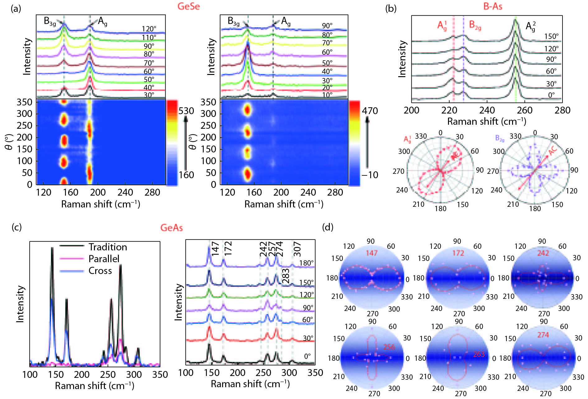
Fig. 3.  (Color online) (a) The angle-dependent Raman spectrum of GeSe and the corresponding contour color map in the parallel-polarization configuration (left) and cross-polarization configuration (right). Reproduced with permission[41]. Copyright 2017, American Chemical Society. (b) The Raman spectrum of B-As with laser polarized along different directions (up). The angle-resolved intensity of Ag1 and B2g-mode are extracted and shown in polar plot (down). Reproduced with permission[35]. Copyright 2018, John Wiley and Sons. (c) The Raman spectrum of GeAs in the non-polarized, parallel-polarized and cross-polarized configuration (left). The angle-dependent Raman spectrum of GeAs under traditional configuration (right). (d) The intensities of angle-dependent Raman peak are extracted and shown in the polar plot. Reproduced with permission[40]. Copyright 2018, American Chemical Society.

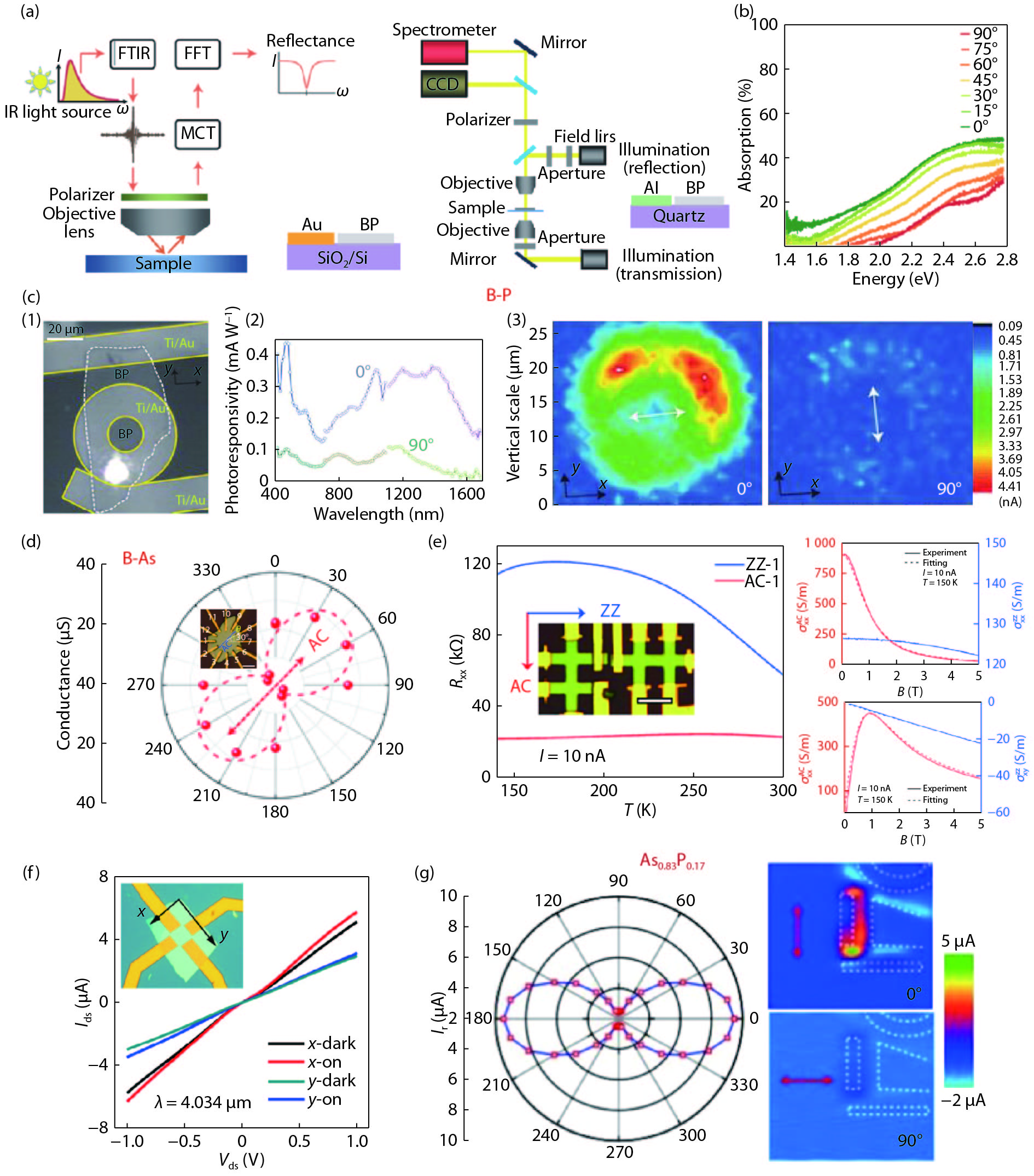
Fig. 4.  (Color online) (a) Schematic of the optical measurement under visible light (left-picture) and infrared light (right-picture). (b) Light absorption of B-P flake with different polarized light. (c) B-P photodetector with broadband response and polarization sensitivity. (1) The optical image of B-P photodetector with ring-electrode. (2) Polarization dependence of photoresponsivity from 400 to 1700 nm with polarization along x crystal axis (0°) and y crystal axis (90°). (3) The spatial mapping of photocurrent under polarization angle of 0 and 90 degree. Reproduced with permission[38]. Copyright 2015, Springer Nature. (d) The angle-dependent electrical conductance of B-As. The optical image of device for the anisotropic electrical measurements is inserted in it. (e) Temperature dependent resistance based on B-As Hall device shown in the inset(left). The magnetic field -dependent conductively ${\sigma _{xx}}$ and ${\sigma _{xy}}$, corresponding with the direction of armchair and zigzag (right). Reproduced with permission[35]. Copyright 2018, John Wiley and Sons. (f) The IdsVds curves of As0.83P0.17 with illumination and dark environment along x axis and y axis. (g) The laser polarization-sensitive photocurrents of As0.83P0.17 in polar plot at Vds = 0 V (left). Photocurrent mapping of As0.83P0.17 at Vds = 0 V (right) when polarization direction parallels (0°) and perpendicular (90°) to the contact edge of the metal. Reproduced with permission[39]. Copyright 2017, American Association for the Advancement of Science.

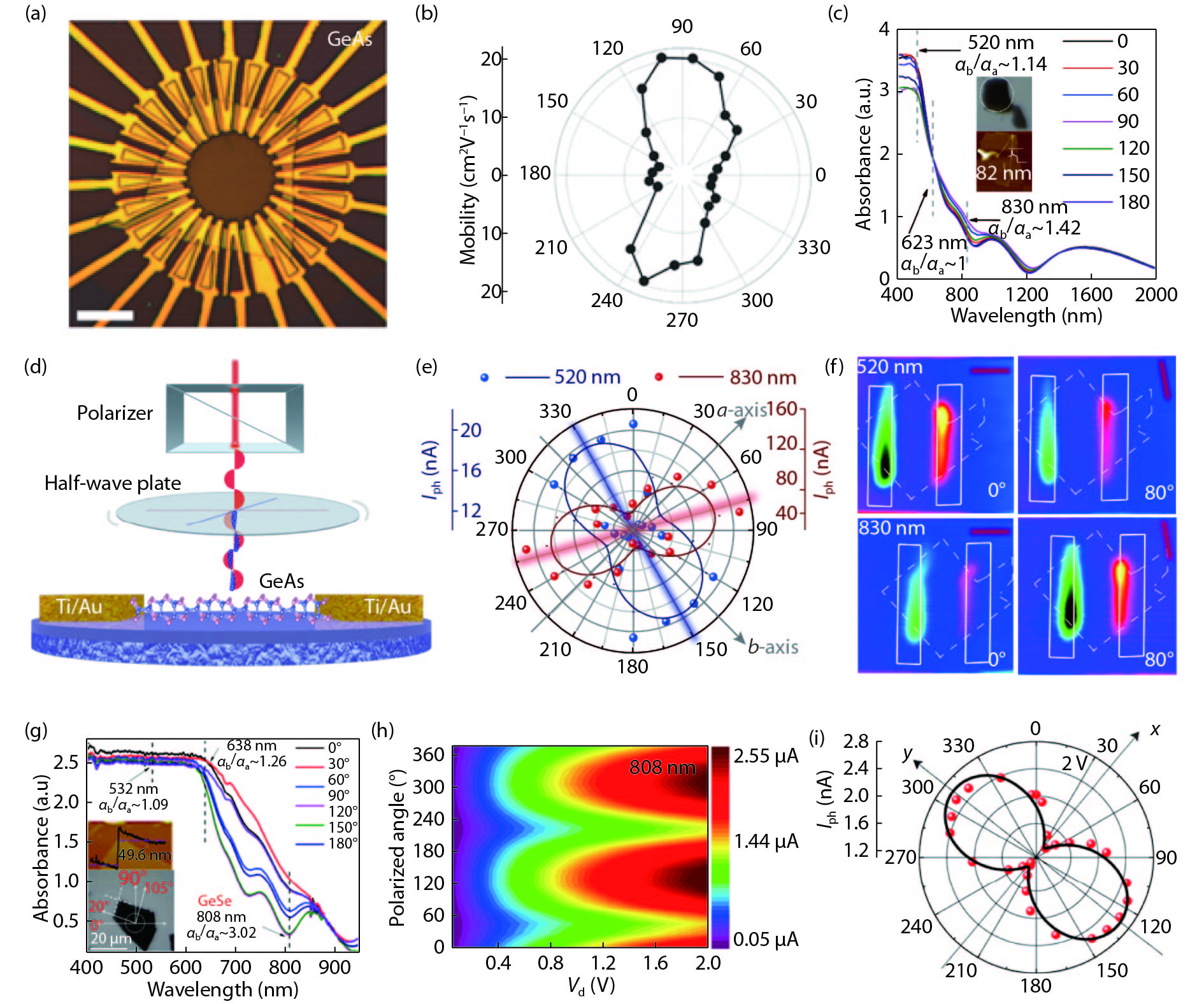
Fig. 5.  (Color online) The properties of electricity and photoelectricity. (a) The optical image of GeAs for angle-dependent transporting measurement. (b) The anisotropic field-effect mobility in polar plot. Reproduced with permission[47]. Copyright 2018, John Wiley and Sons. (c) Angle-resolved absorption spectra of GeAs from 400 to 2000 nm. (d) The schematic diagram of polarized photodetection devices. (e) The polarization-sensitive photocurrents in polar plot under 520 and 830 nm laser. (f) The mapping of polarization-dependent photocurrent under 520 and 830 nm laser. Reproduced with permission[40]. Copyright 2018, American Chemical Society. (g) Polarization-resolved experimental absorption spectra of GeSe from 400 to 950 nm. (h) The colormap of anisotropic photo response under the 808 nm laser. x-axis represents the voltage of source and drain, y-axis represents the polarized angle, and Iph is denoted by the color bar. (i) The data of polarized Iph are extracted and shown in polar plot. Reproduced with permission[41]. Copyright 2017, American Chemical Society.

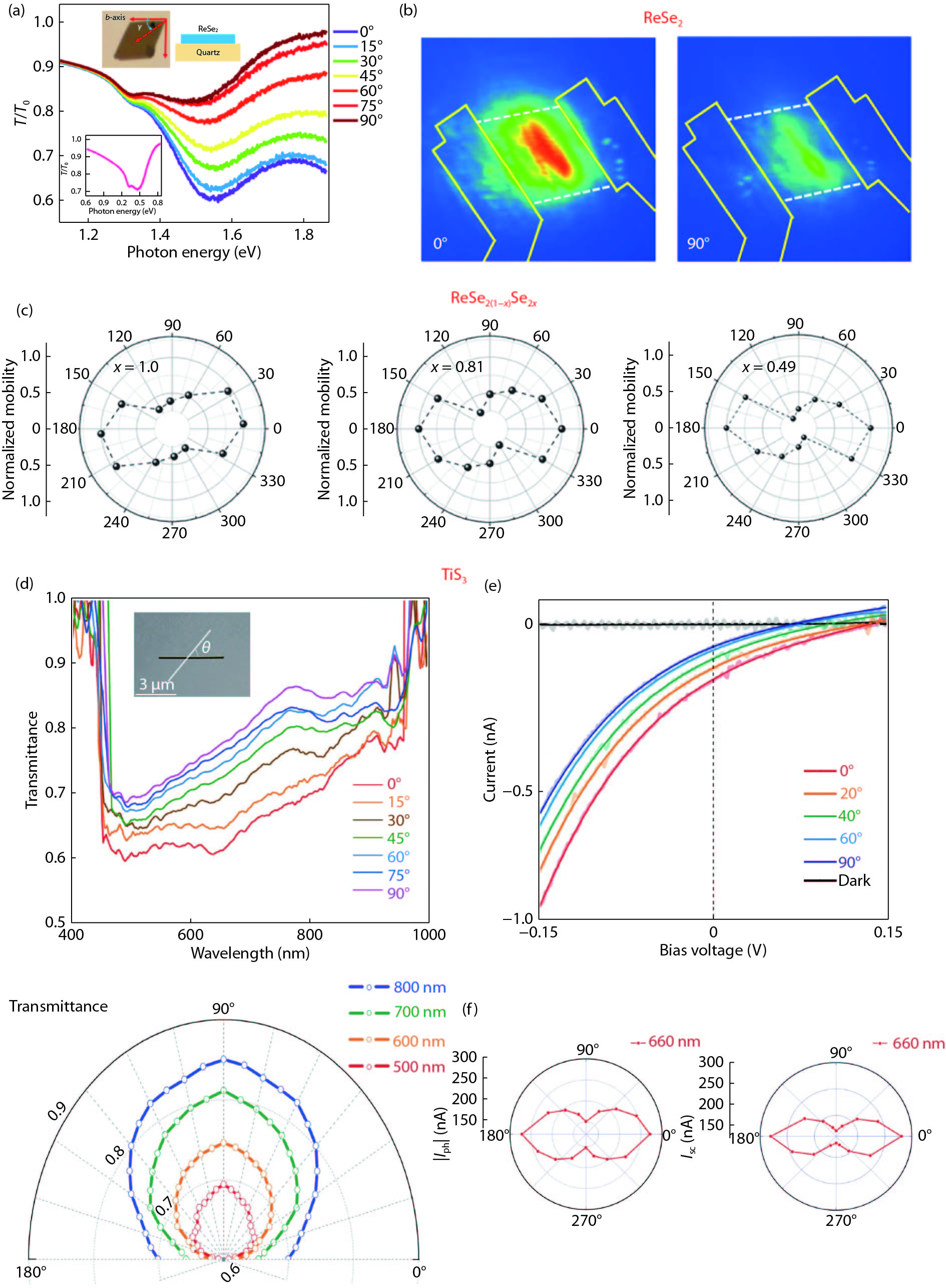
Fig. 6.  (Color online) (a) The polarization sensitive transmission spectra of ReSe2 nanoflake. (b) Polarization dependent photocurrent mapping based on ReSe2 FET. The thickness of the ReSe2 channel is 12 nm. Reproduced with permission[44]. Copyright 2016, American Chemical Society. (c) Angle-dependent mobility of ReSe2, ReS0.38Se1.62 and ReS1.02Se0.98 alloys. Reproduced with permission[48]. Copyright 2017, John Wiley and Sons. (d) The polarization-sensitive transmittance spectra of a TiS3 crystal from 400 to 1000 nm (up-picture). Polar plot of the transmittance at 500, 600, 700, 800 nm wavelengths (down-picture). (e) IV curves of the TiS3/Si-based device under the illumination of linearly polarized laser (660 nm). (f) Two polar plots of polarization-sensitive light currents under the bias voltage of –2 V (left-picture) and 0 V (right-picture). Reproduced with permission[48]. Copyright 2018, Wiley-VCH.

Table 1.   2D anisotropic materials and reported crystal system, space group, bandgap, responsivity and anisotropic dichroic ratio.

MaterialSystemSpace groupBandgap (bulk/ monolayer)ResponsivityDichroic ratioRef.
B-POrthorhombicP2/c2/0.3 eVN8.7 at 1550 nm[68, 69]
As0.83P0.17OrthorhombicPcmn-D182h0.15/- eV15–30 mA/W at MIR region3.88 at 1550 nm[39]
GeSeOrthorhombicPcmn-D2h 161.34/1.70 eV4.25 A/W2.16808 nm, 1.44638 nm 1.09 532 nm[41]
GeAsMonoclinicC2/m0.83/2.07 eVN1.49 at 520 nm, 4.4 at
808 nm
[40, 47]
GePMonoclinicC2/m0.51/1.68 eV3.1 A/W at 532 nm1.83 at 532 nm[31]
ReS2TriclinicP1(bar)1.62/1.52 eV16.14 A/W at 532 nm~4.0 at 532 nm[43]
ReSe2TriclinicP1(bar)1.31/1.26 eV1.5 mA/W at 633 nm~ 2.0 at 633 nm, ~ 2.0 at 520 nm[44]
TiS3MonoclinicP21/m1.1/N eVN~4.0 at 830 nm, ~4.6 at
638 nm, ~2.8 at 532 nm
[52]
TiSeTetragonalI4/mcm (D4h 18)0.73/- eV1.43A/W at 633 nm2.65 at 633 nm[70]
TeTrigonalD340.35/1 eV5.3 A/W at 1.5 μm, 3 A/W at
3.0 μm
1.43 at 1.5 μm, 6.0 at
3.0 μm
[15]
Td-TaIrTe4OrthorhombicPmn21Semimetal0.34 mA/W at 633 nm, 30.2 μA/W at 4 μm, 20 μA/W at 10.6 μm1.13 at 633 nm, 1.56 at 4 μm, 1.88 at 10.6 μm[71]
Td-MoTe2OrthorhombicPmn21Semimetal0.40 mA/W at 532nm, 0.0415 mA/W at 10.6 μm,1.19 at 638 nm, 1.92 at 4 μm, 2.72 at 10.6 μm[72]
Td-WTe2OrthorhombicPmn21Semimetal250 A/W at 3.8 μm under 77 K4.9 at 514.5 nm[73]
N: Not acquired.
DownLoad: CSV
[1]
Shang J, Huang L, Wei Z. Effects of vertical electric field and compressive strain on electronic properties of bilayer ZrS2. J Semicond, 2017, 38(3), 033001 doi: 10.1088/1674-4926/38/3/033001
[2]
Fan C, Li Y, Lu F, et al. Wavelength dependent UV–vis photodetectors from SnS2 flakes. RSC Adv, 2016, 6(1), 422 doi: 10.1039/C5RA24905H
[3]
Wei Z, Li B, Xia C, et al. Various structures of 2D transition-metal dichalcogenides and their applications. Small Methods, 2018, 2(11), 1800094 doi: 10.1002/smtd.v2.11
[4]
Wang X, Cui Y, Li T, et al. Recent advances in the functional 2D photonic and optoelectronic devices. Adv Opt Mater, 2018, 1801274 doi: 10.1002/adom.201801274
[5]
Wang Y, Huang L H, Li B, et al. Composition-tunable 2D SnSe2(1− x)S2 x alloys towards efficient bandgap engineering and high performance (opto)electronics. J Mater Chem C, 2017, 5(1), 84 doi: 10.1039/C6TC03751H
[6]
Mueller T, Xia F, Avouris P. Graphene photodetectors for high-speed optical communications. Nat Photon, 2010, 4, 297 doi: 10.1038/nphoton.2010.40
[7]
Novoselov K S, Geim A K, Morozov S V, et al. Two-dimensional gas of massless Dirac fermions in graphene. Nature, 2005, 438, 197 doi: 10.1038/nature04233
[8]
Huang L, Tao L, Gong K, et al. Role of defects in enhanced Fermi level pinning at interfaces between metals and transition metal dichalcogenides. Phys Rev B, 2017, 96, 205303 doi: 10.1103/PhysRevB.96.205303
[9]
Podzorov V, Gershenson M, Zeis C, et al. High-mobility field-effect transistors based on transition metal dichalcogenides. Appl Phys Lett, 2004, 84, 3301-3303 doi: 10.1063/1.1723695
[10]
Xia C, Li J. Recent advances in optoelectronic properties and applications of two-dimensional metal chalcogenides. J Semicond, 2016, 37(5), 051001 doi: 10.1088/1674-4926/37/5/051001
[11]
Huo N, Yang Y, Li J. Optoelectronics based on 2D TMDs and heterostructures. J Semicond, 2017, 38(3), 031002 doi: 10.1088/1674-4926/38/3/031002
[12]
Tan Q H, Zhang X, Luo X D, et al. Layer-number dependent high-frequency vibration modes in few-layer transition metal dichalcogenides induced by interlayer couplings. J Semicond, 2017, 38(3), 031006 doi: 10.1088/1674-4926/38/3/031006
[13]
Lou Z, Liang Z, Shen G. Photodetectors based on two dimensional materials. J Semicond, 2016, 37(9), 091001 doi: 10.1088/1674-4926/37/9/091001
[14]
Amani M, Regan E, Bullock J, et al. Mid-wave infrared photoconductors based on black phosphorus-arsenic alloys. ACS Nano, 2017, 11(11), 11724 doi: 10.1021/acsnano.7b07028
[15]
Amani M, Tan C, Zhang G, et al. Solution-synthesized high-mobility tellurium nanoflakes for short-wave infrared photodetectors. ACS Nano, 2018, 12(7), 7253 doi: 10.1021/acsnano.8b03424
[16]
Chu F, Chen M, Wang Y, et al. A highly polarization sensitive antimonene photodetector with a broadband photoresponse and strong anisotropy. J Mater Chem C, 2018, 6(10), 2509 doi: 10.1039/C7TC05488B
[17]
Hong T, Chamlagain B, Lin W, et al. Polarized photocurrent response in black phosphorus field-effect transistors. Nanoscale, 2014, 6, 8978 doi: 10.1039/C4NR02164A
[18]
Huo N, Yang S, Wei Z, et al. Photoresponsive and gas sensing field-effect transistors based on multilayer WS(2) nanoflakes. Sci Rep, 2014, 4, 5209 doi: 10.1038/srep05209
[19]
Lai J, Liu X, Ma J, et al. Anisotropic broadband photoresponse of layered type-II Weyl semimetal MoTe2. Adv Mater, 2018, 30(22), e1707152 doi: 10.1002/adma.v30.22
[20]
Li Y, Wang Y, Huang L, et al. Anti-ambipolar field-effect transistors based on few-layer 2D transition metal dichalcogenides. ACS Appl Mater Interfaces, 2016, 8(24), 15574 doi: 10.1021/acsami.6b02513
[21]
Wang Y, Huang L, Wei Z. Photoresponsive field-effect transistors based on multilayer SnS2 nanosheets. J Semicond, 2017, 38(3), 034001 doi: 10.1088/1674-4926/38/3/034001
[22]
Cao T, Li Z, Qiu D Y, et al. Gate switchable transport and optical anisotropy in 90 degrees twisted bilayer black phosphorus. Nano Lett, 2016, 16(9), 5542 doi: 10.1021/acs.nanolett.6b02084
[23]
Liu B, Kopf M, Abbas A N, et al. Black arsenic-phosphorus: layered anisotropic infrared semiconductors with highly tunable compositions and properties. Adv Mater, 2015, 27, 4423 doi: 10.1002/adma.v27.30
[24]
Zhong M, Wang X, Liu S, et al. High-performance photodetectors based on Sb2S3 nanowires: wavelength dependence and wide temperature range utilization. Nanoscale, 2017, 9, 12364 doi: 10.1039/C7NR03574H
[25]
Ye L, Wang P, Luo W, et al. Highly polarization sensitive infrared photodetector based on black phosphorus-on-WSe2 photogate vertical heterostructure. Nano Energy, 2017, 37, 53 doi: 10.1016/j.nanoen.2017.05.004
[26]
Zhong M, Zhou K, Wei Z, et al. Highly anisotropic solar-blind UV photodetector based on large-size two-dimensional α-MoO3 atomic crystals. 2D Mater, 2018, 5, 035033 doi: 10.1088/2053-1583/aac65e
[27]
Li J B, Wang X R. Preface to the special topic on 2D materials and devices. J Semicond, 2017, 38(3), 031001 doi: 10.1088/1674-4926/38/3/031001
[28]
Hu Z, Li Q, Lei B, et al. Abnormal near-infrared absorption in 2D black phosphorus induced by Ag nanoclusters surface functionalization. Adv Mater, 2018, 1801931 doi: 10.1002/adma.201801931
[29]
Lin T, Cong X, Lin M L, et al. The phonon confinement effect in two-dimensional nanocrystals of black phosphorus with anisotropic phonon dispersions. Nanoscale, 2018, 10(18), 8704 doi: 10.1039/C8NR01531G
[30]
Barreteau C, Michon B, Besnard C, et al. High-pressure melt growth and transport properties of SiP, SiAs, GeP, and GeAs 2D layered semiconductors. J Cryst Growth, 2016, 443, 75 doi: 10.1016/j.jcrysgro.2016.03.019
[31]
Li L, Wang W, Gong P, et al. 2D GeP: An unexploited low-symmetry semiconductor with strong In-plane anisotropy. Adv Mater, 2018, 30(14), e1706771 doi: 10.1002/adma.v30.14
[32]
Mortazavi B, Rabczuk T. Anisotropic mechanical properties and strain tuneable band-gap in single-layer SiP, SiAs, GeP and GeAs. Physica E, 2018, 103, 273 doi: 10.1016/j.physe.2018.06.011
[33]
Li C, Wang S, Li C, et al. Highly sensitive detection of polarized light using a new group IV–V 2D orthorhombic SiP. J Mater Chem C, 2018, 6(27), 7219 doi: 10.1039/C8TC02037J
[34]
Wang X, Jones A, Seyler K, et al. Highly anisotropic and robust excitons in monolayer black phosphorus. Nat Nanotechnol, 2015, 10, 517 doi: 10.1038/nnano.2015.71
[35]
Chen Y, Chen C, Kealhofer R, et al. Black arsenic: a layered semiconductor with extreme in-plane anisotropy. Adv Mater, 2018, 30, 1800754 doi: 10.1002/adma.v30.30
[36]
Zhong M, Xia Q, Pan L, et al. Thickness-dependent carrier transport characteristics of a new 2D elemental semiconductor: black arsenic. Adv Funct.Mater, 2018, 28, 1802581 doi: 10.1002/adfm.201802581
[37]
Silva-Guillén J A, Canadell E, Ordejón P, et al. Anisotropic features in the electronic structure of the two-dimensional transition metal trichalcogenide TiS3: electron doping and plasmons. 2D Mater, 2017, 4(2), 025085 doi: 10.1088/2053-1583/aa6b92
[38]
Yuan H, Liu X, Afshinmanesh F, et al. Polarization-sensitive broadband photodetector using a black phosphorus vertical p–n junction. Nat Nanotechnol, 2015, 10, 707 doi: 10.1038/nnano.2015.112
[39]
Long M, Gao A, Wang P, et al. Room temperature high-detectivity mid-infrared photodetectors based on black arsenic phosphorus. Sci Adv, 2017, 3, e1700589 doi: 10.1126/sciadv.1700589
[40]
Zhou Z, Long M, Pan L, et al. Perpendicular optical reversal of the linear dichroism and polarized photodetection in 2D GeAs. ACS Nano, 2018 doi: 10.1021/acsnano.8b06629
[41]
Wang X, Li Y, Huang L, et al. Short-wave near-infrared linear dichroism of two-dimensional germanium selenide. J Am Chem Soc, 2017, 139, 14976 doi: 10.1021/jacs.7b06314
[42]
Lin Y C, Komsa H P, Yeh C H, et al. Single-layer ReS(2): two-dimensional semiconductor with tunable in-plane anisotropy. ACS Nano, 2015, 9(11), 11249 doi: 10.1021/acsnano.5b04851
[43]
Zhang E, Jin Y, Yuan X, et al. ReS2-based field-effect transistors and photodetectors. Adv Funt Mater, 2015, 25, 4076 doi: 10.1002/adfm.v25.26
[44]
Zhang E, Wang P, Li Z, et al. Tunable ambipolar polarization-sensitive photodetectors based on high-anisotropy ReSe2 nanosheets. ACS Nano, 2016, 10, 8067 doi: 10.1021/acsnano.6b04165
[45]
Tian N, Yang Y, Liu D, et al. High anisotropy in tubular layered exfoliated KP15. ACS Nano, 2018, 12(2), 1712 doi: 10.1021/acsnano.7b08368
[46]
Li L, Yu Y, Ye GJ, et al. Black phosphorus field-effect transistors. Nat Nanotechnol, 2014, 9(5), 372 doi: 10.1038/nnano.2014.35
[47]
Guo J, Liu Y, Ma Y, et al. Few-layer GeAs field-effect transistors and infrared photodetectors. Adv Mater, 2018, 30, 1705934 doi: 10.1002/adma.201705934
[48]
Niu Y, Frisenda R, Flores E, et al. Polarization-sensitive and broadband photodetection based on a mixed-dimensionality TiS3/Si p–n junction. Adv Optical Mater, 2018, 6(19), 1800351 doi: 10.1002/adom.v6.19
[49]
Wen W, Zhu Y, Liu X, et al. Anisotropic spectroscopy and electrical properties of 2D ReS2(1– x)Se2 x. alloys with distorted 1T structure. Small, 2017, 13(12), 1603788 doi: 10.1002/smll.201603788
[50]
Rau J W, Kannewurf C R. Optical absorption, reflectivity, and electrical conductivity in GeAs and GeAs2. Phys Rev B, 1971, 3, 2581 doi: 10.1103/PhysRevB.3.2581
[51]
Wang P, Liu S, Luo W, et al. Arrayed Van Der Waals broadband detectors for dual-band detection. Adv Mater, 2017, 29(16) doi: 10.1002/adma.201604439
[52]
Liu S, Xiao W, Zhong M, et al. Highly polarization sensitive photodetectors based on quasi-1D titanium trisulfide (TiS3). Nanotechnology, 2018, 29(18), 184002 doi: 10.1088/1361-6528/aaafa2
[53]
Rahman M, Davey K, Qiao S Z. Advent of 2D rhenium disulfide (ReS2): fundamentals to applications. Adv Funct Mater, 2017, 27(10), 1606129 doi: 10.1002/adfm.v27.10
[54]
Kang B, Kim Y, Cho JH, et al. Ambipolar transport based on CVD-synthesized ReSe2. 2D Mater, 2017, 4(2), 025014 doi: 10.1088/2053-1583/aa591f
[55]
Zhang X, Tan Q H, Wu J B, et al. Review on the Raman spectroscopy of different types of layered materials. Nanoscale, 2016, 8(12), 6435 doi: 10.1039/C5NR07205K
[56]
Yang G, Zhang W. Renaissance of pyridine-oxazolines as chiral ligands for asymmetric catalysis. Chem Soc Rev, 2018, 47(5), 1783 doi: 10.1039/C7CS00615B
[57]
Wu J B, Zhao H, Li Y, et al. Monolayer molybdenum disulfide nanoribbons with high optical anisotropy. Adv Opt Mater, 2016, 4(5), 756 doi: 10.1002/adom.v4.5
[58]
Wu J B, Lin M L, Cong X, et al. Raman spectroscopy of graphene-based materials and its applications in related devices. Chem Soc Rev, 2018, 47(5), 1822 doi: 10.1039/C6CS00915H
[59]
Liang L, Zhang J, Sumpter B G, et al. Low-frequency shear and layer-breathing modes in Raman scattering of two-dimensional materials. ACS Nano, 2017, 11(12), 11777 doi: 10.1021/acsnano.7b06551
[60]
Zhao H, Wu J, Zhong H, et al. Interlayer interactions in anisotropic atomically thin rhenium diselenide. Nano Res, 2015, 8(11), 3651 doi: 10.1007/s12274-015-0865-0
[61]
Ribeiro H B, Pimenta M A, de Matos C J S. Raman spectroscopy in black phosphorus. J Raman Spectrosc, 2018, 49(1), 76 doi: 10.1002/jrs.v49.1
[62]
Liu X L, Zhang X, Lin M L, et al. Different angle-resolved polarization configurations of Raman spectroscopy: A case on the basal and edge plane of two-dimensional materials. Chin Phys B, 2017, 26(6), 067802 doi: 10.1088/1674-1056/26/6/067802
[63]
Lee K, Kamali S, Ericsson T, et al. GeAs: Highly anisotropic van der Waals thermoelectric material. Chem Mater, 2016, 28(8), 2776 doi: 10.1021/acs.chemmater.6b00567
[64]
Zhou L, Guo Y, Zhao J. GeAs and SiAs monolayers: novel 2D semiconductors with suitable band structures. Phys E, 2018, 95, 149 doi: 10.1016/j.physe.2017.08.016
[65]
Song Q, Wang H, Pan X, et al. Anomalous in-plane anisotropic Raman response of monoclinic semimetal 1 T -MoTe2. Sci Rep, 2017, 7(1), 1758 doi: 10.1038/s41598-017-01874-2
[66]
Song Q, Wang H, Xu X, et al. The polarization-dependent anisotropic Raman response of few-layer and bulk WTe2 under different excitation wavelengths. RSC Adv, 2016, 6(105), 103830 doi: 10.1039/C6RA23687A
[67]
Xu X, Song Q, Wang H, et al. In-plane anisotropies of polarized raman response and electrical conductivity in layered tin selenide. ACS Appl Mater Interfaces, 2017, 9(14), 12601 doi: 10.1021/acsami.7b00782
[68]
Liu X, Ryder C R, Wells S A, et al. Resolving the in-plane anisotropic properties of black phosphorus. Small Methods, 2017, 1, 1700143 doi: 10.1002/smtd.201700143
[69]
Venuthurumilli P, Ye P, Xu X. Plasmonic resonance enhanced polarization-sensitive photodetection by black phosphorus in near infrared. ACS Nano, 2018, 12, 4861 doi: 10.1021/acsnano.8b01660
[70]
Niu C, Buhl P M, Bihlmayer G, et al. Two-dimensional topological crystalline insulator and topological phase transition in TlSe and TlS monolayers. Nano Lett, 2015, 15(9), 6071 doi: 10.1021/acs.nanolett.5b02299
[71]
Lai J, Liu Y, Ma J, et al. Broadband anisotropic photoresponse of the "hydrogen atom" version type-II Weyl semimetal candidate TaIrTe4. ACS Nano, 2018, 12(4), 4055 doi: 10.1021/acsnano.8b01897
[72]
Jiang J, Liu Z K, Sun Y, et al. Signature of type-II Weyl semimetal phase in MoTe2. Nat Commun, 2017, 8, 13973 doi: 10.1038/ncomms13973
[73]
Zhou W, Chen J, Gao H, et al. Anomalous and polarization-sensitive photoresponse of Td–WTe2 from visible to infrared light. Adv Mater, 2019, 31(5), e1804629 doi: 10.1002/adma.201804629
[74]
Xia F, Wang H, Jia Y. Rediscovering black phosphorus as an anisotropic layered material for optoelectronics and electronics. Nat Commun, 2014, 5, 4458 doi: 10.1038/ncomms5458
[75]
Cui F, Feng Q, Hong J, et al. Synthesis of large-size 1T' ReS2 xSe2(1– x) alloy monolayer with tunable bandgap and carrier type. Adv Mater, 2017, 29(46), 1705015 doi: 10.1002/adma.201705015
[76]
Meng X, Zhou Y, Chen K, et al. Anisotropic saturable and excited-state absorption in bulk ReS2. Adv Opt Mater, 2018, 6(14), 1800137 doi: 10.1002/adom.201800137
[77]
Zheng H, Zhu M, Zhang J, et al. A first-principles study on the magnetic properties of Sc, V, Cr and Mn-doped monolayer TiS3. RSC Adv, 2016, 6(60), 55194 doi: 10.1039/C6RA06486H
[78]
Li L, Gong P, Wang W, et al. Strong in-plane anisotropies of optical and electrical response in layered dimetal chalcogenide. ACS Nano, 2017, 11(10), 10264 doi: 10.1021/acsnano.7b04860
  • Search

    Advanced Search >>

    GET CITATION

    shu

    Export: BibTex EndNote

    Article Metrics

    Article views: 7819 Times PDF downloads: 520 Times Cited by: 0 Times

    History

    Received: 26 March 2019 Revised: 30 April 2019 Online: Accepted Manuscript: 15 May 2019Uncorrected proof: 15 May 2019Published: 05 June 2019

    Catalog

      Email This Article

      User name:
      Email:*请输入正确邮箱
      Code:*验证码错误
      Ziqi Zhou, Yu Cui, Ping-Heng Tan, Xuelu Liu, Zhongming Wei. Optical and electrical properties of two-dimensional anisotropic materials[J]. Journal of Semiconductors, 2019, 40(6): 061001. doi: 10.1088/1674-4926/40/6/061001 ****Z Q Zhou, Y Cui, P H Tan, X L Liu, Z M Wei, Optical and electrical properties of two-dimensional anisotropic materials[J]. J. Semicond., 2019, 40(6): 061001. doi: 10.1088/1674-4926/40/6/061001.
      Citation:
      Ziqi Zhou, Yu Cui, Ping-Heng Tan, Xuelu Liu, Zhongming Wei. Optical and electrical properties of two-dimensional anisotropic materials[J]. Journal of Semiconductors, 2019, 40(6): 061001. doi: 10.1088/1674-4926/40/6/061001 ****
      Z Q Zhou, Y Cui, P H Tan, X L Liu, Z M Wei, Optical and electrical properties of two-dimensional anisotropic materials[J]. J. Semicond., 2019, 40(6): 061001. doi: 10.1088/1674-4926/40/6/061001.

      Optical and electrical properties of two-dimensional anisotropic materials

      doi: 10.1088/1674-4926/40/6/061001
      More Information
      • Corresponding author: Email: liuxuelu@semi.ac.cn and zmwei@semi.ac.cn; Email: liuxuelu@semi.ac.cn and zmwei@semi.ac.cn
      • Received Date: 2019-03-26
      • Revised Date: 2019-04-30
      • Published Date: 2019-06-01

      Catalog

        /

        DownLoad:  Full-Size Img  PowerPoint
        Return
        Return