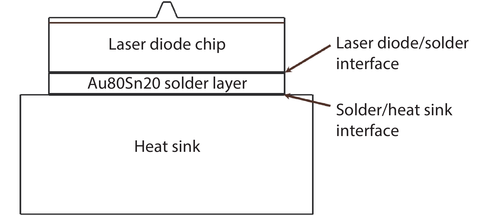
Fig. 1.
The schematic diagram of structure of packaged laser diodes.
ARTICLES
Hao Lin1, 2, Deyao Li2, Liqun Zhang2, Pengyan Wen2, Shuming Zhang2, Jianping Liu2, and Hui Yang2
Corresponding author: Jianping Liu, Email: jpliu2010@sinano.ac.cn
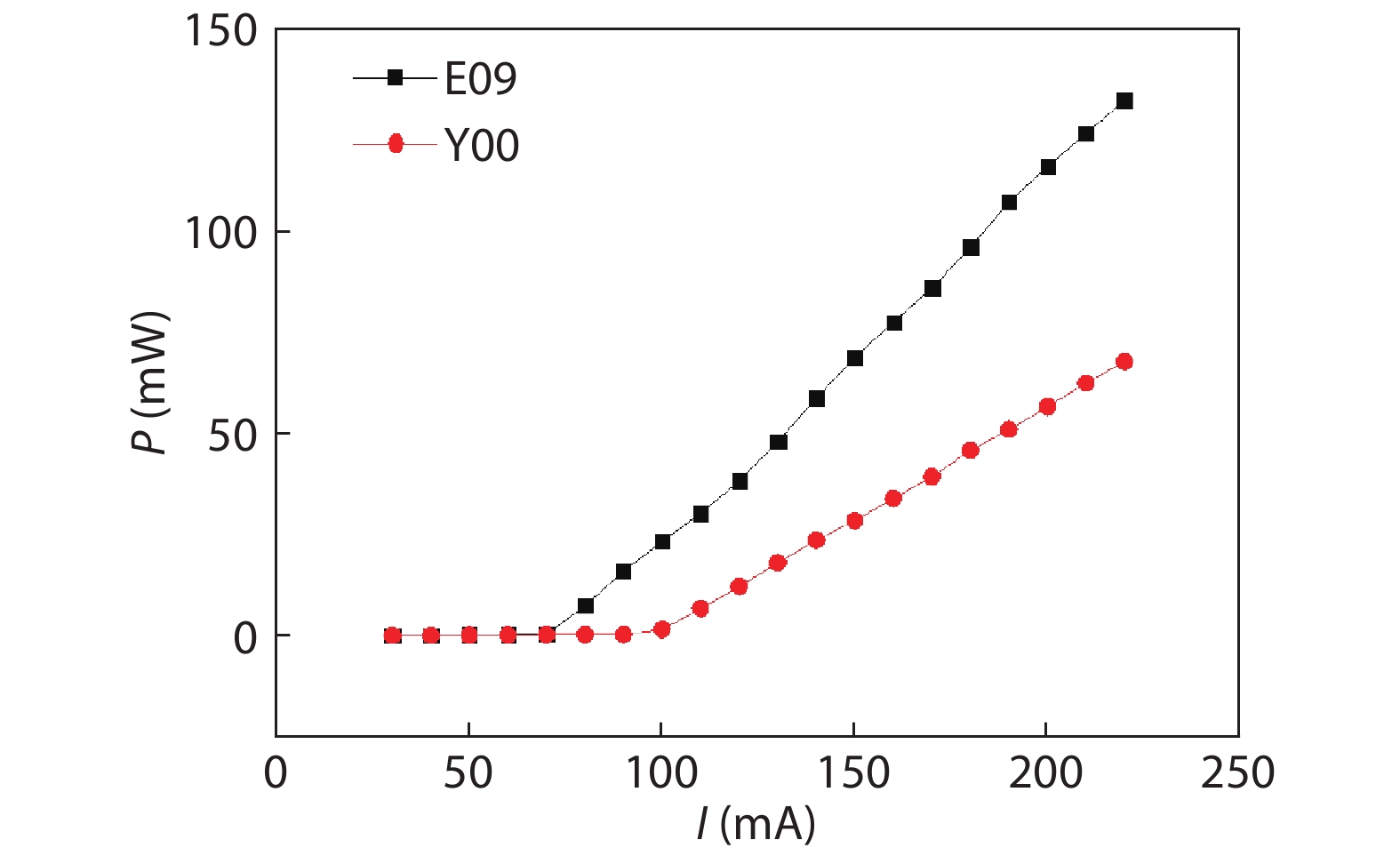
Abstract: Au80Sn20 alloy is a widely used solder for laser diode packaging. In this paper, the thermal resistance of GaN-based blue laser diodes packaged in TO56 cans were measured by the forward voltage method. The microstructures of Au80Sn20 solder were then investigated to understand the reason for the difference in thermal resistance. It was found that the microstructure with a higher content of Au-rich phase in the center of the solder and a lower content of (Au,Ni)Sn phase at the interface of the solder/heat sink resulted in lower thermal resistance. This is attributed to the lower thermal resistance of Au-rich phase and higher thermal resistance of (Au,Ni)Sn phase.
Keywords: Au80Sn20, laser diodes package, thermal resistance
| [1] |
Lee C C, Chien D H. Thermal and package design of high power laser diodes. Proc IEEE SEMI-THERM Symp, 1993, 75
|
| [2] |
Haque S, Steigerwald D, Rudaz S, et al. Packaging challenges of high-power LEDs for solid state lighting. Proc 36th Int Symp Microelectron, Boston, MA, 2003, 93
|
| [3] |
Elger G, Schmid M, Hanß A, et al. Analysis of new direct on PCB board attached high power flip-chip LEDs. 2015 IEEE 65th Electronic Components and Technology Conference (ECTC), 2015, 1310
|
| [4] |
Huang F F, Huang M L. Complexation behavior and co-electrodeposition mechanism of Au–Sn alloy in highly stable non-cyanide bath. J Electrochem Soc, 2018, 165(3), D152 doi: 10.1149/2.0721803jes
|
| [5] |
Zhu Z X, Li C C, Liao L L, et al. Au–Sn bonding material for the assembly of power integrated circuit module. J Alloys Compd, 2016, 671, 340e345 doi: 10.1016/j.jallcom.2016.02.065
|
| [6] |
Liu S F, Zhang D X, Xiong J R, et al. Microstructure evolution and properties of rapidly solidified Au-20Sn eutectic solder prepared by single-roll technology. J Alloys Compd, 2019, 781, 873e882 doi: 10.1016/j.jallcom.2018.12.073
|
| [7] |
Zeng G, McDonald S, Nogita K. Development of high-temperature solders: review. Microelectron Reliab, 2012, 52, 1306e1322 doi: 10.1016/j.microrel.2012.02.018
|
| [8] |
Zhang H, Minter J, Lee N C. A brief review on high-temperature, Pb-free die-attach materials. J Electr Mater, 2019, 48, 201 doi: 10.1007/s11664-018-6707-6
|
| [9] |
Dua C W, Soler R, Völker B, et al. Au–Sn solders applied in transient liquid phase bonding: Microstructure and mechanical behavior. Materialia, 2019, 8, 100503 doi: 10.1016/j.mtla.2019.100503
|
| [10] |
Doesburg J, Ivey D G. Microstructure and preferred orientation of Au–Sn alloy plated deposits. Mater Sci Eng B, 2000, 78, 44 doi: 10.1016/S0921-5107(00)00515-8
|
| [11] |
Wen P Y, Li D Y, Zhang S M, et al. High accuracy thermal resistance measurement in GaN/InGaN laser diodes. Solid-State Electron, 2015, 106, 50 doi: 10.1016/j.sse.2015.01.003
|
| [12] |
Kim D S, Holloway C, Han B T, et al. Method for predicting junction temperature distribution in a high-power laser diode bar. Appl Opt, 2016, 55, 7487 doi: 10.1364/AO.55.007487
|
| [13] |
Qiao Y B, Feng S W, Xiong C, et al. The thermal properties of AlGaAs/GaAs laser diode bars analyzed by the transient thermal technique. Solid-State Electron, 2013, 79, 192 doi: 10.1016/j.sse.2012.07.007
|
| [14] |
Liu Y T, Cao Q, Song G F, et al. The junction temperature and forward voltage relationship of GaN-based laser diode. Laser Phys, 2009, 19(3), 400 doi: 10.1134/S1054660X09030074
|
| [15] |
Xi Y, Xi J Q, Gessmann T, et al. Junction and carrier temperature measurements in deep-ultraviolet light-emitting diodes using three different methods. Appl Phys Lett, 2005, 86(3), 031907 doi: 10.1063/1.1849838
|
| [16] |
Min K J, Seungtaek K, Bok K S, et al. An analysis of transient thermal properties for high power GaN-based laser diodes. Phys Status Solidi C, 2010, 7(8), 1801 doi: 10.1002/pssc.200983498
|
| [17] |
Wen P Y, Li D Y, Zhang S M, et al. Identification of degradation mechanisms based on thermal characteristics of InGaN/GaN laser diodes. IEEE J Sel Top Quantum Electron, 2015, 21, 1500506 doi: 10.1109/JSTQE.2014.2372051
|
| [18] |
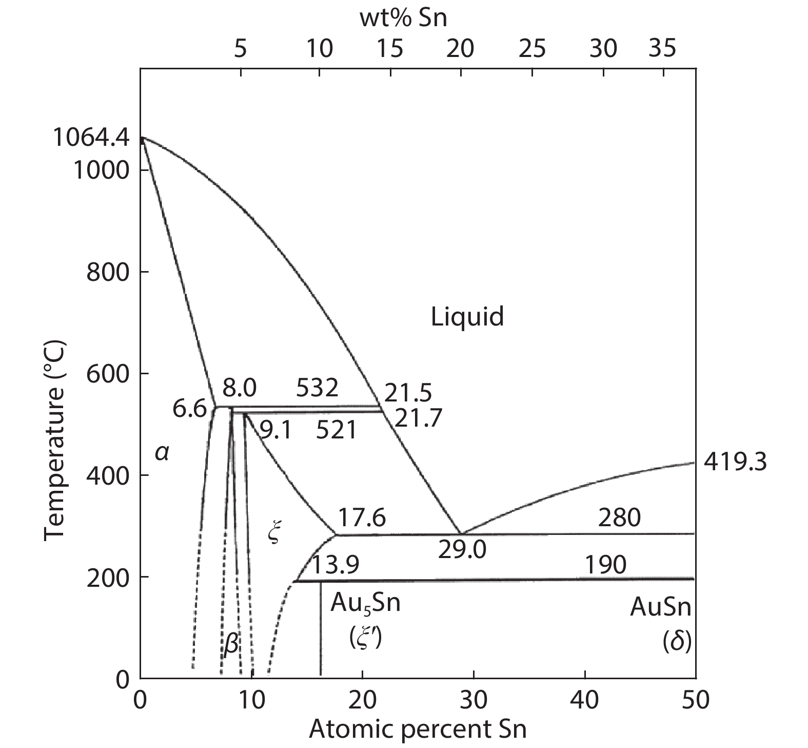
Ciulik J, Notis M R. The Au–Sn phase diagram. J Alloys Compnd, 1993, 191, 71 doi: 10.1016/0925-8388(93)90273-P
|
| [19] |
Teo J W R, Ng F L, Goi L S K, et al. Microstructure of eutectic 80Au/20Sn solder joint in laser diode package. Microelectron Eng, 2008, 85, 512 doi: 10.1016/j.mee.2007.09.009
|
| [20] |
Chung H M, Chen C M, Lin C P, et al. Microstructural evolution of the Au-20 wt.% Sn solder on the Cu substrate during reflow. J Alloys Compd, 2009, 485, 219 doi: 10.1016/j.jallcom.2009.06.018
|
| [21] |
Bergmann R, Tang P T, Hansen H N, et al. In-situ investigation of lead-free solder alloy formation using a hot-plate microscope. Proc 9th Electronics Packaging Technology Conference, 2007
|
| [22] |
Hsiao T C, Lin A D, Chan W Y. Laser soldered eutectic die-bonding processes in LED packaging. Sens Mater, 2016, 28, 409
|
| [23] |
Yoon S W, Choi W K, Lee H M. Improving the performance of lead-free solder reinforced with multi-walled carbon nanotubes. Scripta Mater, 1999, 40, 297 doi: 10.1016/S1359-6462(98)00417-5
|
| [24] |
Javid N S, Sayyadi R, Khodabakhshi F. Lead-free Sn-based/MW-CNTs nanocomposite soldering: effects of reinforcing content, Ni-coating modification, and isothermal ageing treatment. J Mater Sci: Mater Electron, 2019, 30, 4737 doi: 10.1007/s10854-019-00767-6
|
| [25] |
Shi X Q, Kwan H F, Nai S M L, et al. Kinetics of interface reaction and intermetallics growth of Sn-3.5Ag-0.7Cu/Au/Ni/Cu system under isothermal aging. J Mater Sci Lett, 2004, 39, 1095 doi: 10.1023/B:JMSC.0000012953.36499.73
|
| [26] |
Tan Q B, Deng C, Mao Y, et al. Evolution of primary phases and high-temperature compressive behaviors of as-cast AuSn20 alloys prepared by different solidification pathways. Gold Bull, 2011, 44, 27 doi: 10.1007/s13404-011-0004-y
|
| [27] |
Ronnie T J, Patil D S. Advances in high-power laser diode packaging. Semiconductor Laser Diode Technology and Applications, 2012, 321
|
| [28] |
Teo J W R, Shi X Q, Li G Y, et al. Modified face-down bonding of ridge-waveguide lasers using hard solder. IEEE Trans Electron Pack Manuf, 2008, 31, 159 doi: 10.1109/TEPM.2008.919329
|
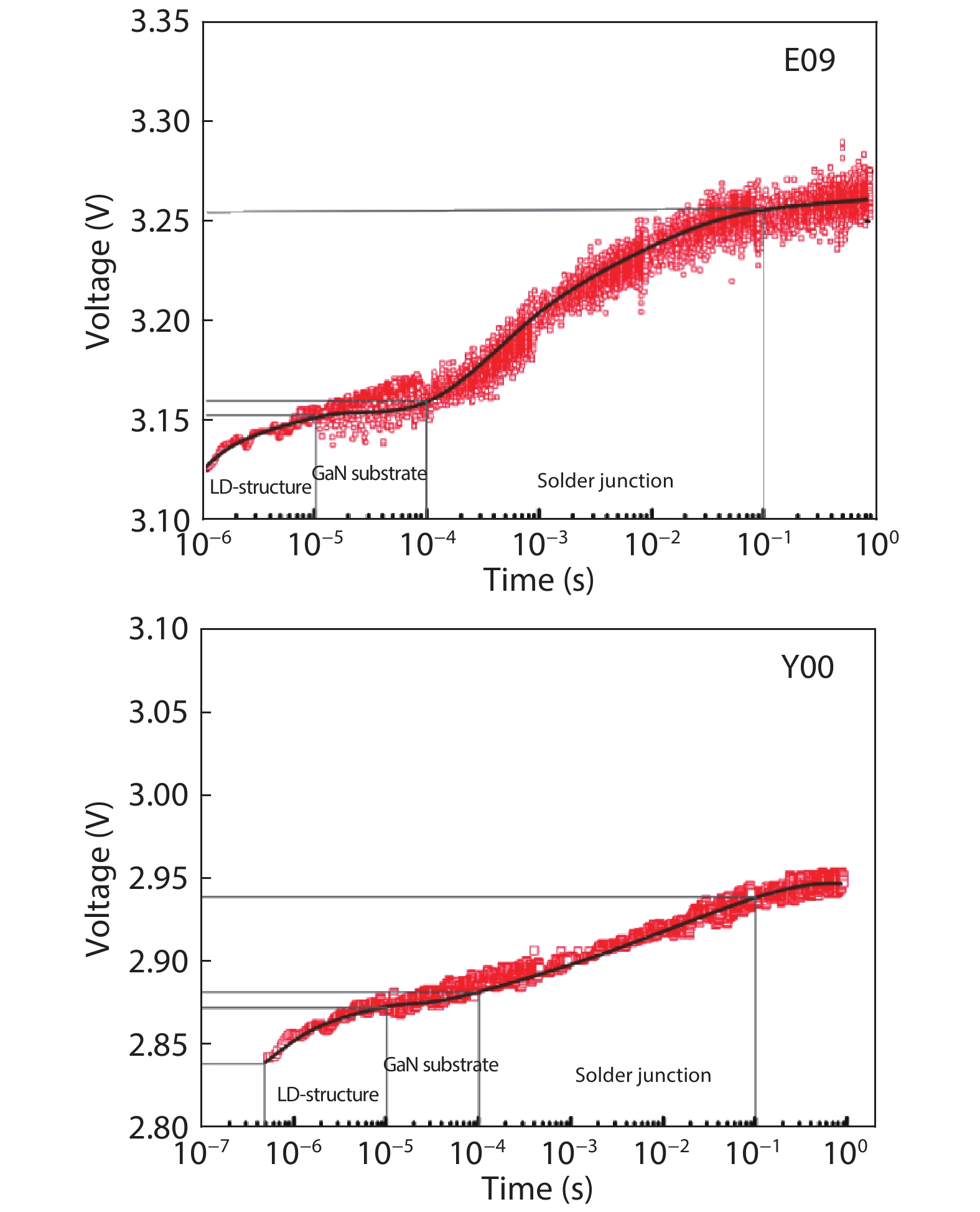
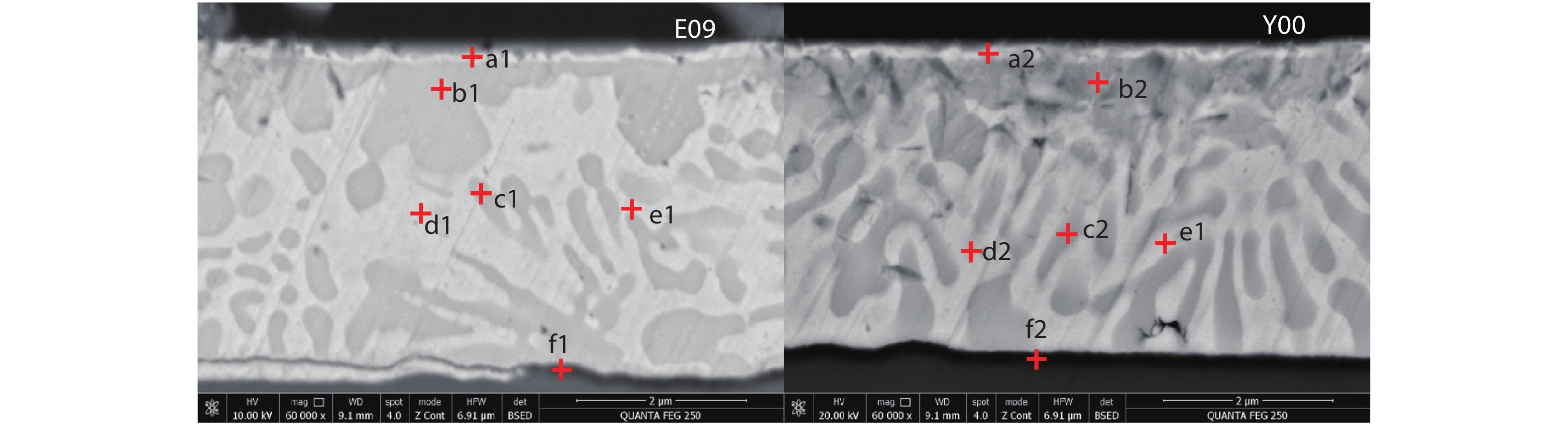
Table 1. Parameters of thermal resistance calculation.
| Sample | A (mV/K) | Vf0–Vft (mV) | IHVH–Popt (W) | Rth (K/W) |
| EL-00 | 4.33 | 85.37 | 0.47 | 41.95 |
| YJ-09 | 2.66 | 59.05 | 0.34 | 65.29 |
 DownLoad: CSV
Table 2. EDS results of the points marked in Fig. 5.
| Parameter | a | b | c | d | f | |||||||||
| a1 | a2 | b1 | b2 | c1 | c2 | d1 | d2 | f1 | f2 | |||||
| Phase | (Au,Pt)Sn | (Au,Pt)Sn | AuSn | AuSn | AuSn | AuSn | Au5Sn | Au5Sn | (Au,Ni)Sn | (Au,Ni)Sn | ||||
| at%Au | 47.4 | 46.88 | 67.25 | 60.11 | 79.73 | 76.86 | 87.27 | 81.97 | 41.13 | 36.03 | ||||
| at%Sn | 46.69 | 47.01 | 32.75 | 39.89 | 20.27 | 23.14 | 12.73 | 18.03 | 40.49 | 33.71 | ||||
| at%Pt | 5.91 | 6.11 | — | — | — | — | — | — | — | — | ||||
| at%Ni | — | — | — | — | — | — | — | — | 18.38 | 30.26 | ||||
DownLoad: CSV
| [1] |
Lee C C, Chien D H. Thermal and package design of high power laser diodes. Proc IEEE SEMI-THERM Symp, 1993, 75
|
| [2] |
Haque S, Steigerwald D, Rudaz S, et al. Packaging challenges of high-power LEDs for solid state lighting. Proc 36th Int Symp Microelectron, Boston, MA, 2003, 93
|
| [3] |
Elger G, Schmid M, Hanß A, et al. Analysis of new direct on PCB board attached high power flip-chip LEDs. 2015 IEEE 65th Electronic Components and Technology Conference (ECTC), 2015, 1310
|
| [4] |
Huang F F, Huang M L. Complexation behavior and co-electrodeposition mechanism of Au–Sn alloy in highly stable non-cyanide bath. J Electrochem Soc, 2018, 165(3), D152 doi: 10.1149/2.0721803jes
|
| [5] |
Zhu Z X, Li C C, Liao L L, et al. Au–Sn bonding material for the assembly of power integrated circuit module. J Alloys Compd, 2016, 671, 340e345 doi: 10.1016/j.jallcom.2016.02.065
|
| [6] |
Liu S F, Zhang D X, Xiong J R, et al. Microstructure evolution and properties of rapidly solidified Au-20Sn eutectic solder prepared by single-roll technology. J Alloys Compd, 2019, 781, 873e882 doi: 10.1016/j.jallcom.2018.12.073
|
| [7] |
Zeng G, McDonald S, Nogita K. Development of high-temperature solders: review. Microelectron Reliab, 2012, 52, 1306e1322 doi: 10.1016/j.microrel.2012.02.018
|
| [8] |
Zhang H, Minter J, Lee N C. A brief review on high-temperature, Pb-free die-attach materials. J Electr Mater, 2019, 48, 201 doi: 10.1007/s11664-018-6707-6
|
| [9] |
Dua C W, Soler R, Völker B, et al. Au–Sn solders applied in transient liquid phase bonding: Microstructure and mechanical behavior. Materialia, 2019, 8, 100503 doi: 10.1016/j.mtla.2019.100503
|
| [10] |
Doesburg J, Ivey D G. Microstructure and preferred orientation of Au–Sn alloy plated deposits. Mater Sci Eng B, 2000, 78, 44 doi: 10.1016/S0921-5107(00)00515-8
|
| [11] |
Wen P Y, Li D Y, Zhang S M, et al. High accuracy thermal resistance measurement in GaN/InGaN laser diodes. Solid-State Electron, 2015, 106, 50 doi: 10.1016/j.sse.2015.01.003
|
| [12] |
Kim D S, Holloway C, Han B T, et al. Method for predicting junction temperature distribution in a high-power laser diode bar. Appl Opt, 2016, 55, 7487 doi: 10.1364/AO.55.007487
|
| [13] |
Qiao Y B, Feng S W, Xiong C, et al. The thermal properties of AlGaAs/GaAs laser diode bars analyzed by the transient thermal technique. Solid-State Electron, 2013, 79, 192 doi: 10.1016/j.sse.2012.07.007
|
| [14] |
Liu Y T, Cao Q, Song G F, et al. The junction temperature and forward voltage relationship of GaN-based laser diode. Laser Phys, 2009, 19(3), 400 doi: 10.1134/S1054660X09030074
|
| [15] |
Xi Y, Xi J Q, Gessmann T, et al. Junction and carrier temperature measurements in deep-ultraviolet light-emitting diodes using three different methods. Appl Phys Lett, 2005, 86(3), 031907 doi: 10.1063/1.1849838
|
| [16] |
Min K J, Seungtaek K, Bok K S, et al. An analysis of transient thermal properties for high power GaN-based laser diodes. Phys Status Solidi C, 2010, 7(8), 1801 doi: 10.1002/pssc.200983498
|
| [17] |
Wen P Y, Li D Y, Zhang S M, et al. Identification of degradation mechanisms based on thermal characteristics of InGaN/GaN laser diodes. IEEE J Sel Top Quantum Electron, 2015, 21, 1500506 doi: 10.1109/JSTQE.2014.2372051
|
| [18] |
Ciulik J, Notis M R. The Au–Sn phase diagram. J Alloys Compnd, 1993, 191, 71 doi: 10.1016/0925-8388(93)90273-P
|
| [19] |
Teo J W R, Ng F L, Goi L S K, et al. Microstructure of eutectic 80Au/20Sn solder joint in laser diode package. Microelectron Eng, 2008, 85, 512 doi: 10.1016/j.mee.2007.09.009
|
| [20] |
Chung H M, Chen C M, Lin C P, et al. Microstructural evolution of the Au-20 wt.% Sn solder on the Cu substrate during reflow. J Alloys Compd, 2009, 485, 219 doi: 10.1016/j.jallcom.2009.06.018
|
| [21] |
Bergmann R, Tang P T, Hansen H N, et al. In-situ investigation of lead-free solder alloy formation using a hot-plate microscope. Proc 9th Electronics Packaging Technology Conference, 2007
|
| [22] |
Hsiao T C, Lin A D, Chan W Y. Laser soldered eutectic die-bonding processes in LED packaging. Sens Mater, 2016, 28, 409
|
| [23] |
Yoon S W, Choi W K, Lee H M. Improving the performance of lead-free solder reinforced with multi-walled carbon nanotubes. Scripta Mater, 1999, 40, 297 doi: 10.1016/S1359-6462(98)00417-5
|
| [24] |
Javid N S, Sayyadi R, Khodabakhshi F. Lead-free Sn-based/MW-CNTs nanocomposite soldering: effects of reinforcing content, Ni-coating modification, and isothermal ageing treatment. J Mater Sci: Mater Electron, 2019, 30, 4737 doi: 10.1007/s10854-019-00767-6
|
| [25] |
Shi X Q, Kwan H F, Nai S M L, et al. Kinetics of interface reaction and intermetallics growth of Sn-3.5Ag-0.7Cu/Au/Ni/Cu system under isothermal aging. J Mater Sci Lett, 2004, 39, 1095 doi: 10.1023/B:JMSC.0000012953.36499.73
|
| [26] |
Tan Q B, Deng C, Mao Y, et al. Evolution of primary phases and high-temperature compressive behaviors of as-cast AuSn20 alloys prepared by different solidification pathways. Gold Bull, 2011, 44, 27 doi: 10.1007/s13404-011-0004-y
|
| [27] |
Ronnie T J, Patil D S. Advances in high-power laser diode packaging. Semiconductor Laser Diode Technology and Applications, 2012, 321
|
| [28] |
Teo J W R, Shi X Q, Li G Y, et al. Modified face-down bonding of ridge-waveguide lasers using hard solder. IEEE Trans Electron Pack Manuf, 2008, 31, 159 doi: 10.1109/TEPM.2008.919329
|


Article views: 5990 Times PDF downloads: 122 Times Cited by: 0 Times
Received: 17 January 2020 Revised: 04 February 2020 Online: Accepted Manuscript: 10 April 2020Uncorrected proof: 13 April 2020Published: 01 October 2020
| Citation: |
Hao Lin, Deyao Li, Liqun Zhang, Pengyan Wen, Shuming Zhang, Jianping Liu, Hui Yang. Effect of microstructure of Au80Sn20 solder on the thermal resistance TO56 packaged GaN-based laser diodes[J]. Journal of Semiconductors, 2020, 41(10): 102104. doi: 10.1088/1674-4926/41/10/102104
****
H Lin, D Y Li, L Q Zhang, P Y Wen, S M Zhang, J P Liu, H Yang, Effect of microstructure of Au80Sn20 solder on the thermal resistance TO56 packaged GaN-based laser diodes[J]. J. Semicond., 2020, 41(10): 102104. doi: 10.1088/1674-4926/41/10/102104.

|
| [1] |
Lee C C, Chien D H. Thermal and package design of high power laser diodes. Proc IEEE SEMI-THERM Symp, 1993, 75
|
| [2] |
Haque S, Steigerwald D, Rudaz S, et al. Packaging challenges of high-power LEDs for solid state lighting. Proc 36th Int Symp Microelectron, Boston, MA, 2003, 93
|
| [3] |
Elger G, Schmid M, Hanß A, et al. Analysis of new direct on PCB board attached high power flip-chip LEDs. 2015 IEEE 65th Electronic Components and Technology Conference (ECTC), 2015, 1310
|
| [4] |
Huang F F, Huang M L. Complexation behavior and co-electrodeposition mechanism of Au–Sn alloy in highly stable non-cyanide bath. J Electrochem Soc, 2018, 165(3), D152 doi: 10.1149/2.0721803jes
|
| [5] |
Zhu Z X, Li C C, Liao L L, et al. Au–Sn bonding material for the assembly of power integrated circuit module. J Alloys Compd, 2016, 671, 340e345 doi: 10.1016/j.jallcom.2016.02.065
|
| [6] |
Liu S F, Zhang D X, Xiong J R, et al. Microstructure evolution and properties of rapidly solidified Au-20Sn eutectic solder prepared by single-roll technology. J Alloys Compd, 2019, 781, 873e882 doi: 10.1016/j.jallcom.2018.12.073
|
| [7] |
Zeng G, McDonald S, Nogita K. Development of high-temperature solders: review. Microelectron Reliab, 2012, 52, 1306e1322 doi: 10.1016/j.microrel.2012.02.018
|
| [8] |
Zhang H, Minter J, Lee N C. A brief review on high-temperature, Pb-free die-attach materials. J Electr Mater, 2019, 48, 201 doi: 10.1007/s11664-018-6707-6
|
| [9] |
Dua C W, Soler R, Völker B, et al. Au–Sn solders applied in transient liquid phase bonding: Microstructure and mechanical behavior. Materialia, 2019, 8, 100503 doi: 10.1016/j.mtla.2019.100503
|
| [10] |
Doesburg J, Ivey D G. Microstructure and preferred orientation of Au–Sn alloy plated deposits. Mater Sci Eng B, 2000, 78, 44 doi: 10.1016/S0921-5107(00)00515-8
|
| [11] |
Wen P Y, Li D Y, Zhang S M, et al. High accuracy thermal resistance measurement in GaN/InGaN laser diodes. Solid-State Electron, 2015, 106, 50 doi: 10.1016/j.sse.2015.01.003
|
| [12] |
Kim D S, Holloway C, Han B T, et al. Method for predicting junction temperature distribution in a high-power laser diode bar. Appl Opt, 2016, 55, 7487 doi: 10.1364/AO.55.007487
|
| [13] |
Qiao Y B, Feng S W, Xiong C, et al. The thermal properties of AlGaAs/GaAs laser diode bars analyzed by the transient thermal technique. Solid-State Electron, 2013, 79, 192 doi: 10.1016/j.sse.2012.07.007
|
| [14] |
Liu Y T, Cao Q, Song G F, et al. The junction temperature and forward voltage relationship of GaN-based laser diode. Laser Phys, 2009, 19(3), 400 doi: 10.1134/S1054660X09030074
|
| [15] |
Xi Y, Xi J Q, Gessmann T, et al. Junction and carrier temperature measurements in deep-ultraviolet light-emitting diodes using three different methods. Appl Phys Lett, 2005, 86(3), 031907 doi: 10.1063/1.1849838
|
| [16] |
Min K J, Seungtaek K, Bok K S, et al. An analysis of transient thermal properties for high power GaN-based laser diodes. Phys Status Solidi C, 2010, 7(8), 1801 doi: 10.1002/pssc.200983498
|
| [17] |
Wen P Y, Li D Y, Zhang S M, et al. Identification of degradation mechanisms based on thermal characteristics of InGaN/GaN laser diodes. IEEE J Sel Top Quantum Electron, 2015, 21, 1500506 doi: 10.1109/JSTQE.2014.2372051
|
| [18] |
Ciulik J, Notis M R. The Au–Sn phase diagram. J Alloys Compnd, 1993, 191, 71 doi: 10.1016/0925-8388(93)90273-P
|
| [19] |
Teo J W R, Ng F L, Goi L S K, et al. Microstructure of eutectic 80Au/20Sn solder joint in laser diode package. Microelectron Eng, 2008, 85, 512 doi: 10.1016/j.mee.2007.09.009
|
| [20] |
Chung H M, Chen C M, Lin C P, et al. Microstructural evolution of the Au-20 wt.% Sn solder on the Cu substrate during reflow. J Alloys Compd, 2009, 485, 219 doi: 10.1016/j.jallcom.2009.06.018
|
| [21] |
Bergmann R, Tang P T, Hansen H N, et al. In-situ investigation of lead-free solder alloy formation using a hot-plate microscope. Proc 9th Electronics Packaging Technology Conference, 2007
|
| [22] |
Hsiao T C, Lin A D, Chan W Y. Laser soldered eutectic die-bonding processes in LED packaging. Sens Mater, 2016, 28, 409
|
| [23] |
Yoon S W, Choi W K, Lee H M. Improving the performance of lead-free solder reinforced with multi-walled carbon nanotubes. Scripta Mater, 1999, 40, 297 doi: 10.1016/S1359-6462(98)00417-5
|
| [24] |
Javid N S, Sayyadi R, Khodabakhshi F. Lead-free Sn-based/MW-CNTs nanocomposite soldering: effects of reinforcing content, Ni-coating modification, and isothermal ageing treatment. J Mater Sci: Mater Electron, 2019, 30, 4737 doi: 10.1007/s10854-019-00767-6
|
| [25] |
Shi X Q, Kwan H F, Nai S M L, et al. Kinetics of interface reaction and intermetallics growth of Sn-3.5Ag-0.7Cu/Au/Ni/Cu system under isothermal aging. J Mater Sci Lett, 2004, 39, 1095 doi: 10.1023/B:JMSC.0000012953.36499.73
|
| [26] |
Tan Q B, Deng C, Mao Y, et al. Evolution of primary phases and high-temperature compressive behaviors of as-cast AuSn20 alloys prepared by different solidification pathways. Gold Bull, 2011, 44, 27 doi: 10.1007/s13404-011-0004-y
|
| [27] |
Ronnie T J, Patil D S. Advances in high-power laser diode packaging. Semiconductor Laser Diode Technology and Applications, 2012, 321
|
| [28] |
Teo J W R, Shi X Q, Li G Y, et al. Modified face-down bonding of ridge-waveguide lasers using hard solder. IEEE Trans Electron Pack Manuf, 2008, 31, 159 doi: 10.1109/TEPM.2008.919329
|

 WeChat ID
Journal of Semiconductors © 2017 All Rights Reserved 京ICP备05085259号-2