Fig. 1.
Conversion process of 6-bit SAR ADC. (a) Conventional SAR ADC. (b) SAR ADC with bypass window.
ARTICLES
Xiangxin Pan, Xiong Zhou, Sheng Chang, Zhaoming Ding and Qiang Li
Corresponding author: Qiang Li, qli@uestc.edu.cn
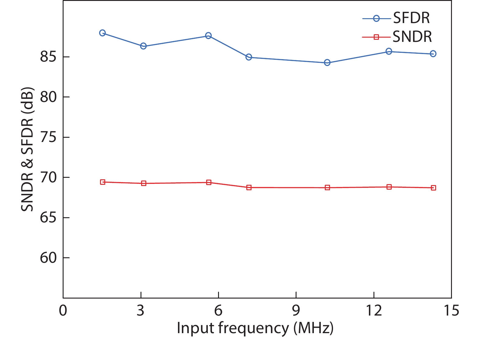
Abstract: This paper proposes a technique that uses the number of oscillation cycles (NOC) of a VCO-based comparator to set multiple adaptive bypass windows in a 12-bit successive approximation register (SAR) analog-to-digital converter (ADC). The analysis of the number of bit cycles, power and static performance shows that three adaptive bypass windows reduce power consumption, and decrease DNL and have similar INL, compared with the SAR ADC without bypass windows. In addition, a 1-bit split-and-recombination redundancy technique and a general bypass logic digital error correction method are proposed to address the settling issues and optimize the size of the bypass window. This design is implemented in 40 nm CMOS technology. The conversion frequency of the ADC reaches up to 30 MS/s. The ADC achieves an SFDR of 85.35 dB and 11.12-bit ENOB with Nyquist input, consuming 380 μW, down from 427 μW without multiple adaptive bypass windows, at a 1.1 V supply, resulting in a figure of merit (FoM) of 5.69 fJ/conversion-step.
Keywords: adaptive bypass window, number of oscillation cycles (NOC), offset, split-and-recombination redundancy, SAR ADC, VCO-based comparator
| [1] |
Zhu Y, Chan C, Chio U, et al. A 10-bit 100-MS/s reference-free SAR ADC in 90 nm CMOS. IEEE J Solid-State Circuits, 2010, 45(6), 1111 doi: 10.1109/JSSC.2010.2048498
|
| [2] |
Lin J, Hsieh C. A 0.3 V 10-bit 1.17 f SAR ADC with merge and split switching in 90 nm CMOS. IEEE Trans Circuits Syst I, 2015, 62(1), 70 doi: 10.1109/TCSI.2014.2349571
|
| [3] |
Sun L, Li B, Wong A K Y, et al. A charge recycling SAR ADC with a LSB-down switching scheme. IEEE Trans Circuits Syst I, 2015, 62(2), 356 doi: 10.1109/TCSI.2014.2363517
|
| [4] |
Lin J, Hsieh C. A 0.3 V 10-bit SAR ADC with first 2-bit guess in 90-nm CMOS. IEEE Trans Circuits Syst I, 2017, 64(3), 562 doi: 10.1109/TCSI.2016.2613505
|
| [5] |
Pang W, Wang C, Chang Y, et al. A 10-bit 500-kS/s low power SAR ADC with splitting comparator for bio-medical applications. 2009 IEEE Asian Solid-State Circuits Conference, 2009, 149
|
| [6] |
Zhu Z, Liang Y. A 0.6-V 38-nW 9.4-ENOB 20-kS/s SAR ADC in 0.18-μm CMOS for medical implant devices. IEEE Trans Circuits Syst I, 2015, 62(9), 2167 doi: 10.1109/TCSI.2015.2451812
|
| [7] |
Huang G, Chang S, Liu C, et al. A 1-μW 10-bit 200-kS/s SAR ADC with a bypass window for biomedical applications. IEEE J Solid-State Circuits, 2012, 47(11), 2783 doi: 10.1109/JSSC.2012.2217635
|
| [8] |
Nuzzo P, De Bernardinis F, Terreni P, et al. Noise analysis of regenerative comparators for reconfigurable ADC architectures. IEEE Trans Circuits Syst I, 2008, 55(6), 1441 doi: 10.1109/TCSI.2008.917991
|
| [9] |
Agnes A, Bonizzoni E, Malcovati P, et al. A 9.4-ENOB 1 V 3.8-µW 100 kS/s SAR ADC with time-domain comparator. 2008 IEEE International Solid-State Circuits Conference, 2018, 246
|
| [10] |
Lee S, Park S, Park H, et al. A 21 fJ/conversion-step 100 kS/s 10-bit ADC with a low-noise time-domain comparator for low-power sensor interface. IEEE J Solid-State Circuits, 2011, 46(3), 651 doi: 10.1109/JSSC.2010.2102590
|
| [11] |
Shim M, Jeong S, Myers P D, et al. Edge-pursuit comparator: An energy-scalable oscillator collapse-based comparator with application in a 74.1 dB SNDR and 20 kS/s 15 b SAR ADC. IEEE J Solid-State Circuits, 2017, 52(4), 1077 doi: 10.1109/JSSC.2016.2631299
|
| [12] |
Yoshioka K, Ishikuro H. A 13b SAR ADC with eye-opening VCO based comparator. ESSCIRC 2014: 40th European Solid State Circuits Conference (ESSCIRC), 2014, 411
|
| [13] |
Kao C, Hsieh S, Hsieh C. A 0.5 V 12-bit AR ADC using adaptive timedomain comparator with noise optimization. 2017 IEEE Asian Solid-State Circuits Conference (A-SSCC), 2017, 213
|
| [14] |
Harpe P, Cantatore E, van Roermund A. A 10b/12b 40 kS/s SAR ADC with data-driven noise reduction achieving up to 10.1b ENOB at 2.2 fJ/conversion-step. IEEE J Solid-State Circuits, 2013, 48(12), 3011 doi: 10.1109/JSSC.2013.2278471
|
| [15] |
Ahmadi M, Namgoong W. A 3.3fJ/conversion-step 250 kS/s 10b SAR ADC using optimized vote allocation. Proceedings of the IEEE 2013 Custom Integrated Circuits Conference, 2013, 1
|
| [16] |
Chen L, Tang X, Sanyal A, et al. A 0.7-V 0.6-μW 100-kS/s low-power SAR ADC with statistical estimation-based noise reduction. IEEE J Solid-State Circuits, 2017, 52(5), 1388 doi: 10.1109/JSSC.2017.2656138
|
| [17] |
Ding Z, Zhou X, Li Q. A 0.5–1.1-V adaptive bypassing SAR ADC utilizing the oscillation-cycle information of a VCO-based comparator. IEEE J Solid-State Circuits, 2019, 54(4), 968 doi: 10.1109/JSSC.2018.2885554
|
| [18] |
Chang S, Zhou X, Ding Z, et al. A 12-bit 30 MS/s SAR ADC with VCO-based comparator and split-and-recombination redundancy for bypass logic. 2019 IEEE International Symposium on Circuits and Systems (ISCAS), 2019, 1
|
| [19] |
Liu C, Kuo C, Lin Y. A 10 bit 320 MS/s low-cost SAR ADC for IEEE 802.11ac applications in 20 nm CMOS. IEEE J Solid-State Circuits, 2015, 50(11), 2645 doi: 10.1109/JSSC.2015.2466475
|
| [20] |
Abo A M, Gray P R. A 1.5 V, 10-bit, 14 MS/s CMOS pipeline analog-to-digital converter. 1998 Symposium on VLSI Circuits, 1998, 166
|
| [21] |
Kim J, Leibowitz B S, Ren J, et al. Simulation and analysis of random decision errors in clocked comparators. IEEE Trans Circuits Syst I, 2009, 56(8), 1844 doi: 10.1109/TCSI.2009.2028449
|
| [22] |
Abidi A A. Phase noise and jitter in CMOS ring oscillators. IEEE J Solid-State Circuits, 2006, 41(8), 1803 doi: 10.1109/JSSC.2006.876206
|
| [23] |
Tai H, Hu Y, Chen H, et al. 11.2 A 0.85fJ/conversion-step 10b 200 kS/s subranging SAR ADC in 40 nm CMOS. 2014 IEEE International Solid-State Circuits Conference, 2014, 196
|
| [24] |
Chen Y, Chang K, Hsieh C. A 2.02–5.16 fJ/conversion step 10 bit hybrid coarse-fine SAR ADC with time-domain quantizer in 90 nm CMOS. IEEE J Solid-State Circuits, 2016, 51(2), 357 doi: 10.1109/JSSC.2015.2492781
|
| [25] |
Chan C, Zhu Y, Ho I, et al. 16.4 a 5 mW 7b 2.4 GS/s 1-then-2b/cycle SAR ADC with background offset calibration. 2017 IEEE International Solid-State Circuits Conference (ISSCC), 2017, 282
|
| [26] |
Yoshioka K, Shikata A, Sekimoto R, et al. An 8 bit 0.35 –0.8 V 0.5–30 MS/s 2 bit/step SAR ADC with wide range threshold configuring comparator. 2012 Proceedings of the ESSCIRC (ESSCIRC), 2012, 381
|
| [27] |
Ragab K, Sun N. A 1.4 mW 8b 350 MS/s loop-unrolled SAR ADC with background offset calibration in 40 nm CMOS. ESSCIRC Conference 2016: 42nd European Solid-State Circuits Conference, 2016, 417
|
| [28] |
Chang A H, Lee H, Boning D. A 12b 50 MS/s 2.1 mw SAR ADC with redundancy and digital background calibration. 2013 Proceedings of the ESSCIRC (ESSCIRC), 2013, 109
|
| [29] |
Ginsburg B P, Chandrakasan A P. 500-MS/s 5-bit ADC in 65-nm CMOS with split capacitor array DAC. IEEE J Solid-State Circuits, 2007, 42(4), 739 doi: 10.1109/JSSC.2007.892169
|
| [30] |
Liu C, Chang S, Huang G, et al. A 10-bit 50-MS/s SAR ADC with a monotonic capacitor switching procedure. IEEE J Solid-State Circuits, 2010, 45(4), 731 doi: 10.1109/JSSC.2010.2042254
|
| [31] |
Wang T, Li H, Ma Z, et al. A bypass-switching SAR ADC with a dynamic proximity comparator for biomedical applications. IEEE J Solid-State Circuits, 2018, 53(6), 1743 doi: 10.1109/JSSC.2018.2819164
|
| [32] |
Liu C, Chang S, Huang G, et al. A 10b 100 MS/s 1.13 mW SAR ADC with binary-scaled error compensation. 2010 IEEE International Solid-State Circuits Conference (ISSCC), 2010, 386
|
| [33] |
Um J, Kim Y, Song E, et al. A digital-domain calibration of split-capacitor DAC for a differential SAR ADC without additional analog circuits. IEEE Trans Circuits Syst I, 2013, 60(11), 2845 doi: 10.1109/TCSI.2013.2252475
|
| [34] |
Jin J, Gao Y, Sánchez-Sinencio E. An energy-efficient time-domain asynchronous 2 b/step SAR ADC with a hybrid r-2r/c-3c DAC structure. IEEE J Solid-State Circuits, 2014, 49(6), 1383 doi: 10.1109/JSSC.2014.2317139
|

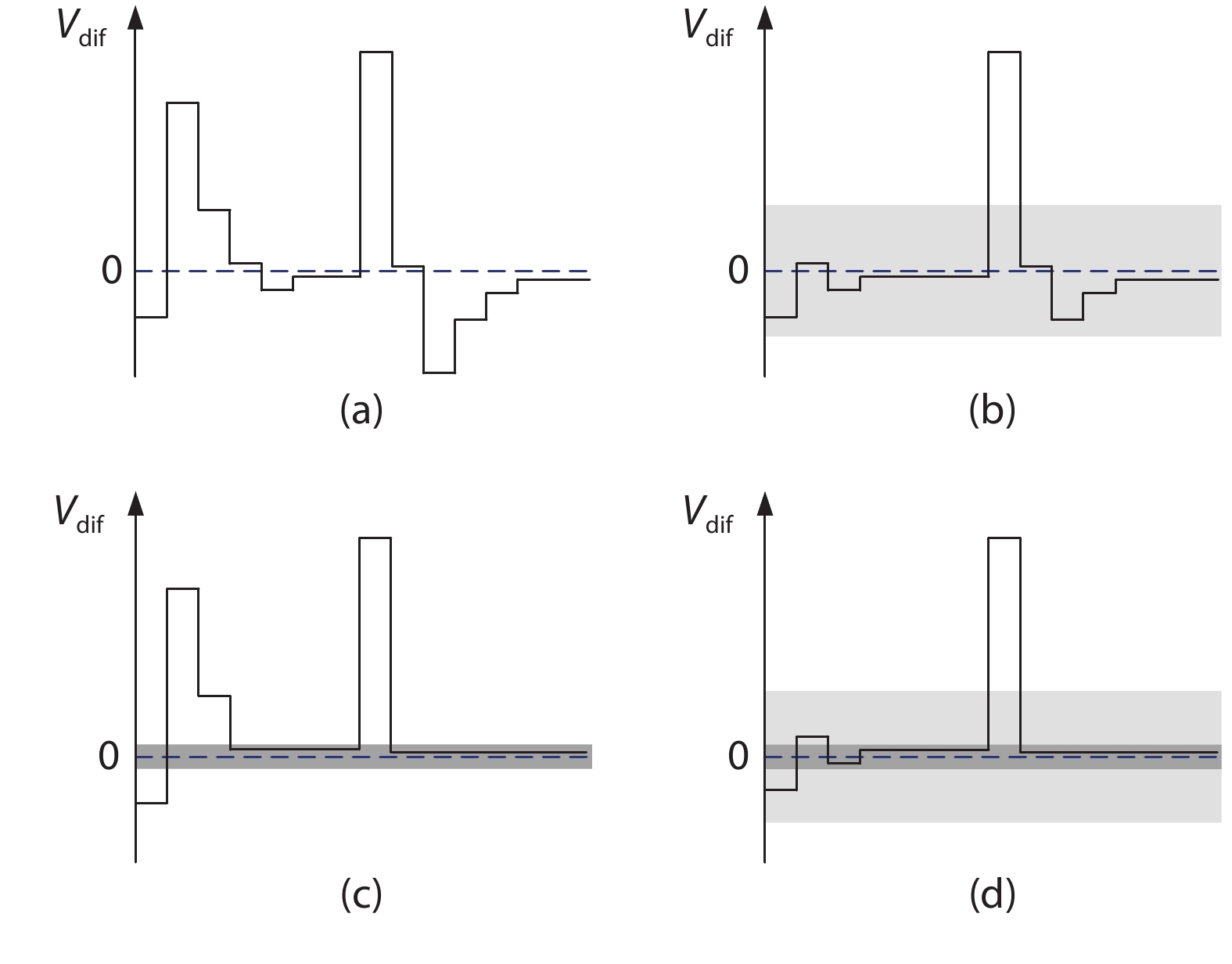


Table 1. Performance comparison of SAR ADCS with time-domain comparators.
| Parameter | JSSC 2011[10] | TCAS-I 2013[33] | JSSC 2014[34] | ESSCIRC 2014[12] | JSSC 2016[24] | JSSC 2017[11] | JSSC 2019[17] | This Work |
| Technology (nm) | 180 | 130 | 180 | 65 | 90 | 65 | 40 | 40 |
| Comparator type | VCDL | VCDL | VCDL hybrid | VCO | TDC hybrid | Edge-pursuit | VCO | VCO |
| Calibration | No | Yes | No | Yes | Yes | Yes | No | No |
| Supply voltage (V) | 0.6 | 0.5 | 0.6 | 0.85 | 0.7 | N/A | 1.1 | 1.1 |
| Conversion rate (MS/s) | 0.1 | 0.01 | 0.1 | 1.024 | 4 | 0.02 | 10 | 30 |
| Resolution (bit) | 10 | 11 | 10 | 13 | 10 | 15 | 10 | 12 |
| SFDR (dB) | 64 | 78 | 64.2 | 85.2 | 71.5 | 95.1 | 68.84 | 85.35 |
| SNDR (dB) | 57.5 | 61.6 | 56.5 | 66.4 | 54.8 | 74.12 | 58.57 | 68.72 |
| ENOB (bit) | 9.3 | 9.93 | 9.2 | 10.4 | 8.81 | 12.02 | 9.44 | 11.12 |
| Powe ( | 1.3 | 0.73 | 0.39 | 45.2 | 9.25 | 1.17 | 47.6 | 380 |
| FoM (fJ/Conv.-step) | 21 | 74.8 | 6.7 | 33 | 5.16 | 14.06 | 6.85 | 5.69 |
 DownLoad: CSV
| [1] |
Zhu Y, Chan C, Chio U, et al. A 10-bit 100-MS/s reference-free SAR ADC in 90 nm CMOS. IEEE J Solid-State Circuits, 2010, 45(6), 1111 doi: 10.1109/JSSC.2010.2048498
|
| [2] |
Lin J, Hsieh C. A 0.3 V 10-bit 1.17 f SAR ADC with merge and split switching in 90 nm CMOS. IEEE Trans Circuits Syst I, 2015, 62(1), 70 doi: 10.1109/TCSI.2014.2349571
|
| [3] |
Sun L, Li B, Wong A K Y, et al. A charge recycling SAR ADC with a LSB-down switching scheme. IEEE Trans Circuits Syst I, 2015, 62(2), 356 doi: 10.1109/TCSI.2014.2363517
|
| [4] |
Lin J, Hsieh C. A 0.3 V 10-bit SAR ADC with first 2-bit guess in 90-nm CMOS. IEEE Trans Circuits Syst I, 2017, 64(3), 562 doi: 10.1109/TCSI.2016.2613505
|
| [5] |
Pang W, Wang C, Chang Y, et al. A 10-bit 500-kS/s low power SAR ADC with splitting comparator for bio-medical applications. 2009 IEEE Asian Solid-State Circuits Conference, 2009, 149
|
| [6] |
Zhu Z, Liang Y. A 0.6-V 38-nW 9.4-ENOB 20-kS/s SAR ADC in 0.18-μm CMOS for medical implant devices. IEEE Trans Circuits Syst I, 2015, 62(9), 2167 doi: 10.1109/TCSI.2015.2451812
|
| [7] |
Huang G, Chang S, Liu C, et al. A 1-μW 10-bit 200-kS/s SAR ADC with a bypass window for biomedical applications. IEEE J Solid-State Circuits, 2012, 47(11), 2783 doi: 10.1109/JSSC.2012.2217635
|
| [8] |
Nuzzo P, De Bernardinis F, Terreni P, et al. Noise analysis of regenerative comparators for reconfigurable ADC architectures. IEEE Trans Circuits Syst I, 2008, 55(6), 1441 doi: 10.1109/TCSI.2008.917991
|
| [9] |
Agnes A, Bonizzoni E, Malcovati P, et al. A 9.4-ENOB 1 V 3.8-µW 100 kS/s SAR ADC with time-domain comparator. 2008 IEEE International Solid-State Circuits Conference, 2018, 246
|
| [10] |
Lee S, Park S, Park H, et al. A 21 fJ/conversion-step 100 kS/s 10-bit ADC with a low-noise time-domain comparator for low-power sensor interface. IEEE J Solid-State Circuits, 2011, 46(3), 651 doi: 10.1109/JSSC.2010.2102590
|
| [11] |
Shim M, Jeong S, Myers P D, et al. Edge-pursuit comparator: An energy-scalable oscillator collapse-based comparator with application in a 74.1 dB SNDR and 20 kS/s 15 b SAR ADC. IEEE J Solid-State Circuits, 2017, 52(4), 1077 doi: 10.1109/JSSC.2016.2631299
|
| [12] |
Yoshioka K, Ishikuro H. A 13b SAR ADC with eye-opening VCO based comparator. ESSCIRC 2014: 40th European Solid State Circuits Conference (ESSCIRC), 2014, 411
|
| [13] |
Kao C, Hsieh S, Hsieh C. A 0.5 V 12-bit AR ADC using adaptive timedomain comparator with noise optimization. 2017 IEEE Asian Solid-State Circuits Conference (A-SSCC), 2017, 213
|
| [14] |
Harpe P, Cantatore E, van Roermund A. A 10b/12b 40 kS/s SAR ADC with data-driven noise reduction achieving up to 10.1b ENOB at 2.2 fJ/conversion-step. IEEE J Solid-State Circuits, 2013, 48(12), 3011 doi: 10.1109/JSSC.2013.2278471
|
| [15] |
Ahmadi M, Namgoong W. A 3.3fJ/conversion-step 250 kS/s 10b SAR ADC using optimized vote allocation. Proceedings of the IEEE 2013 Custom Integrated Circuits Conference, 2013, 1
|
| [16] |
Chen L, Tang X, Sanyal A, et al. A 0.7-V 0.6-μW 100-kS/s low-power SAR ADC with statistical estimation-based noise reduction. IEEE J Solid-State Circuits, 2017, 52(5), 1388 doi: 10.1109/JSSC.2017.2656138
|
| [17] |
Ding Z, Zhou X, Li Q. A 0.5–1.1-V adaptive bypassing SAR ADC utilizing the oscillation-cycle information of a VCO-based comparator. IEEE J Solid-State Circuits, 2019, 54(4), 968 doi: 10.1109/JSSC.2018.2885554
|
| [18] |
Chang S, Zhou X, Ding Z, et al. A 12-bit 30 MS/s SAR ADC with VCO-based comparator and split-and-recombination redundancy for bypass logic. 2019 IEEE International Symposium on Circuits and Systems (ISCAS), 2019, 1
|
| [19] |
Liu C, Kuo C, Lin Y. A 10 bit 320 MS/s low-cost SAR ADC for IEEE 802.11ac applications in 20 nm CMOS. IEEE J Solid-State Circuits, 2015, 50(11), 2645 doi: 10.1109/JSSC.2015.2466475
|
| [20] |
Abo A M, Gray P R. A 1.5 V, 10-bit, 14 MS/s CMOS pipeline analog-to-digital converter. 1998 Symposium on VLSI Circuits, 1998, 166
|
| [21] |
Kim J, Leibowitz B S, Ren J, et al. Simulation and analysis of random decision errors in clocked comparators. IEEE Trans Circuits Syst I, 2009, 56(8), 1844 doi: 10.1109/TCSI.2009.2028449
|
| [22] |
Abidi A A. Phase noise and jitter in CMOS ring oscillators. IEEE J Solid-State Circuits, 2006, 41(8), 1803 doi: 10.1109/JSSC.2006.876206
|
| [23] |
Tai H, Hu Y, Chen H, et al. 11.2 A 0.85fJ/conversion-step 10b 200 kS/s subranging SAR ADC in 40 nm CMOS. 2014 IEEE International Solid-State Circuits Conference, 2014, 196
|
| [24] |
Chen Y, Chang K, Hsieh C. A 2.02–5.16 fJ/conversion step 10 bit hybrid coarse-fine SAR ADC with time-domain quantizer in 90 nm CMOS. IEEE J Solid-State Circuits, 2016, 51(2), 357 doi: 10.1109/JSSC.2015.2492781
|
| [25] |
Chan C, Zhu Y, Ho I, et al. 16.4 a 5 mW 7b 2.4 GS/s 1-then-2b/cycle SAR ADC with background offset calibration. 2017 IEEE International Solid-State Circuits Conference (ISSCC), 2017, 282
|
| [26] |
Yoshioka K, Shikata A, Sekimoto R, et al. An 8 bit 0.35 –0.8 V 0.5–30 MS/s 2 bit/step SAR ADC with wide range threshold configuring comparator. 2012 Proceedings of the ESSCIRC (ESSCIRC), 2012, 381
|
| [27] |
Ragab K, Sun N. A 1.4 mW 8b 350 MS/s loop-unrolled SAR ADC with background offset calibration in 40 nm CMOS. ESSCIRC Conference 2016: 42nd European Solid-State Circuits Conference, 2016, 417
|
| [28] |
Chang A H, Lee H, Boning D. A 12b 50 MS/s 2.1 mw SAR ADC with redundancy and digital background calibration. 2013 Proceedings of the ESSCIRC (ESSCIRC), 2013, 109
|
| [29] |
Ginsburg B P, Chandrakasan A P. 500-MS/s 5-bit ADC in 65-nm CMOS with split capacitor array DAC. IEEE J Solid-State Circuits, 2007, 42(4), 739 doi: 10.1109/JSSC.2007.892169
|
| [30] |
Liu C, Chang S, Huang G, et al. A 10-bit 50-MS/s SAR ADC with a monotonic capacitor switching procedure. IEEE J Solid-State Circuits, 2010, 45(4), 731 doi: 10.1109/JSSC.2010.2042254
|
| [31] |
Wang T, Li H, Ma Z, et al. A bypass-switching SAR ADC with a dynamic proximity comparator for biomedical applications. IEEE J Solid-State Circuits, 2018, 53(6), 1743 doi: 10.1109/JSSC.2018.2819164
|
| [32] |
Liu C, Chang S, Huang G, et al. A 10b 100 MS/s 1.13 mW SAR ADC with binary-scaled error compensation. 2010 IEEE International Solid-State Circuits Conference (ISSCC), 2010, 386
|
| [33] |
Um J, Kim Y, Song E, et al. A digital-domain calibration of split-capacitor DAC for a differential SAR ADC without additional analog circuits. IEEE Trans Circuits Syst I, 2013, 60(11), 2845 doi: 10.1109/TCSI.2013.2252475
|
| [34] |
Jin J, Gao Y, Sánchez-Sinencio E. An energy-efficient time-domain asynchronous 2 b/step SAR ADC with a hybrid r-2r/c-3c DAC structure. IEEE J Solid-State Circuits, 2014, 49(6), 1383 doi: 10.1109/JSSC.2014.2317139
|


Article views: 6851 Times PDF downloads: 188 Times Cited by: 0 Times
Received: 22 June 2020 Revised: 15 July 2020 Online: Accepted Manuscript: 18 September 2020Uncorrected proof: 24 September 2020Published: 03 November 2020
| Citation: |
Xiangxin Pan, Xiong Zhou, Sheng Chang, Zhaoming Ding, Qiang Li. A 12-bit 30-MS/s VCO-based SAR ADC with NOC-assisted multiple adaptive bypass windows[J]. Journal of Semiconductors, 2020, 41(11): 112401. doi: 10.1088/1674-4926/41/11/112401
****
X X Pan, X Zhou, S Chang, Z M Ding, Q Li, A 12-bit 30-MS/s VCO-based SAR ADC with NOC-assisted multiple adaptive bypass windows[J]. J. Semicond., 2020, 41(11): 112401. doi: 10.1088/1674-4926/41/11/112401.

|
| [1] |
Zhu Y, Chan C, Chio U, et al. A 10-bit 100-MS/s reference-free SAR ADC in 90 nm CMOS. IEEE J Solid-State Circuits, 2010, 45(6), 1111 doi: 10.1109/JSSC.2010.2048498
|
| [2] |
Lin J, Hsieh C. A 0.3 V 10-bit 1.17 f SAR ADC with merge and split switching in 90 nm CMOS. IEEE Trans Circuits Syst I, 2015, 62(1), 70 doi: 10.1109/TCSI.2014.2349571
|
| [3] |
Sun L, Li B, Wong A K Y, et al. A charge recycling SAR ADC with a LSB-down switching scheme. IEEE Trans Circuits Syst I, 2015, 62(2), 356 doi: 10.1109/TCSI.2014.2363517
|
| [4] |
Lin J, Hsieh C. A 0.3 V 10-bit SAR ADC with first 2-bit guess in 90-nm CMOS. IEEE Trans Circuits Syst I, 2017, 64(3), 562 doi: 10.1109/TCSI.2016.2613505
|
| [5] |
Pang W, Wang C, Chang Y, et al. A 10-bit 500-kS/s low power SAR ADC with splitting comparator for bio-medical applications. 2009 IEEE Asian Solid-State Circuits Conference, 2009, 149
|
| [6] |
Zhu Z, Liang Y. A 0.6-V 38-nW 9.4-ENOB 20-kS/s SAR ADC in 0.18-μm CMOS for medical implant devices. IEEE Trans Circuits Syst I, 2015, 62(9), 2167 doi: 10.1109/TCSI.2015.2451812
|
| [7] |
Huang G, Chang S, Liu C, et al. A 1-μW 10-bit 200-kS/s SAR ADC with a bypass window for biomedical applications. IEEE J Solid-State Circuits, 2012, 47(11), 2783 doi: 10.1109/JSSC.2012.2217635
|
| [8] |
Nuzzo P, De Bernardinis F, Terreni P, et al. Noise analysis of regenerative comparators for reconfigurable ADC architectures. IEEE Trans Circuits Syst I, 2008, 55(6), 1441 doi: 10.1109/TCSI.2008.917991
|
| [9] |
Agnes A, Bonizzoni E, Malcovati P, et al. A 9.4-ENOB 1 V 3.8-µW 100 kS/s SAR ADC with time-domain comparator. 2008 IEEE International Solid-State Circuits Conference, 2018, 246
|
| [10] |
Lee S, Park S, Park H, et al. A 21 fJ/conversion-step 100 kS/s 10-bit ADC with a low-noise time-domain comparator for low-power sensor interface. IEEE J Solid-State Circuits, 2011, 46(3), 651 doi: 10.1109/JSSC.2010.2102590
|
| [11] |
Shim M, Jeong S, Myers P D, et al. Edge-pursuit comparator: An energy-scalable oscillator collapse-based comparator with application in a 74.1 dB SNDR and 20 kS/s 15 b SAR ADC. IEEE J Solid-State Circuits, 2017, 52(4), 1077 doi: 10.1109/JSSC.2016.2631299
|
| [12] |
Yoshioka K, Ishikuro H. A 13b SAR ADC with eye-opening VCO based comparator. ESSCIRC 2014: 40th European Solid State Circuits Conference (ESSCIRC), 2014, 411
|
| [13] |
Kao C, Hsieh S, Hsieh C. A 0.5 V 12-bit AR ADC using adaptive timedomain comparator with noise optimization. 2017 IEEE Asian Solid-State Circuits Conference (A-SSCC), 2017, 213
|
| [14] |
Harpe P, Cantatore E, van Roermund A. A 10b/12b 40 kS/s SAR ADC with data-driven noise reduction achieving up to 10.1b ENOB at 2.2 fJ/conversion-step. IEEE J Solid-State Circuits, 2013, 48(12), 3011 doi: 10.1109/JSSC.2013.2278471
|
| [15] |
Ahmadi M, Namgoong W. A 3.3fJ/conversion-step 250 kS/s 10b SAR ADC using optimized vote allocation. Proceedings of the IEEE 2013 Custom Integrated Circuits Conference, 2013, 1
|
| [16] |
Chen L, Tang X, Sanyal A, et al. A 0.7-V 0.6-μW 100-kS/s low-power SAR ADC with statistical estimation-based noise reduction. IEEE J Solid-State Circuits, 2017, 52(5), 1388 doi: 10.1109/JSSC.2017.2656138
|
| [17] |
Ding Z, Zhou X, Li Q. A 0.5–1.1-V adaptive bypassing SAR ADC utilizing the oscillation-cycle information of a VCO-based comparator. IEEE J Solid-State Circuits, 2019, 54(4), 968 doi: 10.1109/JSSC.2018.2885554
|
| [18] |
Chang S, Zhou X, Ding Z, et al. A 12-bit 30 MS/s SAR ADC with VCO-based comparator and split-and-recombination redundancy for bypass logic. 2019 IEEE International Symposium on Circuits and Systems (ISCAS), 2019, 1
|
| [19] |
Liu C, Kuo C, Lin Y. A 10 bit 320 MS/s low-cost SAR ADC for IEEE 802.11ac applications in 20 nm CMOS. IEEE J Solid-State Circuits, 2015, 50(11), 2645 doi: 10.1109/JSSC.2015.2466475
|
| [20] |
Abo A M, Gray P R. A 1.5 V, 10-bit, 14 MS/s CMOS pipeline analog-to-digital converter. 1998 Symposium on VLSI Circuits, 1998, 166
|
| [21] |
Kim J, Leibowitz B S, Ren J, et al. Simulation and analysis of random decision errors in clocked comparators. IEEE Trans Circuits Syst I, 2009, 56(8), 1844 doi: 10.1109/TCSI.2009.2028449
|
| [22] |
Abidi A A. Phase noise and jitter in CMOS ring oscillators. IEEE J Solid-State Circuits, 2006, 41(8), 1803 doi: 10.1109/JSSC.2006.876206
|
| [23] |
Tai H, Hu Y, Chen H, et al. 11.2 A 0.85fJ/conversion-step 10b 200 kS/s subranging SAR ADC in 40 nm CMOS. 2014 IEEE International Solid-State Circuits Conference, 2014, 196
|
| [24] |
Chen Y, Chang K, Hsieh C. A 2.02–5.16 fJ/conversion step 10 bit hybrid coarse-fine SAR ADC with time-domain quantizer in 90 nm CMOS. IEEE J Solid-State Circuits, 2016, 51(2), 357 doi: 10.1109/JSSC.2015.2492781
|
| [25] |
Chan C, Zhu Y, Ho I, et al. 16.4 a 5 mW 7b 2.4 GS/s 1-then-2b/cycle SAR ADC with background offset calibration. 2017 IEEE International Solid-State Circuits Conference (ISSCC), 2017, 282
|
| [26] |
Yoshioka K, Shikata A, Sekimoto R, et al. An 8 bit 0.35 –0.8 V 0.5–30 MS/s 2 bit/step SAR ADC with wide range threshold configuring comparator. 2012 Proceedings of the ESSCIRC (ESSCIRC), 2012, 381
|
| [27] |
Ragab K, Sun N. A 1.4 mW 8b 350 MS/s loop-unrolled SAR ADC with background offset calibration in 40 nm CMOS. ESSCIRC Conference 2016: 42nd European Solid-State Circuits Conference, 2016, 417
|
| [28] |
Chang A H, Lee H, Boning D. A 12b 50 MS/s 2.1 mw SAR ADC with redundancy and digital background calibration. 2013 Proceedings of the ESSCIRC (ESSCIRC), 2013, 109
|
| [29] |
Ginsburg B P, Chandrakasan A P. 500-MS/s 5-bit ADC in 65-nm CMOS with split capacitor array DAC. IEEE J Solid-State Circuits, 2007, 42(4), 739 doi: 10.1109/JSSC.2007.892169
|
| [30] |
Liu C, Chang S, Huang G, et al. A 10-bit 50-MS/s SAR ADC with a monotonic capacitor switching procedure. IEEE J Solid-State Circuits, 2010, 45(4), 731 doi: 10.1109/JSSC.2010.2042254
|
| [31] |
Wang T, Li H, Ma Z, et al. A bypass-switching SAR ADC with a dynamic proximity comparator for biomedical applications. IEEE J Solid-State Circuits, 2018, 53(6), 1743 doi: 10.1109/JSSC.2018.2819164
|
| [32] |
Liu C, Chang S, Huang G, et al. A 10b 100 MS/s 1.13 mW SAR ADC with binary-scaled error compensation. 2010 IEEE International Solid-State Circuits Conference (ISSCC), 2010, 386
|
| [33] |
Um J, Kim Y, Song E, et al. A digital-domain calibration of split-capacitor DAC for a differential SAR ADC without additional analog circuits. IEEE Trans Circuits Syst I, 2013, 60(11), 2845 doi: 10.1109/TCSI.2013.2252475
|
| [34] |
Jin J, Gao Y, Sánchez-Sinencio E. An energy-efficient time-domain asynchronous 2 b/step SAR ADC with a hybrid r-2r/c-3c DAC structure. IEEE J Solid-State Circuits, 2014, 49(6), 1383 doi: 10.1109/JSSC.2014.2317139
|

 WeChat ID
Journal of Semiconductors © 2017 All Rights Reserved 京ICP备05085259号-2