


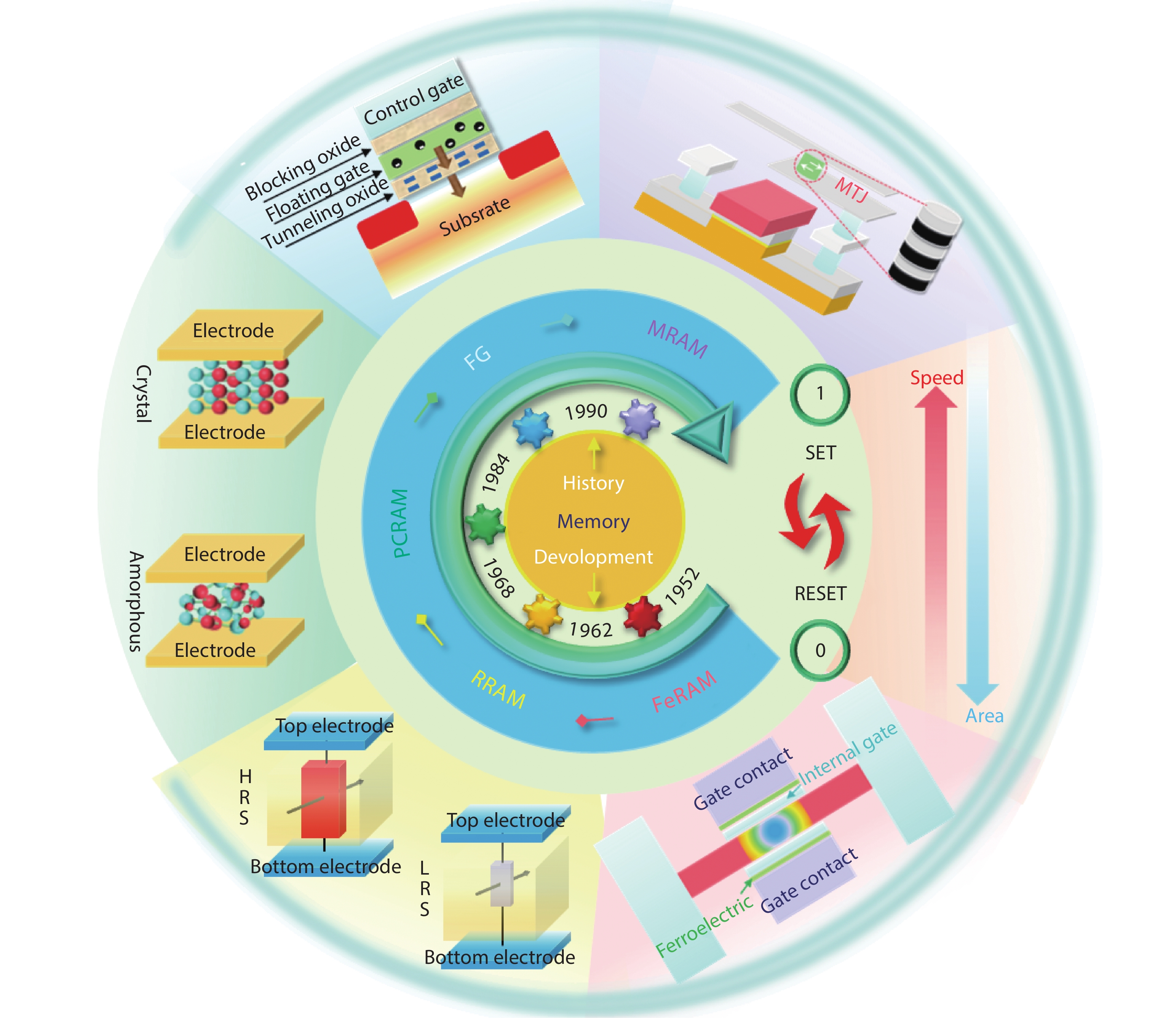
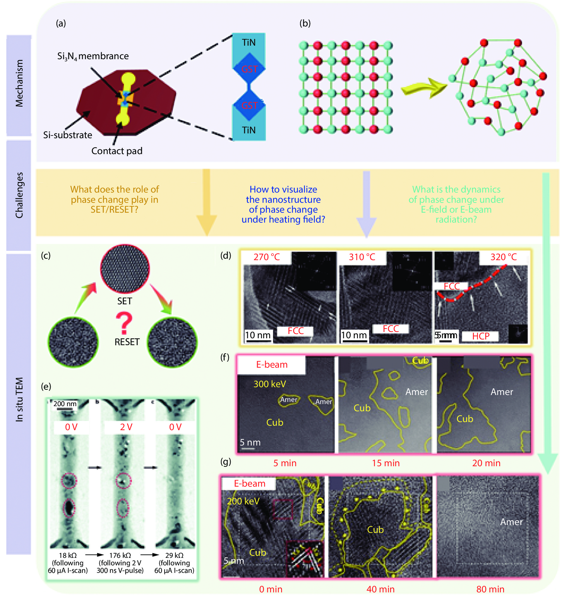
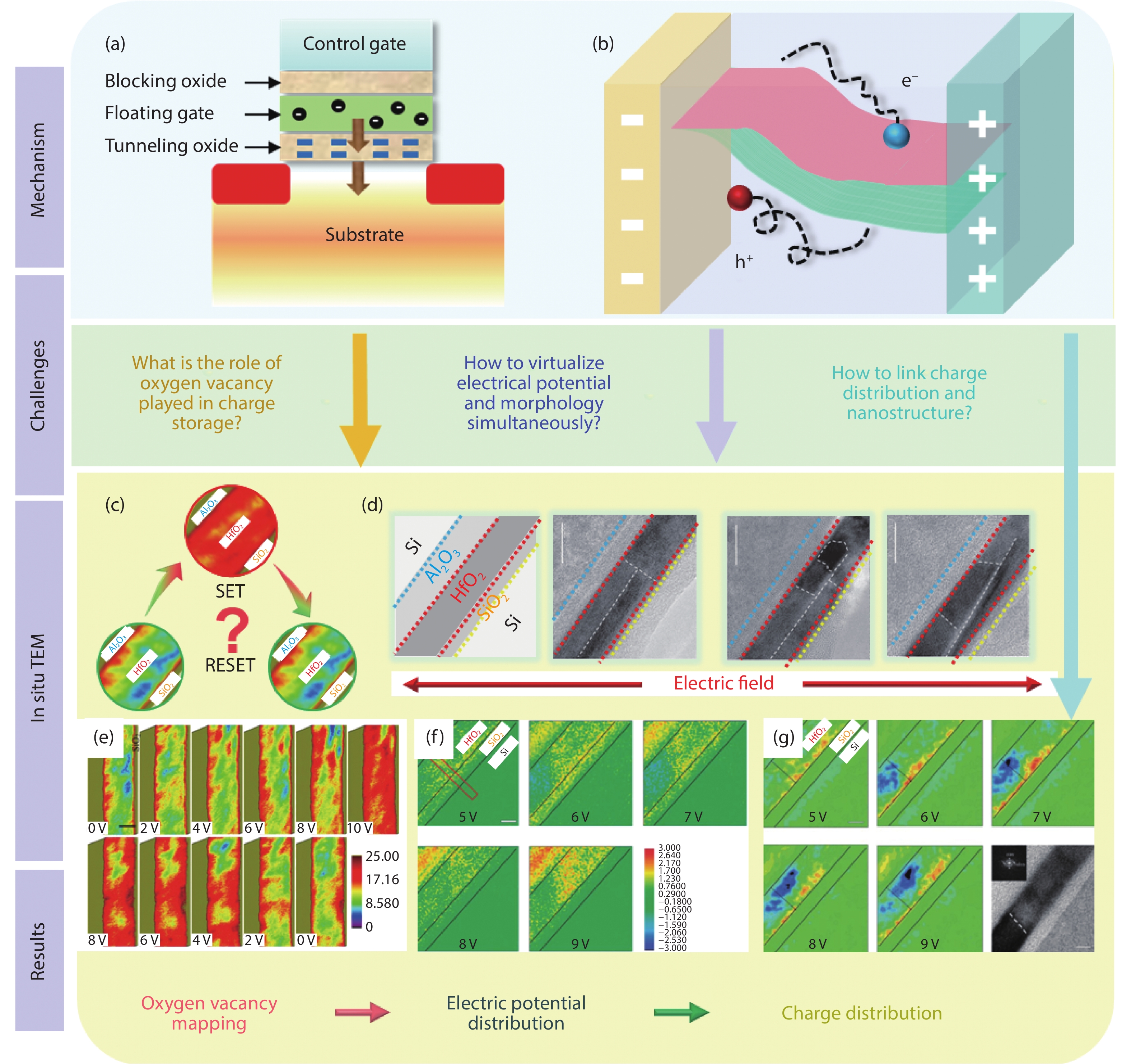
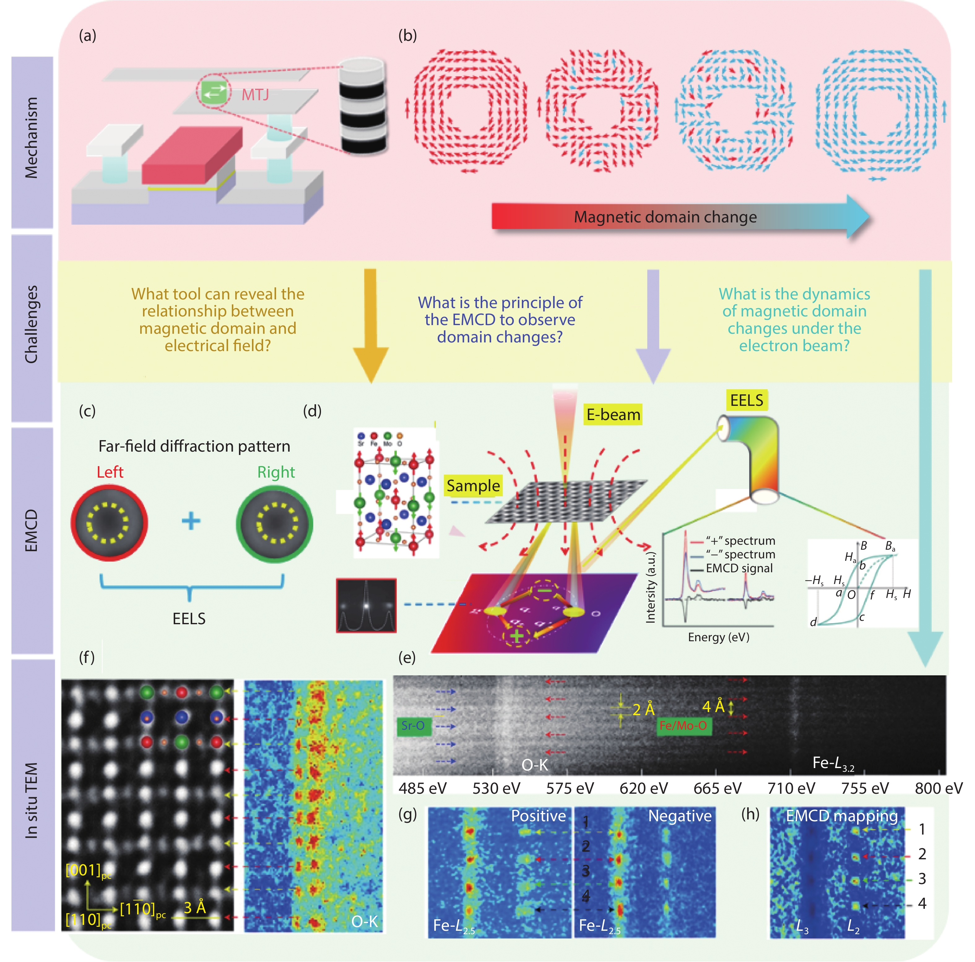
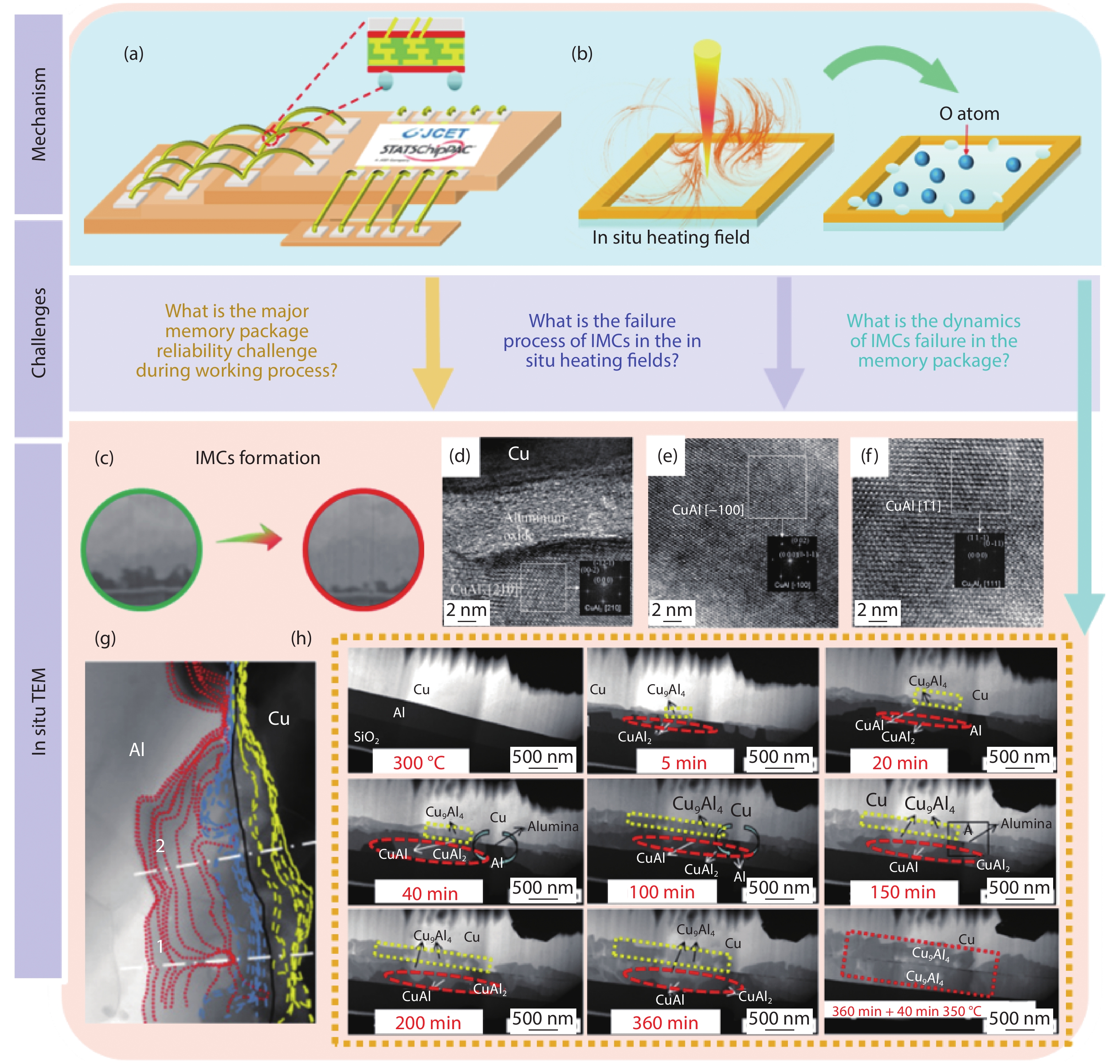
Fig. 1.
(Color online) Advanced non-volatile memory devices.
REVIEWS
Xin Yang1, Chen Luo1, Xiyue Tian1, Fang Liang1, Yin Xia1, Xinqian Chen1, Chaolun Wang1, Steve Xin Liang2, Xing Wu1, and Junhao Chu1
Corresponding author: Xing Wu, Email: xwu@cee.ecnu.edu.cn
Abstract: Non-volatile memory (NVM) devices with non-volatility and low power consumption properties are important in the data storage field. The switching mechanism and packaging reliability issues in NVMs are of great research interest. The switching process in NVM devices accompanied by the evolution of microstructure and composition is fast and subtle. Transmission electron microscopy (TEM) with high spatial resolution and versatile external fields is widely used in analyzing the evolution of morphology, structures and chemical compositions at atomic scale. The various external stimuli, such as thermal, electrical, mechanical, optical and magnetic fields, provide a platform to probe and engineer NVM devices inside TEM in real-time. Such advanced technologies make it possible for an in situ and interactive manipulation of NVM devices without sacrificing the resolution. This technology facilitates the exploration of the intrinsic structure-switching mechanism of NVMs and the reliability issues in the memory package. In this review, the evolution of the functional layers in NVM devices characterized by the advanced in situ TEM technology is introduced, with intermetallic compounds forming and degradation process investigated. The principles and challenges of TEM technology on NVM device study are also discussed.
Keywords: memory, transmission electron microscopy, in situ characterization, package, reliability
| [1] |
Luo C, Wang C L, Wu X, et al. In situ transmission electron microscopy characterization and manipulation of two-dimensional layered materials beyond graphene. Small, 2017, 13, 1604259 doi: 10.1002/smll.201604259
|
| [2] |
Jiang Y, Chen Z, Han Y M, et al. Electron ptychography of 2D materials to deep sub-ångström resolution. Nature, 2018, 559, 343 doi: 10.1038/s41586-018-0298-5
|
| [3] |
Xu H, Wu X, Tian X, et al. Dynamic structure-properties characterization and manipulation in advanced nanodevices. Mater Today Nano, 2019, 7, 100042 doi: 10.1016/j.mtnano.2019.100042
|
| [4] |
Lanza M, Wong H S P, Pop E, et al. Recommended methods to study resistive switching devices. Adv Electron Mater, 2019, 5, 1800143 doi: 10.1002/aelm.201800143
|
| [5] |
Fan Z, Zhang L Q, Baumann D, et al. In situ transmission electron microscopy for energy materials and devices. Adv Mater, 2019, 31, 1900608 doi: 10.1002/adma.201900608
|
| [6] |
Cao Y M, Zhang B, Tian X Y, et al. Direct covalent modification of black phosphorus quantum dots with conjugated polymers for information storage. Nanoscale, 2019, 11, 3527 doi: 10.1039/C8NR09711A
|
| [7] |
Endoh T, Koike H, Ikeda S, et al. An overview of nonvolatile emerging memories: Spintronics for working memories. IEEE J Emerg Sel Top Circuits Syst, 2016, 6, 109 doi: 10.1109/JETCAS.2016.2547704
|
| [8] |
Zhang Z H, Wang Z W, Shi T, et al. Memory materials and devices: From concept to application. InfoMat, 2020, 2, 261 doi: 10.1002/inf2.12077
|
| [9] |
Sun W, Gao B, Chi M F, et al. Understanding memristive switching via in situ characterization and device modeling. Nat Commun, 2019, 10, 3453 doi: 10.1038/s41467-019-11411-6
|
| [10] |
Lee S H, Zhu X J, Lu W D. Nanoscale resistive switching devices for memory and computing applications. Nano Res, 2020, 13, 1228 doi: 10.1007/s12274-020-2616-0
|
| [11] |
Zhang Y, Wang Z R, Zhu J D, et al. Brain-inspired computing with memristors: Challenges in devices, circuits, and systems. Appl Phys Rev, 2020, 7, 011308 doi: 10.1063/1.5124027
|
| [12] |
Wang Z P, Zhang S R, Zhou L, et al. Functional non-volatile memory devices: From fundamentals to photo-tunable properties. Phys Status Solidi RRL, 2019, 13, 1970022 doi: 10.1002/pssr.201800644
|
| [13] |
Younis A, Li S A. Microscopic investigations of switching phenomenon in memristive systems: A mini review. RSC Adv, 2018, 8, 28763 doi: 10.1039/C8RA05340E
|
| [14] |
Gao H, Yang Y X, Wang Y J, et al. Transparent, flexible, fatigue-free, optical-read, and nonvolatile ferroelectric memories. ACS Appl Mater Interfaces, 2019, 11, 35169 doi: 10.1021/acsami.9b14095
|
| [15] |
Si M W, Saha A K, Gao S J, et al. A ferroelectric semiconductor field-effect transistor. Nat Electron, 2019, 2, 580 doi: 10.1038/s41928-019-0338-7
|
| [16] |
Cao R R, Liu Q, Liu M, et al. Improvement of endurance in HZO-based ferroelectric capacitor using Ru electrode. IEEE Electron Device Lett, 2019, 40, 1744 doi: 10.1109/LED.2019.2944960
|
| [17] |
Chang T C, Chang K C, Tsai T M, et al. Resistance random access memory. Mater Today, 2016, 19, 254 doi: 10.1016/j.mattod.2015.11.009
|
| [18] |
Wang H, Yan X B. Overview of resistive random access memory (RRAM): Materials, filament mechanisms, performance optimization, and prospects. Phys Status Solidi RRL, 2019, 13, 1900073 doi: 10.1002/pssr.201900073
|
| [19] |
Yen T J, Gismatulin A, Volodin V, et al. All nonmetal resistive random access memory. Sci Rep, 2019, 9, 6144 doi: 10.1038/s41598-019-42706-9
|
| [20] |
Li W Q, Zhan X Y, Song X Y, et al. A review of recent applications of ion beam techniques on nanomaterial surface modification: Design of nanostructures and energy harvesting. Small, 2019, 15, 1901820 doi: 10.1002/smll.201901820
|
| [21] |
Zhang W, Mazzarello R, Wuttig M, et al. Designing crystallization in phase-change materials for universal memory and neuro-inspired computing. Nat Rev Mater, 2019, 4, 150 doi: 10.1038/s41578-018-0076-x
|
| [22] |
Burr G W, Brightsky M J, Sebastian A, et al. Recent progress in phase-change_newline memory technology. IEEE J Emerg Sel Top Circuits Syst, 2016, 6, 146 doi: 10.1109/JETCAS.2016.2547718
|
| [23] |
Jiang T T, Wang J J, Lu L, et al. Progressive amorphization of GeSbTe phase-change material under electron beam irradiation. APL Mater, 2019, 7, 081121 doi: 10.1063/1.5102075
|
| [24] |
Wang P F, Lin X, Liu L, et al. A semi-floating gate transistor for low-voltage ultrafast memory and sensing operation. Science, 2013, 341, 640 doi: 10.1126/science.1240961
|
| [25] |
Yao Y, Liu L, Ye Z Y, et al. Investigation of device physics and modeling of semi-floating gate image sensor cell. Microelectron Eng, 2019, 217, 111111 doi: 10.1016/j.mee.2019.111111
|
| [26] |
Rathore J S, Fandan R, Srivastava S, et al. Self-assembled Sn nanocrystals as the floating gate of nonvolatile flash memory. ACS Appl Electron Mater, 2019, 1, 1852 doi: 10.1021/acsaelm.9b00379
|
| [27] |
Yao Y, Li C, Huo Z L, et al. In situ electron holography study of charge distribution in high-κ charge-trapping memory. Nat Commun, 2013, 4, 2764 doi: 10.1038/ncomms3764
|
| [28] |
Fernández-Pacheco A, Streubel R, Fruchart O, et al. Three-dimensional nanomagnetism. Nat Commun, 2017, 8, 15756 doi: 10.1038/ncomms15756
|
| [29] |
Yakushiji K, Sugihara A, Nakano T, et al. Fully epitaxial magnetic tunnel junction on a silicon wafer. Appl Phys Lett, 2019, 115, 202403 doi: 10.1063/1.5116055
|
| [30] |
Stavrou V D, Kourounis D, Dimakopoulos K, et al. Magnetic skyrmions in FePt nanoparticles having Reuleaux 3D geometry: A micromagnetic simulation study. Nanoscale, 2019, 11, 20102 doi: 10.1039/C9NR04829D
|
| [31] |
Yang Z, Mi X J, Feng X, et al. Interface evolution of Cu–Ni–Si/Al–Mg–Si clad composite wires after annealing. Rare Met, 2018, 42, 1 doi: 10.1007/s12598-018-1073-3
|
| [32] |
Moisy F, Sauvage X, Hug E. Investigation of the early stage of reactive interdiffusion in the Cu-Al system by in situ transmission electron microscopy. Materialia, 2020, 9, 100633 doi: 10.1016/j.mtla.2020.100633
|
| [33] |
Xu H, Liu C, Silberschmidt V V, et al. Behavior of aluminum oxide, intermetallics and voids in Cu–Al wire bonds. Acta Mater, 2011, 59, 5661 doi: 10.1016/j.actamat.2011.05.041
|
| [34] |
Liu C P, Chang S J, Liu Y F, et al. Cu–Al interfacial formation and kinetic growth behavior during HTS reliability test. J Mater Process Technol, 2019, 267, 90 doi: 10.1016/j.jmatprotec.2018.12.012
|
| [35] |
Liu D, Chen H B, Wu J S, et al. Corrosion behavior of Cu–Al intermetallic compounds in copper wire bonding in chloride-containing accelerated humidity testing. 2016 IEEE 66th Electronic Components and Technology Conference (ECTC), 2016, 629
|
| [36] |
Xu H, Qin I, Clauberg H, et al. New observation of nanoscale interfacial evolution in micro Cu–Al wire bonds by in situ high resolution TEM study. Scr Mater, 2016, 115, 1 doi: 10.1016/j.scriptamat.2015.12.025
|
| [37] |
Tan Y Y, Yang Q L, Sim K S, et al. Cu–Al intermetallic compound investigation using ex-situ post annealing and in situ annealing. Microelectron Reliab, 2015, 55, 2316 doi: 10.1016/j.microrel.2015.06.050
|
| [38] |
Wang C M. In situ transmission electron microscopy and spectroscopy studies of rechargeable batteries under dynamic operating conditions: A retrospective and perspective view. J Mater Res, 2015, 30, 326 doi: 10.1557/jmr.2014.281
|
| [39] |
Legros M. In situ mechanical TEM: Seeing and measuring under stress with electrons. Comptes Rendus Physique, 2014, 15, 224 doi: 10.1016/j.crhy.2014.02.002
|
| [40] |
Xiang B, Hwang D J, In J B, et al. In situ TEM near-field optical probing of nanoscale silicon crystallization. Nano Lett, 2012, 12, 2524 doi: 10.1021/nl3007352
|
| [41] |
Evans J E, Jungjohann K L, Browning N D, et al. Controlled growth of nanoparticles from solution with in situ liquid transmission electron microscopy. Nano Lett, 2011, 11, 2809 doi: 10.1021/nl201166k
|
| [42] |
Chernavskii P A, Pankina G V, Chernavskii A P, et al. In situ magnetic study of the low-temperature oxidation of carbon-supported cobalt nanoparticles. J Phys Chem C, 2007, 111, 5576 doi: 10.1021/jp065162h
|
| [43] |
Midgley P A, Dunin-Borkowski R E. Electron tomography and holography in materials science. Nat Mater, 2009, 8, 271 doi: 10.1038/nmat2406
|
| [44] |
Zweck J. Imaging of magnetic and electric fields by electron microscopy. J Phys: Condens Matter, 2016, 28, 403001 doi: 10.1088/0953-8984/28/40/403001
|
| [45] |
Yang H, Li Y L, Zhu H L, et al. Advanced TEM application in 10nm below technology node device analysis. 2019 IEEE 26th International Symposium on Physical and Failure Analysis of Integrated Circuits (IPFA), 2019, 1
|
| [46] |
Choi S J, Park G S, Kim K H, et al. In situ observation of voltage-induced multilevel resistive switching in solid electrolyte memory. Adv Mater, 2011, 23, 3272 doi: 10.1002/adma.201100507
|
| [47] |
Cha D, Ahn S J, Park S Y, et al. A direct observation on the structure evolution of memory-switching phenomena using in situ TEM. 2009 Symposium on VLSI Technology, 2009, 204
|
| [48] |
Martín G, González M B, Varea A, et al. Resistive switching studies of ReRAM devices by in situ TEM. Microsc Microanal, 2019, 25, 71 doi: 10.1017/S1431927618016082
|
| [49] |
Zhang J Y, Yu Y, Wang P, et al. Characterization of atomic defects on the photoluminescence in two-dimensional materials using transmission electron microscope. InfoMat, 2019, 1, 85 doi: 10.1002/inf2.12002
|
| [50] |
Wu X, Pey K L, Zhang G, et al. Electrode material dependent breakdown and recovery in advanced high-κ gate stacks. Appl Phys Lett, 2010, 96, 202903 doi: 10.1063/1.3429682
|
| [51] |
Huang P, Zhang P, Xu S G, et al. Recent advances in two-dimensional ferromagnetism: Materials synthesis, physical properties and device applications. Nanoscale, 2020, 12, 2309 doi: 10.1039/C9NR08890C
|
| [52] |
Kim D H, Ning S, Ross C A. Self-assembled multiferroic perovskite–spinel nanocomposite thin films: Epitaxial growth, templating and integration on silicon. J Mater Chem C, 2019, 7, 9128 doi: 10.1039/C9TC02033K
|
| [53] |
Pan E, Bai G X, Lei L, et al. The electrical enhancement and reversible manipulation of near-infrared luminescence in Nd doped ferroelectric nanocomposites for optical switches. J Mater Chem C, 2019, 7, 4320 doi: 10.1039/C9TC00286C
|
| [54] |
Guo R, Wang Y, Yoong H Y, et al. Effect of extrinsically introduced passive interface layer on the performance of ferroelectric tunnel junctions. ACS Appl Mater Interfaces, 2017, 9, 5050 doi: 10.1021/acsami.6b15564
|
| [55] |
Catalan G, Scott J F. Physics and applications of bismuth ferrite. Adv Mater, 2009, 21, 2463 doi: 10.1002/adma.200802849
|
| [56] |
Chiu C H, Huang C W, Hsieh Y H, et al. In-situ TEM observation of multilevel storage behavior in low power FeRAM device. Nano Energy, 2017, 34, 103 doi: 10.1016/j.nanoen.2017.02.008
|
| [57] |
Li L Z, Britson J, Jokisaari J R, et al. Giant resistive switching via control of ferroelectric charged domain walls. Adv Mater, 2016, 28, 6574 doi: 10.1002/adma.201600160
|
| [58] |
Wang Z Q, Zhong X Y, Yu R, et al. Quantitative experimental determination of site-specific magnetic structures by transmitted electrons. Nat Commun, 2013, 4, 1395 doi: 10.1038/ncomms2323
|
| [59] |
Deng Y, Gammer C, Ciston J, et al. Atomic resolution probing of phase transformations and domain evolution during large superelastic deformation in ferroelectrics with in situ TEM. Microsc Microanal, 2019, 25, 1850 doi: 10.1017/S143192761900998X
|
| [60] |
Eerenstein W, Mathur N D, Scott J F. Multiferroic and magnetoelectric materials. Nature, 2006, 442, 759 doi: 10.1038/nature05023
|
| [61] |
Li L Z, Zhang Y, Xie L, et al. Atomic-scale mechanisms of defect-induced retention failure in ferroelectrics. Nano Lett, 2017, 17, 3556 doi: 10.1021/acs.nanolett.7b00696
|
| [62] |
Wu X, Yu K H, Cha D, et al. Atomic scale modulation of self-rectifying resistive switching by interfacial defects. Adv Sci, 2018, 5, 1800096 doi: 10.1002/advs.201800096
|
| [63] |
Auciello O, Scott J F, Ramesh R. The physics of ferroelectric memories. Phys Today, 1998, 51, 22
|
| [64] |
Zhang Y Y, Han M G, Garlow J A, et al. Deterministic ferroelastic domain switching using ferroelectric bilayers. Nano Lett, 2019, 19, 5319 doi: 10.1021/acs.nanolett.9b01782
|
| [65] |
Tan A J, Zhu Z W, Choe H S, et al. Ferroelectric Si-doped HfO2 capacitors for next-generation memories. 2019 International Symposium on VLSI Technology, Systems and Application (VLSI-TSA), 2019, 1
|
| [66] |
Molinari A, Witte R, Neelisetty K K, et al. Configurable resistive response in BaTiO3 ferroelectric memristors via electron beam radiation. Adv Mater, 2020, 32, 1907541 doi: 10.1002/adma.201907541
|
| [67] |
Yoon J S, Tewari A, Shin C, et al. Influence of high-pressure annealing on memory properties of Hf0.5Zr0.5O2 based 1T-FeRAM. IEEE Electron Device Lett, 2019, 40, 1076 doi: 10.1109/LED.2019.2918797
|
| [68] |
Lee J H, Wu C, Sung S, et al. Highly flexible and stable resistive switching devices based on WS2 nanosheets: Poly(methylmethacrylate) nanocomposites. Sci Rep, 2019, 9, 19316 doi: 10.1038/s41598-019-55637-2
|
| [69] |
Chen Y C, Lin C C, Hu S T, et al. A novel resistive switching identification method through relaxation characteristics for sneak-path-constrained selectorless RRAM application. Sci Rep, 2019, 9, 12420 doi: 10.1038/s41598-019-48932-5
|
| [70] |
Mei S, Bosman M, Shubhakar K, et al. 3D characterization of hard breakdown in RRAM device. Microelectron Eng, 2019, 216, 111042 doi: 10.1016/j.mee.2019.111042
|
| [71] |
Zhang L, Zhu L, Li X M, et al. Resistive switching mechanism in the one diode-one resistor memory based on p+-Si/n-ZnO heterostructure revealed by in situ TEM. Sci Rep, 2017, 7, 45143 doi: 10.1038/srep45143
|
| [72] |
Qiu J T, Samanta S, Dutta M, et al. Controlling resistive switching by using an optimized MoS2 interfacial layer and the role of top electrodes on ascorbic acid sensing in TaOx-based RRAM. Langmuir, 2019, 35, 3897 doi: 10.1021/acs.langmuir.8b04090
|
| [73] |
Gan K J, Liu P T, Chien T C, et al. Highly durable and flexible gallium-based oxide conductive-bridging random access memory. Sci Rep, 2019, 9, 14141 doi: 10.1038/s41598-019-50816-7
|
| [74] |
Jiang H, Han L L, Lin P, et al. Sub-10 nm Ta channel responsible for superior performance of a HfO2 memristor. Sci Rep, 2016, 6, 28525 doi: 10.1038/srep28525
|
| [75] |
Li C, Gao B, Yao Y, et al. Memory devices: Direct observations of nanofilament evolution in switching processes in HfO2-based resistive random access memory by in situ TEM studies. Adv Mater, 2017, 29, 1602976 doi: 10.1002/adma.201770065
|
| [76] |
Li X, Tung C H, Pey K L. The nature of dielectric breakdown. Appl Phys Lett, 2008, 93, 072903 doi: 10.1063/1.2974792
|
| [77] |
Liu Q, Sun J, Lv H, et al. Real-time observation on dynamic growth/dissolution of conductive filaments in oxide-electrolyte-based ReRAM. Adv Mater, 2012, 24, 1844 doi: 10.1002/adma.201104104
|
| [78] |
Zintler A, Eilhardt R, Petzold S, et al. Correlation of structural modifications by multiscale phase mapping in filamentary type HfO2-based RRAM: Towards a component specific in situ TEM investigation. Microsc Microanal, 2019, 25, 1842 doi: 10.1017/S1431927619009942
|
| [79] |
Lu X, Adkins E R, He Y, et al. Germanium as a sodium ion battery material: In situ TEM reveals fast sodiation kinetics with high capacity. Chem Mater, 2016, 28, 1236 doi: 10.1021/acs.chemmater.6b00200
|
| [80] |
Zhu Y B, Zheng K, Wu X, et al. Enhanced stability of filament-type resistive switching by interface engineering. Sci Rep, 2017, 7, 43664 doi: 10.1038/srep43664
|
| [81] |
Wu X, Mei S, Bosman M, et al. Evolution of filament formation in Ni/HfO2/SiOx/Si-based RRAM devices. Adv Electron Mater, 2015, 1, 1500130 doi: 10.1002/aelm.201500130
|
| [82] |
Pey K L, Thamankar R, Sen M, et al. Understanding the switching mechanism in RRAM using in situ TEM. 2016 IEEE Silicon Nanoelectron Work, 2016, 36
|
| [83] |
Yang Y C, Gao P, Li L Z, et al. Electrochemical dynamics of nanoscale metallic inclusions in dielectrics. Nat Commun, 2014, 5, 4232 doi: 10.1038/ncomms5232
|
| [84] |
Tian X Z, Wang L F, Wei J K, et al. Filament growth dynamics in solid electrolyte-based resistive memories revealed by in situ TEM. Nano Res, 2014, 7, 1065 doi: 10.1007/s12274-014-0469-0
|
| [85] |
Chen J Y, Hsin C L, Huang C W, et al. Dynamic evolution of conducting nanofilament in resistive switching memories. Nano Lett, 2013, 13, 3671 doi: 10.1021/nl4015638
|
| [86] |
Zhang F, Zhang H R, Krylyuk S, et al. Electric-field induced structural transition in vertical MoTe2- and Mo1– xWxTe2-based resistive memories. Nat Mater, 2019, 18, 55 doi: 10.1038/s41563-018-0234-y
|
| [87] |
Lee J, Schell W, Zhu X J, et al. Charge transition of oxygen vacancies during resistive switching in oxide-based RRAM. ACS Appl Mater Interfaces, 2019, 11, 11579 doi: 10.1021/acsami.8b18386
|
| [88] |
Yang Y C, Zhang X X, Qin L, et al. Probing nanoscale oxygen ion motion in memristive systems. Nat Commun, 2017, 8, 15173 doi: 10.1038/ncomms15173
|
| [89] |
Sivan M, Li Y, Veluri H, et al. All WSe2 1T1R resistive RAM cell for future monolithic 3D embedded memory integration. Nat Commun, 2019, 10, 5201 doi: 10.1038/s41467-019-13176-4
|
| [90] |
Sun C, Lu S M, Jin F, et al. Multi-factors induced evolution of resistive switching properties for TiN/Gd2O3/Au RRAM devices. J Alloy Compd, 2020, 816, 152564 doi: 10.1016/j.jallcom.2019.152564
|
| [91] |
Yang R, Li H, Smithe K K H, et al. Ternary content-addressable memory with MoS2 transistors for massively parallel data search. Nat Electron, 2019, 2, 108 doi: 10.1038/s41928-019-0220-7
|
| [92] |
Li L, Chang K C, Ye C, et al. An indirect way to achieve comprehensive performance improvement of resistive memory: When hafnium meets ITO in an electrode. Nanoscale, 2020, 12, 3267 doi: 10.1039/C9NR08943H
|
| [93] |
Bersuker G, Gilmer D C, Veksler D. Metal-oxide resistive random access memory (RRAM) technology: Material and operation details and ramifications. In: Advances in Non-Volatile Memory and Storage Technology. Amsterdam: Elsevier, 2019, 35
|
| [94] |
Dash C S, Prabaharan S R S. Nano resistive memory (Re-RAM) devices and their applications. Rev Adv Mater Sci, 2019, 58, 248 doi: 10.1515/rams-2019-0014
|
| [95] |
Li Q L, Zhang J Y, Li Q H, et al. Review of printed electrodes for flexible devices. Front Mater, 2019, 5, 77 doi: 10.3389/fmats.2018.00077
|
| [96] |
Bi H C, Wan S, Cao X H, et al. A general and facile method for preparation of large-scale reduced graphene oxide films with controlled structures. Carbon, 2019, 143, 162 doi: 10.1016/j.carbon.2018.11.007
|
| [97] |
Pries J, Wei S, Wuttig M, et al. Switching between crystallization from the glassy and the undercooled liquid phase in phase change material Ge2Sb2Te5. Adv Mater, 2019, 31, 1900784 doi: 10.1002/adma.201900784
|
| [98] |
Chen B, Chen Y M, Ding K Y, et al. Kinetics features conducive to cache-type nonvolatile phase-change memory. Chem Mater, 2019, 31, 8794 doi: 10.1021/acs.chemmater.9b02598
|
| [99] |
Lotnyk A, Behrens M, Rauschenbach B. Phase change thin films for non-volatile memory applications. Nanoscale Adv, 2019, 1, 3836 doi: 10.1039/C9NA00366E
|
| [100] |
Raoux S, Xiong F, Wuttig M, et al. Phase change materials and phase change memory. MRS Bull, 2014, 39, 703 doi: 10.1557/mrs.2014.139
|
| [101] |
Wang Y, Guo T Q, Liu G Y, et al. Sc-centered octahedron enables high-speed phase change memory with improved data retention and reduced power consumption. ACS Appl Mater Interfaces, 2019, 11, 10848 doi: 10.1021/acsami.8b22580
|
| [102] |
Meister S, Kim S, Cha J J, et al. In situ transmission electron microscopy observation of nanostructural changes in phase-change memory. ACS Nano, 2011, 5, 2742 doi: 10.1021/nn1031356
|
| [103] |
Shen X, Chen Y M, Wang G X, et al. Phase-change memory and optical data storage. Springer Handbook of Glass. Cham: Springer International Publishing, 2019, 1495
|
| [104] |
Durai S, Raj S, Manivannan A. An extremely fast, energy-efficient RESET process in Ge2Sb2Te5 phase change memory device revealed by the choice of electrode materials and interface effects. Semicond Sci Technol, 2020, 35, 015022 doi: 10.1088/1361-6641/ab591a
|
| [105] |
Zhai F X, Yunqi H, Liu N N, et al. Bipolar resistive switching of Ge2Sb2Te5 material. Proc SPIE 11209, Eleventh International Conference on Information Optics and Photonics (CIOP 2019), 2019, 1120, 1120939
|
| [106] |
Yoo S, Eom T, Gwon T, et al. Bipolar resistive switching behavior of an amorphous Ge2Sb2Te5 thin films with a Te layer. Nanoscale, 2015, 7, 6340 doi: 10.1039/C5NR01361E
|
| [107] |
Behrens M, Lotnyk A, Gerlach J W, et al. Direct measurement of crystal growth velocity in epitaxial phase-change material thin films. ACS Appl Mater Interfaces, 2019, 11, 41544 doi: 10.1021/acsami.9b16111
|
| [108] |
Liu B H, Teo H W, Mo Z H, et al. In situ TEM study of electron-beam radiation induced boron diffusion and effects on phase and microstructure evolution in nanostructured CoFeB/SiO2 thin film. J Appl Phys, 2017, 121, 015111 doi: 10.1063/1.4973579
|
| [109] |
Son S, Jeon S, Oh J, et al. In-situ characterization of switching mechanisms in phase change random access memory (PRAM) using transmission electron microscopy (TEM). IEEE International Symposium for Testing and Failure Analysis, 2013, 236
|
| [110] |
Kim T H, Ouyang G, Poplawsky J D, et al. In-situ TEM analysis of the phase transformation mechanism of a Cu–Al–Ni shape memory alloy. J Alloy Compd, 2019, 808, 151743 doi: 10.1016/j.jallcom.2019.151743
|
| [111] |
Yu K H, Xu T, Wu X, et al. In situ observation of crystalline silicon growth from SiO2 at atomic scale. Research, 2019, 2019, 1 doi: 10.34133/2019/3289247
|
| [112] |
Ren K, Cheng Y, Xia M J, et al. In-situ observation of Ge2Sb2Te5 crystallization at the passivated interface. Ceram Int, 2019, 45, 19542 doi: 10.1016/j.ceramint.2019.06.109
|
| [113] |
Zhu M, Song W X, Konze P M, et al. Direct atomic insight into the role of dopants in phase-change materials. Nat Commun, 2019, 10, 3525 doi: 10.1038/s41467-019-11506-0
|
| [114] |
Bartlett P, Berg A I, Bernasconi M, et al. Phase-change memories (PCM) – Experiments and modelling: General discussion. Faraday Discuss, 2019, 213, 393 doi: 10.1039/C8FD90064G
|
| [115] |
Rao F, Zhang W, Ma E. Catching structural transitions in liquids. Science, 2019, 364, 1032 doi: 10.1126/science.aax6333
|
| [116] |
Longo M. Advances in nanowire PCM. In: Advances in non-volatile memory and storage Technology. Amsterdam: Elsevier, 2019, 443
|
| [117] |
Lee J, Choi S, Lee C, et al. GeSbTe deposition for the PRAM application. Appl Surf Sci, 2007, 253, 3969 doi: 10.1016/j.apsusc.2006.08.044
|
| [118] |
Zhang S M, Xu H, Liao F Y, et al. Wafer-scale transferred multilayer MoS2 for high performance field effect transistors. Nanotechnology, 2019, 30, 174002 doi: 10.1088/1361-6528/aafe24
|
| [119] |
Zhao L, Guo Z X, Wei Q L, et al. The relationship between the dislocations and microstructure in In0.82Ga0.18As/InP heterostructures. Sci Rep, 2016, 6, 35139 doi: 10.1038/srep35139
|
| [120] |
Vu Q A, Shin Y S, Kim Y R, et al. Two-terminal floating-gate memory with van der Waals heterostructures for ultrahigh on/off ratio. Nat Commun, 2016, 7, 12725 doi: 10.1038/ncomms12725
|
| [121] |
Hu D B, Zhang G C, Yang H H, et al. High-performance nonvolatile organic transistor memory using quantum dots-based floating gate. IEEE Trans Electron Devices, 2017, 64, 3816 doi: 10.1109/TED.2017.2724078
|
| [122] |
Kim S M, Song E B, Lee S, et al. Transparent and flexible graphene charge-trap memory. ACS Nano, 2012, 6, 7879 doi: 10.1021/nn302193q
|
| [123] |
Li Chao, Yao Yuan, Yang Yang, et al. In situ transmission electron microscopy studies on nanomaterials and HfO2-based storage nanodevices. Acta Phys Sin, 2018, 67, 124 doi: 10.7498/aps.67.20180731
|
| [124] |
Boureau V, Sklenard B, McLeod R, et al. Quantitative mapping of the charge density in a monolayer of MoS2 at atomic resolution by off-axis electron holography. ACS Nano, 2020, 14, 524 doi: 10.1021/acsnano.9b06716
|
| [125] |
McCartney M R, Dunin-Borkowski R E, Smith D J. Quantitative measurement of nanoscale electrostatic potentials and charges using off-axis electron holography: Developments and opportunities. Ultramicroscopy, 2019, 203, 105 doi: 10.1016/j.ultramic.2019.01.008
|
| [126] |
Miyagawa H, Kusai H, Takaishi R, et al. Metal-assisted solid-phase crystallization process for vertical monocrystalline Si channel in 3D flash memory. 2019 IEEE International Electron Devices Meeting (IEDM), 2019, 28.3.1
|
| [127] |
Verbeeck J, Tian H, Schattschneider P. Production and application of electron vortex beams. Nature, 2010, 467, 301 doi: 10.1038/nature09366
|
| [128] |
Wang Z C, Tavabi A H, Jin L, et al. Atomic scale imaging of magnetic circular dichroism by achromatic electron microscopy. Nat Mater, 2018, 17, 221 doi: 10.1038/s41563-017-0010-4
|
| [129] |
Wang Z C, Zhong X Y, Jin L, et al. Effects of dynamic diffraction conditions on magnetic parameter determination in a double perovskite Sr2FeMoO6 using electron energy-loss magnetic chiral dichroism. Ultramicroscopy, 2017, 176, 212 doi: 10.1016/j.ultramic.2016.12.024
|
| [130] |
Muto S, Rusz J, Tatsumi K, et al. Quantitative characterization of nanoscale polycrystalline magnets with electron magnetic circular dichroism. Nat Commun, 2014, 5, 3138 doi: 10.1038/ncomms4138
|
| [131] |
Kronast F, Friedenberger N, Ollefs K, et al. Element-specific magnetic hysteresis of individual 18 nm Fe nanocubes. Nano Lett, 2011, 11, 1710 doi: 10.1021/nl200242c
|
| [132] |
Béché A, van Boxem R, van Tendeloo G, et al. Magnetic monopole field exposed by electrons. Nat Phys, 2014, 10, 26 doi: 10.1038/nphys2816
|
| [133] |
Iwata-Harms J M, Jan G, Serrano-Guisan S, et al. Ultrathin perpendicular magnetic anisotropy CoFeB free layers for highly efficient, high speed writing in spin-transfer-torque magnetic random access memory. Sci Rep, 2019, 9, 19407 doi: 10.1038/s41598-019-54466-7
|
| [134] |
Jena A K, Satapathy S, Mohanty J. Magnetic properties and oxygen migration induced resistive switching effect in Y substituted multiferroic bismuth ferrite. Phys Chem Chem Phys, 2019, 21, 15854 doi: 10.1039/C9CP02528F
|
| [135] |
Rusz J, Muto S, Spiegelberg J, et al. Magnetic measurements with atomic-plane resolution. Nat Commun, 2016, 7, 12672 doi: 10.1038/ncomms12672
|
| [136] |
Smirnov E, Sedoykina T, Orlov A, et al. Evaluation of a new MgO barrier based on CoFeB/MgO/CoFeB structure for advanced MRAM applications. Microelectron Eng, 2017, 167, 6 doi: 10.1016/j.mee.2016.09.010
|
| [137] |
Zhang Z H, Wang X F, Xu J B, et al. Evidence of intrinsic ferromagnetism in individual dilute magnetic semiconducting nanostructures. Nat Nanotech, 2009, 4, 523 doi: 10.1038/nnano.2009.181
|
| [138] |
Lee G W, Ok E, Heo S, et al. Innovative approaches to the invisible defect on STT-MRAM. Microelectron Reliab, 2019, 100/101, 113431 doi: 10.1016/j.microrel.2019.113431
|
| [139] |
Jin S, McCormack M, Tiefel T H, et al. Colossal magnetoresistance in La–Ca–Mn–O ferromagnetic thin films. J Appl Phys, 1994, 76, 6929 doi: 10.1063/1.358119
|
| [140] |
Zhu L J, Zhu L J, Shi S J, et al. Energy-efficient ultrafast SOT-MRAMs based on low-resistivity spin hall metal Au0.25Pt0.75. Adv Electron Mater, 2000, 6, 1901131 doi: 10.1002/aelm.201901131
|
| [141] |
Jackson E, Wu Y, Frost W, et al. Non-destructive imaging for quality assurance of magnetoresistive random-access memory junctions. J Phys D, 2019, 53, 014004 doi: 10.1088/1361-6463/ab47b6
|
| [142] |
Rusz J, Rubino S, Schattschneider P. First-principles theory of chiral dichroism in electron microscopy applied to 3d ferromagnets. Phys Rev B, 2007, 75, 214425 doi: 10.1103/PhysRevB.75.214425
|
| [143] |
Ali H S, Warnatz T, Xie L, et al. Quantitative EMCD by use of a double aperture for simultaneous acquisition of EELS. Ultramicroscopy, 2019, 196, 192 doi: 10.1016/j.ultramic.2018.10.012
|
| [144] |
Spiegelberg J, Song D S, Dunin-Borkowski R E, et al. Blind identification of magnetic signals in electron magnetic chiral dichroism using independent component analysis. Ultramicroscopy, 2018, 195, 129 doi: 10.1016/j.ultramic.2018.08.021
|
| [145] |
Ali H S, Warnatz T, Xie L, et al. Towards quantitative nanomagnetism in transmission electron microscope by the use of patterned apertures. Microsc Microanal, 2019, 25, 654 doi: 10.1017/S1431927619004008
|
| [146] |
Warot-Fonrose B, Houdellier F, Hÿtch M J, et al. Mapping inelastic intensities in diffraction patterns of magnetic samples using the energy spectrum imaging technique. Ultramicroscopy, 2008, 108, 393 doi: 10.1016/j.ultramic.2007.05.013
|
| [147] |
Krautscheid P, Reeve R M, Lauf M, et al. Domain wall spin structures in mesoscopic Fe rings probed by high resolution SEMPA. J Phys D, 2016, 49, 425004 doi: 10.1088/0022-3727/49/42/425004
|
| [148] |
Gallagher W J, Chien E, Chiang T W, et al. Recent progress and next directions for embedded MRAM technology. 2019 Symposium on VLSI Circuits, 2019, T190
|
| [149] |
Ikegawa S, Mancoff F B, Janesky J, et al. Magnetoresistive random access memory: Present and future. IEEE Trans Electron Devices, 2020, 67, 1407 doi: 10.1109/TED.2020.2965403
|
| [150] |
Kim H J, Lee J Y, Paik K W, et al. Effects of Cu/Al intermetallic compound (IMC) on copper wire and aluminum pad bondability. IEEE Trans Comp Packag Technol, 2003, 26, 367 doi: 10.1109/TCAPT.2003.815121
|
| [151] |
Reisner R, Liang S X, Pettyweeks S L, et al. Integrated passive cap in a system-in-package. Google Patents, 20080217708, 2008
|
| [152] |
Qin W T, Anderson H, Anderson T, et al. Corrosion mechanisms of Cu wire bonding on Al pads. 2018 IEEE 68th Electronic Components and Technology Conference (ECTC), 2018, 1446
|
| [153] |
Lall P, Deshpande S, Nguyen L, et al. Microstructural indicators for prognostication of copper–aluminum wire bond reliability under high-temperature storage and temperature humidity. IEEE Trans Compon Packag Manuf Technol, 2016, 6, 569 doi: 10.1109/TCPMT.2015.2495164
|
| [154] |
Mishler M, Ouvarov-Bancalero V, Chae S H, et al. Intermetallic compound growth and stress development in Al–Cu diffusion couple. J Electron Materi, 2018, 47, 855 doi: 10.1007/s11664-017-5877-y
|
| [155] |
Wang C L, Wu X, Ma Y H, et al. Metallic few-layered VSe2 nanosheets: High two-dimensional conductivity for flexible in-plane solid-state supercapacitors. J Mater Chem A, 2018, 6, 8299 doi: 10.1039/C8TA00089A
|
| [156] |
Wang C L, Wu X, Xu H J, et al. VSe2/carbon-nanotube compound for all solid-state flexible in-plane supercapacitor. Appl Phys Lett, 2019, 114, 023902 doi: 10.1063/1.5078555
|
| [157] |
Long M, Wang Y, Wang P, et al. Palladium diselenide long-wavelength infrared photodetector with high sensitivity and stability. ACS Nano, 2019, 13, 2511 doi: 10.1021/acsnano.8b09476
|
| [158] |
Liang F, Xu H J, Dong Z Y, et al. Substrates and interlayer coupling effects on Mo1– xW xSe2 alloys. J Semicond, 2019, 40, 062005 doi: 10.1088/1674-4926/40/6/062005
|
| [159] |
Li J, Johnson G, Zhang S, et al. In situ transmission electron microscopy for energy applications. Joule, 2019, 3, 4 doi: 10.1016/j.joule.2018.12.007
|
| [160] |
Ross F M, Minor A M. In situ transmission electron microscopy. Springer Handbook of Microscopy. Cham: Springer International Publishing, 2019, 101
|
| [161] |
Wu F, Li Q, Wang P, et al. High efficiency and fast van der Waals hetero-photodiodes with a unilateral depletion region. Nat Commun, 2019, 10, 4663 doi: 10.1038/s41467-019-12707-3
|
| [162] |
Luo C, Yu K H, Wu X, et al. In situ interfacial manipulation of metastable states between nucleation and decomposition of single bismuth nanoparticle. Phys Status Solidi B, 2019, 256, 1970016 doi: 10.1002/pssb.201970016
|
| [163] |
Wu X, Luo C, Hao P, et al. Interfacial defects: Probing and manipulating the interfacial defects of InGaAs dual-layer metal oxides at the atomic scale. Adv Mater, 2018, 30, 1870013 doi: 10.1002/adma.201870013
|
| [164] |
Barwick B, Park H S, Kwon O H, et al. 4D imaging of transient structures and morphologies in ultrafast electron microscopy. Science, 2008, 322, 1227 doi: 10.1126/science.1164000
|
| [165] |
Fu X W, Chen B, Tang J, et al. Imaging rotational dynamics of nanoparticles in liquid by 4D electron microscopy. Science, 2017, 355, 494 doi: 10.1126/science.aah3582
|
| [166] |
Yang G L, Han W H, Xie T M, et al. Electronic holographic three-dimensional display with enlarged viewing angle using non-mechanical scanning technology. OSA Continuum, 2019, 2, 1917 doi: 10.1364/OSAC.2.001917
|
| [167] |
Wang M K, Liu J J, Ding Q L, et al. In-situ studies of magnetostriction in TbxHo1–xFe1.9Mn0.1 Laves compounds. J Magn Magn Mater, 2020, 501, 166422 doi: 10.1016/j.jmmm.2020.166422
|
| [168] |
McCartney M R, Smith D J. Electron holography: Phase imaging with nanometer resolution. Ann Rev Mater Res, 2007, 37, 729 doi: 10.1146/annurev.matsci.37.052506.084219
|
| [169] |
Lidbaum H, Rusz J, Rubino S, et al. Reciprocal and real space maps for EMCD experiments. Ultramicroscopy, 2010, 110, 1380 doi: 10.1016/j.ultramic.2010.07.004
|
| [170] |
Zhong X Y. Atomic-plane resolved electron magnetic circular dichroism by achromatic spatially-resolved electron energy loss spectroscopy. Microsc Microanal, 2019, 25, 572 doi: 10.1017/S1431927619003593
|
| [171] |
Pohl D, Schneider S, Rusz J, et al. Electron vortex beams prepared by a spiral aperture with the goal to measure EMCD on ferromagnetic films via STEM. Ultramicroscopy, 2015, 150, 16 doi: 10.1016/j.ultramic.2014.11.025
|
| [172] |
Schattschneider P, Rubino S, Hébert C, et al. Detection of magnetic circular dichroism using a transmission electron microscope. Nature, 2006, 441, 486 doi: 10.1038/nature04778
|
| [173] |
Negi D, Zeiger P M, Jones L, et al. Prospect for detecting magnetism of a single impurity atom using electron magnetic chiral dichroism. Phys Rev B, 2019, 100, 104434 doi: 10.1103/PhysRevB.100.104434
|
| [174] |
Luo Z W, Hu X T, Tian X Y, et al. Structure-property relationships in graphene-based strain and pressure sensors for potential artificial intelligence applications. Sensors, 2019, 19, 1250 doi: 10.3390/s19051250
|
| [175] |
Tian X Y, Liu Z, Chu J H, et al. Dual-mode sensor and actuator to learn human-hand tracking and grasping. IEEE Trans Electron Devices, 2019, 66, 5407 doi: 10.1109/TED.2019.2949583
|
| [176] |
Liu S B, Wu X, Zhang D D, et al. Ultrafast dynamic pressure sensors based on graphene hybrid structure. ACS Appl Mater Interfaces, 2017, 9, 24148 doi: 10.1021/acsami.7b07311
|
| [177] |
Xu H J, Wu X, Li X M, et al. Properties of graphene-metal contacts probed by Raman spectroscopy. Carbon, 2018, 127, 491 doi: 10.1016/j.carbon.2017.11.035
|
| [178] |
Luo Z W, Li X M, Li Q L, et al. In situ dynamic manipulation of graphene strain sensor with drastically sensing performance enhancement. Adv Electron Mater, 2020, 6, 2000269 doi: 10.1002/aelm.202000269
|
| [179] |
Wang C L, Wu X, Zhang X, et al. Iron-doped VSe2 nanosheets for enhanced hydrogen evolution reaction. Appl Phys Lett, 2020, 116, 223901 doi: 10.1063/5.0008092
|
| [180] |
Luo C, Li J F, Yang X, et al. In situ interfacial sublimation of Zn2GeO4 nanowire for atomic-scale manufacturing. ACS Appl Nano Mater, 2020, 3, 4747 doi: 10.1021/acsanm.0c00740
|


Article views: 8251 Times PDF downloads: 332 Times Cited by: 0 Times
Received: 26 April 2020 Revised: 04 August 2020 Online: Accepted Manuscript: 21 September 2020Uncorrected proof: 24 September 2020Published: 09 January 2021
| Citation: |
Xin Yang, Chen Luo, Xiyue Tian, Fang Liang, Yin Xia, Xinqian Chen, Chaolun Wang, Steve Xin Liang, Xing Wu, Junhao Chu. A review of in situ transmission electron microscopy study on the switching mechanism and packaging reliability in non-volatile memory[J]. Journal of Semiconductors, 2021, 42(1): 013102. doi: 10.1088/1674-4926/42/1/013102
****
X Yang, C Luo, X Y Tian, F Liang, Y Xia, X Q Chen, C L Wang, S X Liang, X Wu, J H Chu, A review of in situ transmission electron microscopy study on the switching mechanism and packaging reliability in non-volatile memory[J]. J. Semicond., 2021, 42(1): 013102. doi: 10.1088/1674-4926/42/1/013102.

|
| [1] |
Luo C, Wang C L, Wu X, et al. In situ transmission electron microscopy characterization and manipulation of two-dimensional layered materials beyond graphene. Small, 2017, 13, 1604259 doi: 10.1002/smll.201604259
|
| [2] |
Jiang Y, Chen Z, Han Y M, et al. Electron ptychography of 2D materials to deep sub-ångström resolution. Nature, 2018, 559, 343 doi: 10.1038/s41586-018-0298-5
|
| [3] |
Xu H, Wu X, Tian X, et al. Dynamic structure-properties characterization and manipulation in advanced nanodevices. Mater Today Nano, 2019, 7, 100042 doi: 10.1016/j.mtnano.2019.100042
|
| [4] |
Lanza M, Wong H S P, Pop E, et al. Recommended methods to study resistive switching devices. Adv Electron Mater, 2019, 5, 1800143 doi: 10.1002/aelm.201800143
|
| [5] |
Fan Z, Zhang L Q, Baumann D, et al. In situ transmission electron microscopy for energy materials and devices. Adv Mater, 2019, 31, 1900608 doi: 10.1002/adma.201900608
|
| [6] |
Cao Y M, Zhang B, Tian X Y, et al. Direct covalent modification of black phosphorus quantum dots with conjugated polymers for information storage. Nanoscale, 2019, 11, 3527 doi: 10.1039/C8NR09711A
|
| [7] |
Endoh T, Koike H, Ikeda S, et al. An overview of nonvolatile emerging memories: Spintronics for working memories. IEEE J Emerg Sel Top Circuits Syst, 2016, 6, 109 doi: 10.1109/JETCAS.2016.2547704
|
| [8] |
Zhang Z H, Wang Z W, Shi T, et al. Memory materials and devices: From concept to application. InfoMat, 2020, 2, 261 doi: 10.1002/inf2.12077
|
| [9] |
Sun W, Gao B, Chi M F, et al. Understanding memristive switching via in situ characterization and device modeling. Nat Commun, 2019, 10, 3453 doi: 10.1038/s41467-019-11411-6
|
| [10] |
Lee S H, Zhu X J, Lu W D. Nanoscale resistive switching devices for memory and computing applications. Nano Res, 2020, 13, 1228 doi: 10.1007/s12274-020-2616-0
|
| [11] |
Zhang Y, Wang Z R, Zhu J D, et al. Brain-inspired computing with memristors: Challenges in devices, circuits, and systems. Appl Phys Rev, 2020, 7, 011308 doi: 10.1063/1.5124027
|
| [12] |
Wang Z P, Zhang S R, Zhou L, et al. Functional non-volatile memory devices: From fundamentals to photo-tunable properties. Phys Status Solidi RRL, 2019, 13, 1970022 doi: 10.1002/pssr.201800644
|
| [13] |
Younis A, Li S A. Microscopic investigations of switching phenomenon in memristive systems: A mini review. RSC Adv, 2018, 8, 28763 doi: 10.1039/C8RA05340E
|
| [14] |
Gao H, Yang Y X, Wang Y J, et al. Transparent, flexible, fatigue-free, optical-read, and nonvolatile ferroelectric memories. ACS Appl Mater Interfaces, 2019, 11, 35169 doi: 10.1021/acsami.9b14095
|
| [15] |
Si M W, Saha A K, Gao S J, et al. A ferroelectric semiconductor field-effect transistor. Nat Electron, 2019, 2, 580 doi: 10.1038/s41928-019-0338-7
|
| [16] |
Cao R R, Liu Q, Liu M, et al. Improvement of endurance in HZO-based ferroelectric capacitor using Ru electrode. IEEE Electron Device Lett, 2019, 40, 1744 doi: 10.1109/LED.2019.2944960
|
| [17] |
Chang T C, Chang K C, Tsai T M, et al. Resistance random access memory. Mater Today, 2016, 19, 254 doi: 10.1016/j.mattod.2015.11.009
|
| [18] |
Wang H, Yan X B. Overview of resistive random access memory (RRAM): Materials, filament mechanisms, performance optimization, and prospects. Phys Status Solidi RRL, 2019, 13, 1900073 doi: 10.1002/pssr.201900073
|
| [19] |
Yen T J, Gismatulin A, Volodin V, et al. All nonmetal resistive random access memory. Sci Rep, 2019, 9, 6144 doi: 10.1038/s41598-019-42706-9
|
| [20] |
Li W Q, Zhan X Y, Song X Y, et al. A review of recent applications of ion beam techniques on nanomaterial surface modification: Design of nanostructures and energy harvesting. Small, 2019, 15, 1901820 doi: 10.1002/smll.201901820
|
| [21] |
Zhang W, Mazzarello R, Wuttig M, et al. Designing crystallization in phase-change materials for universal memory and neuro-inspired computing. Nat Rev Mater, 2019, 4, 150 doi: 10.1038/s41578-018-0076-x
|
| [22] |
Burr G W, Brightsky M J, Sebastian A, et al. Recent progress in phase-change_newline memory technology. IEEE J Emerg Sel Top Circuits Syst, 2016, 6, 146 doi: 10.1109/JETCAS.2016.2547718
|
| [23] |
Jiang T T, Wang J J, Lu L, et al. Progressive amorphization of GeSbTe phase-change material under electron beam irradiation. APL Mater, 2019, 7, 081121 doi: 10.1063/1.5102075
|
| [24] |
Wang P F, Lin X, Liu L, et al. A semi-floating gate transistor for low-voltage ultrafast memory and sensing operation. Science, 2013, 341, 640 doi: 10.1126/science.1240961
|
| [25] |
Yao Y, Liu L, Ye Z Y, et al. Investigation of device physics and modeling of semi-floating gate image sensor cell. Microelectron Eng, 2019, 217, 111111 doi: 10.1016/j.mee.2019.111111
|
| [26] |
Rathore J S, Fandan R, Srivastava S, et al. Self-assembled Sn nanocrystals as the floating gate of nonvolatile flash memory. ACS Appl Electron Mater, 2019, 1, 1852 doi: 10.1021/acsaelm.9b00379
|
| [27] |
Yao Y, Li C, Huo Z L, et al. In situ electron holography study of charge distribution in high-κ charge-trapping memory. Nat Commun, 2013, 4, 2764 doi: 10.1038/ncomms3764
|
| [28] |
Fernández-Pacheco A, Streubel R, Fruchart O, et al. Three-dimensional nanomagnetism. Nat Commun, 2017, 8, 15756 doi: 10.1038/ncomms15756
|
| [29] |
Yakushiji K, Sugihara A, Nakano T, et al. Fully epitaxial magnetic tunnel junction on a silicon wafer. Appl Phys Lett, 2019, 115, 202403 doi: 10.1063/1.5116055
|
| [30] |
Stavrou V D, Kourounis D, Dimakopoulos K, et al. Magnetic skyrmions in FePt nanoparticles having Reuleaux 3D geometry: A micromagnetic simulation study. Nanoscale, 2019, 11, 20102 doi: 10.1039/C9NR04829D
|
| [31] |
Yang Z, Mi X J, Feng X, et al. Interface evolution of Cu–Ni–Si/Al–Mg–Si clad composite wires after annealing. Rare Met, 2018, 42, 1 doi: 10.1007/s12598-018-1073-3
|
| [32] |
Moisy F, Sauvage X, Hug E. Investigation of the early stage of reactive interdiffusion in the Cu-Al system by in situ transmission electron microscopy. Materialia, 2020, 9, 100633 doi: 10.1016/j.mtla.2020.100633
|
| [33] |
Xu H, Liu C, Silberschmidt V V, et al. Behavior of aluminum oxide, intermetallics and voids in Cu–Al wire bonds. Acta Mater, 2011, 59, 5661 doi: 10.1016/j.actamat.2011.05.041
|
| [34] |
Liu C P, Chang S J, Liu Y F, et al. Cu–Al interfacial formation and kinetic growth behavior during HTS reliability test. J Mater Process Technol, 2019, 267, 90 doi: 10.1016/j.jmatprotec.2018.12.012
|
| [35] |
Liu D, Chen H B, Wu J S, et al. Corrosion behavior of Cu–Al intermetallic compounds in copper wire bonding in chloride-containing accelerated humidity testing. 2016 IEEE 66th Electronic Components and Technology Conference (ECTC), 2016, 629
|
| [36] |
Xu H, Qin I, Clauberg H, et al. New observation of nanoscale interfacial evolution in micro Cu–Al wire bonds by in situ high resolution TEM study. Scr Mater, 2016, 115, 1 doi: 10.1016/j.scriptamat.2015.12.025
|
| [37] |
Tan Y Y, Yang Q L, Sim K S, et al. Cu–Al intermetallic compound investigation using ex-situ post annealing and in situ annealing. Microelectron Reliab, 2015, 55, 2316 doi: 10.1016/j.microrel.2015.06.050
|
| [38] |
Wang C M. In situ transmission electron microscopy and spectroscopy studies of rechargeable batteries under dynamic operating conditions: A retrospective and perspective view. J Mater Res, 2015, 30, 326 doi: 10.1557/jmr.2014.281
|
| [39] |
Legros M. In situ mechanical TEM: Seeing and measuring under stress with electrons. Comptes Rendus Physique, 2014, 15, 224 doi: 10.1016/j.crhy.2014.02.002
|
| [40] |
Xiang B, Hwang D J, In J B, et al. In situ TEM near-field optical probing of nanoscale silicon crystallization. Nano Lett, 2012, 12, 2524 doi: 10.1021/nl3007352
|
| [41] |
Evans J E, Jungjohann K L, Browning N D, et al. Controlled growth of nanoparticles from solution with in situ liquid transmission electron microscopy. Nano Lett, 2011, 11, 2809 doi: 10.1021/nl201166k
|
| [42] |
Chernavskii P A, Pankina G V, Chernavskii A P, et al. In situ magnetic study of the low-temperature oxidation of carbon-supported cobalt nanoparticles. J Phys Chem C, 2007, 111, 5576 doi: 10.1021/jp065162h
|
| [43] |
Midgley P A, Dunin-Borkowski R E. Electron tomography and holography in materials science. Nat Mater, 2009, 8, 271 doi: 10.1038/nmat2406
|
| [44] |
Zweck J. Imaging of magnetic and electric fields by electron microscopy. J Phys: Condens Matter, 2016, 28, 403001 doi: 10.1088/0953-8984/28/40/403001
|
| [45] |
Yang H, Li Y L, Zhu H L, et al. Advanced TEM application in 10nm below technology node device analysis. 2019 IEEE 26th International Symposium on Physical and Failure Analysis of Integrated Circuits (IPFA), 2019, 1
|
| [46] |
Choi S J, Park G S, Kim K H, et al. In situ observation of voltage-induced multilevel resistive switching in solid electrolyte memory. Adv Mater, 2011, 23, 3272 doi: 10.1002/adma.201100507
|
| [47] |
Cha D, Ahn S J, Park S Y, et al. A direct observation on the structure evolution of memory-switching phenomena using in situ TEM. 2009 Symposium on VLSI Technology, 2009, 204
|
| [48] |
Martín G, González M B, Varea A, et al. Resistive switching studies of ReRAM devices by in situ TEM. Microsc Microanal, 2019, 25, 71 doi: 10.1017/S1431927618016082
|
| [49] |
Zhang J Y, Yu Y, Wang P, et al. Characterization of atomic defects on the photoluminescence in two-dimensional materials using transmission electron microscope. InfoMat, 2019, 1, 85 doi: 10.1002/inf2.12002
|
| [50] |
Wu X, Pey K L, Zhang G, et al. Electrode material dependent breakdown and recovery in advanced high-κ gate stacks. Appl Phys Lett, 2010, 96, 202903 doi: 10.1063/1.3429682
|
| [51] |
Huang P, Zhang P, Xu S G, et al. Recent advances in two-dimensional ferromagnetism: Materials synthesis, physical properties and device applications. Nanoscale, 2020, 12, 2309 doi: 10.1039/C9NR08890C
|
| [52] |
Kim D H, Ning S, Ross C A. Self-assembled multiferroic perovskite–spinel nanocomposite thin films: Epitaxial growth, templating and integration on silicon. J Mater Chem C, 2019, 7, 9128 doi: 10.1039/C9TC02033K
|
| [53] |
Pan E, Bai G X, Lei L, et al. The electrical enhancement and reversible manipulation of near-infrared luminescence in Nd doped ferroelectric nanocomposites for optical switches. J Mater Chem C, 2019, 7, 4320 doi: 10.1039/C9TC00286C
|
| [54] |
Guo R, Wang Y, Yoong H Y, et al. Effect of extrinsically introduced passive interface layer on the performance of ferroelectric tunnel junctions. ACS Appl Mater Interfaces, 2017, 9, 5050 doi: 10.1021/acsami.6b15564
|
| [55] |
Catalan G, Scott J F. Physics and applications of bismuth ferrite. Adv Mater, 2009, 21, 2463 doi: 10.1002/adma.200802849
|
| [56] |
Chiu C H, Huang C W, Hsieh Y H, et al. In-situ TEM observation of multilevel storage behavior in low power FeRAM device. Nano Energy, 2017, 34, 103 doi: 10.1016/j.nanoen.2017.02.008
|
| [57] |
Li L Z, Britson J, Jokisaari J R, et al. Giant resistive switching via control of ferroelectric charged domain walls. Adv Mater, 2016, 28, 6574 doi: 10.1002/adma.201600160
|
| [58] |
Wang Z Q, Zhong X Y, Yu R, et al. Quantitative experimental determination of site-specific magnetic structures by transmitted electrons. Nat Commun, 2013, 4, 1395 doi: 10.1038/ncomms2323
|
| [59] |
Deng Y, Gammer C, Ciston J, et al. Atomic resolution probing of phase transformations and domain evolution during large superelastic deformation in ferroelectrics with in situ TEM. Microsc Microanal, 2019, 25, 1850 doi: 10.1017/S143192761900998X
|
| [60] |
Eerenstein W, Mathur N D, Scott J F. Multiferroic and magnetoelectric materials. Nature, 2006, 442, 759 doi: 10.1038/nature05023
|
| [61] |
Li L Z, Zhang Y, Xie L, et al. Atomic-scale mechanisms of defect-induced retention failure in ferroelectrics. Nano Lett, 2017, 17, 3556 doi: 10.1021/acs.nanolett.7b00696
|
| [62] |
Wu X, Yu K H, Cha D, et al. Atomic scale modulation of self-rectifying resistive switching by interfacial defects. Adv Sci, 2018, 5, 1800096 doi: 10.1002/advs.201800096
|
| [63] |
Auciello O, Scott J F, Ramesh R. The physics of ferroelectric memories. Phys Today, 1998, 51, 22
|
| [64] |
Zhang Y Y, Han M G, Garlow J A, et al. Deterministic ferroelastic domain switching using ferroelectric bilayers. Nano Lett, 2019, 19, 5319 doi: 10.1021/acs.nanolett.9b01782
|
| [65] |
Tan A J, Zhu Z W, Choe H S, et al. Ferroelectric Si-doped HfO2 capacitors for next-generation memories. 2019 International Symposium on VLSI Technology, Systems and Application (VLSI-TSA), 2019, 1
|
| [66] |
Molinari A, Witte R, Neelisetty K K, et al. Configurable resistive response in BaTiO3 ferroelectric memristors via electron beam radiation. Adv Mater, 2020, 32, 1907541 doi: 10.1002/adma.201907541
|
| [67] |
Yoon J S, Tewari A, Shin C, et al. Influence of high-pressure annealing on memory properties of Hf0.5Zr0.5O2 based 1T-FeRAM. IEEE Electron Device Lett, 2019, 40, 1076 doi: 10.1109/LED.2019.2918797
|
| [68] |
Lee J H, Wu C, Sung S, et al. Highly flexible and stable resistive switching devices based on WS2 nanosheets: Poly(methylmethacrylate) nanocomposites. Sci Rep, 2019, 9, 19316 doi: 10.1038/s41598-019-55637-2
|
| [69] |
Chen Y C, Lin C C, Hu S T, et al. A novel resistive switching identification method through relaxation characteristics for sneak-path-constrained selectorless RRAM application. Sci Rep, 2019, 9, 12420 doi: 10.1038/s41598-019-48932-5
|
| [70] |
Mei S, Bosman M, Shubhakar K, et al. 3D characterization of hard breakdown in RRAM device. Microelectron Eng, 2019, 216, 111042 doi: 10.1016/j.mee.2019.111042
|
| [71] |
Zhang L, Zhu L, Li X M, et al. Resistive switching mechanism in the one diode-one resistor memory based on p+-Si/n-ZnO heterostructure revealed by in situ TEM. Sci Rep, 2017, 7, 45143 doi: 10.1038/srep45143
|
| [72] |
Qiu J T, Samanta S, Dutta M, et al. Controlling resistive switching by using an optimized MoS2 interfacial layer and the role of top electrodes on ascorbic acid sensing in TaOx-based RRAM. Langmuir, 2019, 35, 3897 doi: 10.1021/acs.langmuir.8b04090
|
| [73] |
Gan K J, Liu P T, Chien T C, et al. Highly durable and flexible gallium-based oxide conductive-bridging random access memory. Sci Rep, 2019, 9, 14141 doi: 10.1038/s41598-019-50816-7
|
| [74] |
Jiang H, Han L L, Lin P, et al. Sub-10 nm Ta channel responsible for superior performance of a HfO2 memristor. Sci Rep, 2016, 6, 28525 doi: 10.1038/srep28525
|
| [75] |
Li C, Gao B, Yao Y, et al. Memory devices: Direct observations of nanofilament evolution in switching processes in HfO2-based resistive random access memory by in situ TEM studies. Adv Mater, 2017, 29, 1602976 doi: 10.1002/adma.201770065
|
| [76] |
Li X, Tung C H, Pey K L. The nature of dielectric breakdown. Appl Phys Lett, 2008, 93, 072903 doi: 10.1063/1.2974792
|
| [77] |
Liu Q, Sun J, Lv H, et al. Real-time observation on dynamic growth/dissolution of conductive filaments in oxide-electrolyte-based ReRAM. Adv Mater, 2012, 24, 1844 doi: 10.1002/adma.201104104
|
| [78] |
Zintler A, Eilhardt R, Petzold S, et al. Correlation of structural modifications by multiscale phase mapping in filamentary type HfO2-based RRAM: Towards a component specific in situ TEM investigation. Microsc Microanal, 2019, 25, 1842 doi: 10.1017/S1431927619009942
|
| [79] |
Lu X, Adkins E R, He Y, et al. Germanium as a sodium ion battery material: In situ TEM reveals fast sodiation kinetics with high capacity. Chem Mater, 2016, 28, 1236 doi: 10.1021/acs.chemmater.6b00200
|
| [80] |
Zhu Y B, Zheng K, Wu X, et al. Enhanced stability of filament-type resistive switching by interface engineering. Sci Rep, 2017, 7, 43664 doi: 10.1038/srep43664
|
| [81] |
Wu X, Mei S, Bosman M, et al. Evolution of filament formation in Ni/HfO2/SiOx/Si-based RRAM devices. Adv Electron Mater, 2015, 1, 1500130 doi: 10.1002/aelm.201500130
|
| [82] |
Pey K L, Thamankar R, Sen M, et al. Understanding the switching mechanism in RRAM using in situ TEM. 2016 IEEE Silicon Nanoelectron Work, 2016, 36
|
| [83] |
Yang Y C, Gao P, Li L Z, et al. Electrochemical dynamics of nanoscale metallic inclusions in dielectrics. Nat Commun, 2014, 5, 4232 doi: 10.1038/ncomms5232
|
| [84] |
Tian X Z, Wang L F, Wei J K, et al. Filament growth dynamics in solid electrolyte-based resistive memories revealed by in situ TEM. Nano Res, 2014, 7, 1065 doi: 10.1007/s12274-014-0469-0
|
| [85] |
Chen J Y, Hsin C L, Huang C W, et al. Dynamic evolution of conducting nanofilament in resistive switching memories. Nano Lett, 2013, 13, 3671 doi: 10.1021/nl4015638
|
| [86] |
Zhang F, Zhang H R, Krylyuk S, et al. Electric-field induced structural transition in vertical MoTe2- and Mo1– xWxTe2-based resistive memories. Nat Mater, 2019, 18, 55 doi: 10.1038/s41563-018-0234-y
|
| [87] |
Lee J, Schell W, Zhu X J, et al. Charge transition of oxygen vacancies during resistive switching in oxide-based RRAM. ACS Appl Mater Interfaces, 2019, 11, 11579 doi: 10.1021/acsami.8b18386
|
| [88] |
Yang Y C, Zhang X X, Qin L, et al. Probing nanoscale oxygen ion motion in memristive systems. Nat Commun, 2017, 8, 15173 doi: 10.1038/ncomms15173
|
| [89] |
Sivan M, Li Y, Veluri H, et al. All WSe2 1T1R resistive RAM cell for future monolithic 3D embedded memory integration. Nat Commun, 2019, 10, 5201 doi: 10.1038/s41467-019-13176-4
|
| [90] |
Sun C, Lu S M, Jin F, et al. Multi-factors induced evolution of resistive switching properties for TiN/Gd2O3/Au RRAM devices. J Alloy Compd, 2020, 816, 152564 doi: 10.1016/j.jallcom.2019.152564
|
| [91] |
Yang R, Li H, Smithe K K H, et al. Ternary content-addressable memory with MoS2 transistors for massively parallel data search. Nat Electron, 2019, 2, 108 doi: 10.1038/s41928-019-0220-7
|
| [92] |
Li L, Chang K C, Ye C, et al. An indirect way to achieve comprehensive performance improvement of resistive memory: When hafnium meets ITO in an electrode. Nanoscale, 2020, 12, 3267 doi: 10.1039/C9NR08943H
|
| [93] |
Bersuker G, Gilmer D C, Veksler D. Metal-oxide resistive random access memory (RRAM) technology: Material and operation details and ramifications. In: Advances in Non-Volatile Memory and Storage Technology. Amsterdam: Elsevier, 2019, 35
|
| [94] |
Dash C S, Prabaharan S R S. Nano resistive memory (Re-RAM) devices and their applications. Rev Adv Mater Sci, 2019, 58, 248 doi: 10.1515/rams-2019-0014
|
| [95] |
Li Q L, Zhang J Y, Li Q H, et al. Review of printed electrodes for flexible devices. Front Mater, 2019, 5, 77 doi: 10.3389/fmats.2018.00077
|
| [96] |
Bi H C, Wan S, Cao X H, et al. A general and facile method for preparation of large-scale reduced graphene oxide films with controlled structures. Carbon, 2019, 143, 162 doi: 10.1016/j.carbon.2018.11.007
|
| [97] |
Pries J, Wei S, Wuttig M, et al. Switching between crystallization from the glassy and the undercooled liquid phase in phase change material Ge2Sb2Te5. Adv Mater, 2019, 31, 1900784 doi: 10.1002/adma.201900784
|
| [98] |
Chen B, Chen Y M, Ding K Y, et al. Kinetics features conducive to cache-type nonvolatile phase-change memory. Chem Mater, 2019, 31, 8794 doi: 10.1021/acs.chemmater.9b02598
|
| [99] |
Lotnyk A, Behrens M, Rauschenbach B. Phase change thin films for non-volatile memory applications. Nanoscale Adv, 2019, 1, 3836 doi: 10.1039/C9NA00366E
|
| [100] |
Raoux S, Xiong F, Wuttig M, et al. Phase change materials and phase change memory. MRS Bull, 2014, 39, 703 doi: 10.1557/mrs.2014.139
|
| [101] |
Wang Y, Guo T Q, Liu G Y, et al. Sc-centered octahedron enables high-speed phase change memory with improved data retention and reduced power consumption. ACS Appl Mater Interfaces, 2019, 11, 10848 doi: 10.1021/acsami.8b22580
|
| [102] |
Meister S, Kim S, Cha J J, et al. In situ transmission electron microscopy observation of nanostructural changes in phase-change memory. ACS Nano, 2011, 5, 2742 doi: 10.1021/nn1031356
|
| [103] |
Shen X, Chen Y M, Wang G X, et al. Phase-change memory and optical data storage. Springer Handbook of Glass. Cham: Springer International Publishing, 2019, 1495
|
| [104] |
Durai S, Raj S, Manivannan A. An extremely fast, energy-efficient RESET process in Ge2Sb2Te5 phase change memory device revealed by the choice of electrode materials and interface effects. Semicond Sci Technol, 2020, 35, 015022 doi: 10.1088/1361-6641/ab591a
|
| [105] |
Zhai F X, Yunqi H, Liu N N, et al. Bipolar resistive switching of Ge2Sb2Te5 material. Proc SPIE 11209, Eleventh International Conference on Information Optics and Photonics (CIOP 2019), 2019, 1120, 1120939
|
| [106] |
Yoo S, Eom T, Gwon T, et al. Bipolar resistive switching behavior of an amorphous Ge2Sb2Te5 thin films with a Te layer. Nanoscale, 2015, 7, 6340 doi: 10.1039/C5NR01361E
|
| [107] |
Behrens M, Lotnyk A, Gerlach J W, et al. Direct measurement of crystal growth velocity in epitaxial phase-change material thin films. ACS Appl Mater Interfaces, 2019, 11, 41544 doi: 10.1021/acsami.9b16111
|
| [108] |
Liu B H, Teo H W, Mo Z H, et al. In situ TEM study of electron-beam radiation induced boron diffusion and effects on phase and microstructure evolution in nanostructured CoFeB/SiO2 thin film. J Appl Phys, 2017, 121, 015111 doi: 10.1063/1.4973579
|
| [109] |
Son S, Jeon S, Oh J, et al. In-situ characterization of switching mechanisms in phase change random access memory (PRAM) using transmission electron microscopy (TEM). IEEE International Symposium for Testing and Failure Analysis, 2013, 236
|
| [110] |
Kim T H, Ouyang G, Poplawsky J D, et al. In-situ TEM analysis of the phase transformation mechanism of a Cu–Al–Ni shape memory alloy. J Alloy Compd, 2019, 808, 151743 doi: 10.1016/j.jallcom.2019.151743
|
| [111] |
Yu K H, Xu T, Wu X, et al. In situ observation of crystalline silicon growth from SiO2 at atomic scale. Research, 2019, 2019, 1 doi: 10.34133/2019/3289247
|
| [112] |
Ren K, Cheng Y, Xia M J, et al. In-situ observation of Ge2Sb2Te5 crystallization at the passivated interface. Ceram Int, 2019, 45, 19542 doi: 10.1016/j.ceramint.2019.06.109
|
| [113] |
Zhu M, Song W X, Konze P M, et al. Direct atomic insight into the role of dopants in phase-change materials. Nat Commun, 2019, 10, 3525 doi: 10.1038/s41467-019-11506-0
|
| [114] |
Bartlett P, Berg A I, Bernasconi M, et al. Phase-change memories (PCM) – Experiments and modelling: General discussion. Faraday Discuss, 2019, 213, 393 doi: 10.1039/C8FD90064G
|
| [115] |
Rao F, Zhang W, Ma E. Catching structural transitions in liquids. Science, 2019, 364, 1032 doi: 10.1126/science.aax6333
|
| [116] |
Longo M. Advances in nanowire PCM. In: Advances in non-volatile memory and storage Technology. Amsterdam: Elsevier, 2019, 443
|
| [117] |
Lee J, Choi S, Lee C, et al. GeSbTe deposition for the PRAM application. Appl Surf Sci, 2007, 253, 3969 doi: 10.1016/j.apsusc.2006.08.044
|
| [118] |
Zhang S M, Xu H, Liao F Y, et al. Wafer-scale transferred multilayer MoS2 for high performance field effect transistors. Nanotechnology, 2019, 30, 174002 doi: 10.1088/1361-6528/aafe24
|
| [119] |
Zhao L, Guo Z X, Wei Q L, et al. The relationship between the dislocations and microstructure in In0.82Ga0.18As/InP heterostructures. Sci Rep, 2016, 6, 35139 doi: 10.1038/srep35139
|
| [120] |
Vu Q A, Shin Y S, Kim Y R, et al. Two-terminal floating-gate memory with van der Waals heterostructures for ultrahigh on/off ratio. Nat Commun, 2016, 7, 12725 doi: 10.1038/ncomms12725
|
| [121] |
Hu D B, Zhang G C, Yang H H, et al. High-performance nonvolatile organic transistor memory using quantum dots-based floating gate. IEEE Trans Electron Devices, 2017, 64, 3816 doi: 10.1109/TED.2017.2724078
|
| [122] |
Kim S M, Song E B, Lee S, et al. Transparent and flexible graphene charge-trap memory. ACS Nano, 2012, 6, 7879 doi: 10.1021/nn302193q
|
| [123] |
Li Chao, Yao Yuan, Yang Yang, et al. In situ transmission electron microscopy studies on nanomaterials and HfO2-based storage nanodevices. Acta Phys Sin, 2018, 67, 124 doi: 10.7498/aps.67.20180731
|
| [124] |
Boureau V, Sklenard B, McLeod R, et al. Quantitative mapping of the charge density in a monolayer of MoS2 at atomic resolution by off-axis electron holography. ACS Nano, 2020, 14, 524 doi: 10.1021/acsnano.9b06716
|
| [125] |
McCartney M R, Dunin-Borkowski R E, Smith D J. Quantitative measurement of nanoscale electrostatic potentials and charges using off-axis electron holography: Developments and opportunities. Ultramicroscopy, 2019, 203, 105 doi: 10.1016/j.ultramic.2019.01.008
|
| [126] |
Miyagawa H, Kusai H, Takaishi R, et al. Metal-assisted solid-phase crystallization process for vertical monocrystalline Si channel in 3D flash memory. 2019 IEEE International Electron Devices Meeting (IEDM), 2019, 28.3.1
|
| [127] |
Verbeeck J, Tian H, Schattschneider P. Production and application of electron vortex beams. Nature, 2010, 467, 301 doi: 10.1038/nature09366
|
| [128] |
Wang Z C, Tavabi A H, Jin L, et al. Atomic scale imaging of magnetic circular dichroism by achromatic electron microscopy. Nat Mater, 2018, 17, 221 doi: 10.1038/s41563-017-0010-4
|
| [129] |
Wang Z C, Zhong X Y, Jin L, et al. Effects of dynamic diffraction conditions on magnetic parameter determination in a double perovskite Sr2FeMoO6 using electron energy-loss magnetic chiral dichroism. Ultramicroscopy, 2017, 176, 212 doi: 10.1016/j.ultramic.2016.12.024
|
| [130] |
Muto S, Rusz J, Tatsumi K, et al. Quantitative characterization of nanoscale polycrystalline magnets with electron magnetic circular dichroism. Nat Commun, 2014, 5, 3138 doi: 10.1038/ncomms4138
|
| [131] |
Kronast F, Friedenberger N, Ollefs K, et al. Element-specific magnetic hysteresis of individual 18 nm Fe nanocubes. Nano Lett, 2011, 11, 1710 doi: 10.1021/nl200242c
|
| [132] |
Béché A, van Boxem R, van Tendeloo G, et al. Magnetic monopole field exposed by electrons. Nat Phys, 2014, 10, 26 doi: 10.1038/nphys2816
|
| [133] |
Iwata-Harms J M, Jan G, Serrano-Guisan S, et al. Ultrathin perpendicular magnetic anisotropy CoFeB free layers for highly efficient, high speed writing in spin-transfer-torque magnetic random access memory. Sci Rep, 2019, 9, 19407 doi: 10.1038/s41598-019-54466-7
|
| [134] |
Jena A K, Satapathy S, Mohanty J. Magnetic properties and oxygen migration induced resistive switching effect in Y substituted multiferroic bismuth ferrite. Phys Chem Chem Phys, 2019, 21, 15854 doi: 10.1039/C9CP02528F
|
| [135] |
Rusz J, Muto S, Spiegelberg J, et al. Magnetic measurements with atomic-plane resolution. Nat Commun, 2016, 7, 12672 doi: 10.1038/ncomms12672
|
| [136] |
Smirnov E, Sedoykina T, Orlov A, et al. Evaluation of a new MgO barrier based on CoFeB/MgO/CoFeB structure for advanced MRAM applications. Microelectron Eng, 2017, 167, 6 doi: 10.1016/j.mee.2016.09.010
|
| [137] |
Zhang Z H, Wang X F, Xu J B, et al. Evidence of intrinsic ferromagnetism in individual dilute magnetic semiconducting nanostructures. Nat Nanotech, 2009, 4, 523 doi: 10.1038/nnano.2009.181
|
| [138] |
Lee G W, Ok E, Heo S, et al. Innovative approaches to the invisible defect on STT-MRAM. Microelectron Reliab, 2019, 100/101, 113431 doi: 10.1016/j.microrel.2019.113431
|
| [139] |
Jin S, McCormack M, Tiefel T H, et al. Colossal magnetoresistance in La–Ca–Mn–O ferromagnetic thin films. J Appl Phys, 1994, 76, 6929 doi: 10.1063/1.358119
|
| [140] |
Zhu L J, Zhu L J, Shi S J, et al. Energy-efficient ultrafast SOT-MRAMs based on low-resistivity spin hall metal Au0.25Pt0.75. Adv Electron Mater, 2000, 6, 1901131 doi: 10.1002/aelm.201901131
|
| [141] |
Jackson E, Wu Y, Frost W, et al. Non-destructive imaging for quality assurance of magnetoresistive random-access memory junctions. J Phys D, 2019, 53, 014004 doi: 10.1088/1361-6463/ab47b6
|
| [142] |
Rusz J, Rubino S, Schattschneider P. First-principles theory of chiral dichroism in electron microscopy applied to 3d ferromagnets. Phys Rev B, 2007, 75, 214425 doi: 10.1103/PhysRevB.75.214425
|
| [143] |
Ali H S, Warnatz T, Xie L, et al. Quantitative EMCD by use of a double aperture for simultaneous acquisition of EELS. Ultramicroscopy, 2019, 196, 192 doi: 10.1016/j.ultramic.2018.10.012
|
| [144] |
Spiegelberg J, Song D S, Dunin-Borkowski R E, et al. Blind identification of magnetic signals in electron magnetic chiral dichroism using independent component analysis. Ultramicroscopy, 2018, 195, 129 doi: 10.1016/j.ultramic.2018.08.021
|
| [145] |
Ali H S, Warnatz T, Xie L, et al. Towards quantitative nanomagnetism in transmission electron microscope by the use of patterned apertures. Microsc Microanal, 2019, 25, 654 doi: 10.1017/S1431927619004008
|
| [146] |
Warot-Fonrose B, Houdellier F, Hÿtch M J, et al. Mapping inelastic intensities in diffraction patterns of magnetic samples using the energy spectrum imaging technique. Ultramicroscopy, 2008, 108, 393 doi: 10.1016/j.ultramic.2007.05.013
|
| [147] |
Krautscheid P, Reeve R M, Lauf M, et al. Domain wall spin structures in mesoscopic Fe rings probed by high resolution SEMPA. J Phys D, 2016, 49, 425004 doi: 10.1088/0022-3727/49/42/425004
|
| [148] |
Gallagher W J, Chien E, Chiang T W, et al. Recent progress and next directions for embedded MRAM technology. 2019 Symposium on VLSI Circuits, 2019, T190
|
| [149] |
Ikegawa S, Mancoff F B, Janesky J, et al. Magnetoresistive random access memory: Present and future. IEEE Trans Electron Devices, 2020, 67, 1407 doi: 10.1109/TED.2020.2965403
|
| [150] |
Kim H J, Lee J Y, Paik K W, et al. Effects of Cu/Al intermetallic compound (IMC) on copper wire and aluminum pad bondability. IEEE Trans Comp Packag Technol, 2003, 26, 367 doi: 10.1109/TCAPT.2003.815121
|
| [151] |
Reisner R, Liang S X, Pettyweeks S L, et al. Integrated passive cap in a system-in-package. Google Patents, 20080217708, 2008
|
| [152] |
Qin W T, Anderson H, Anderson T, et al. Corrosion mechanisms of Cu wire bonding on Al pads. 2018 IEEE 68th Electronic Components and Technology Conference (ECTC), 2018, 1446
|
| [153] |
Lall P, Deshpande S, Nguyen L, et al. Microstructural indicators for prognostication of copper–aluminum wire bond reliability under high-temperature storage and temperature humidity. IEEE Trans Compon Packag Manuf Technol, 2016, 6, 569 doi: 10.1109/TCPMT.2015.2495164
|
| [154] |
Mishler M, Ouvarov-Bancalero V, Chae S H, et al. Intermetallic compound growth and stress development in Al–Cu diffusion couple. J Electron Materi, 2018, 47, 855 doi: 10.1007/s11664-017-5877-y
|
| [155] |
Wang C L, Wu X, Ma Y H, et al. Metallic few-layered VSe2 nanosheets: High two-dimensional conductivity for flexible in-plane solid-state supercapacitors. J Mater Chem A, 2018, 6, 8299 doi: 10.1039/C8TA00089A
|
| [156] |
Wang C L, Wu X, Xu H J, et al. VSe2/carbon-nanotube compound for all solid-state flexible in-plane supercapacitor. Appl Phys Lett, 2019, 114, 023902 doi: 10.1063/1.5078555
|
| [157] |
Long M, Wang Y, Wang P, et al. Palladium diselenide long-wavelength infrared photodetector with high sensitivity and stability. ACS Nano, 2019, 13, 2511 doi: 10.1021/acsnano.8b09476
|
| [158] |
Liang F, Xu H J, Dong Z Y, et al. Substrates and interlayer coupling effects on Mo1– xW xSe2 alloys. J Semicond, 2019, 40, 062005 doi: 10.1088/1674-4926/40/6/062005
|
| [159] |
Li J, Johnson G, Zhang S, et al. In situ transmission electron microscopy for energy applications. Joule, 2019, 3, 4 doi: 10.1016/j.joule.2018.12.007
|
| [160] |
Ross F M, Minor A M. In situ transmission electron microscopy. Springer Handbook of Microscopy. Cham: Springer International Publishing, 2019, 101
|
| [161] |
Wu F, Li Q, Wang P, et al. High efficiency and fast van der Waals hetero-photodiodes with a unilateral depletion region. Nat Commun, 2019, 10, 4663 doi: 10.1038/s41467-019-12707-3
|
| [162] |
Luo C, Yu K H, Wu X, et al. In situ interfacial manipulation of metastable states between nucleation and decomposition of single bismuth nanoparticle. Phys Status Solidi B, 2019, 256, 1970016 doi: 10.1002/pssb.201970016
|
| [163] |
Wu X, Luo C, Hao P, et al. Interfacial defects: Probing and manipulating the interfacial defects of InGaAs dual-layer metal oxides at the atomic scale. Adv Mater, 2018, 30, 1870013 doi: 10.1002/adma.201870013
|
| [164] |
Barwick B, Park H S, Kwon O H, et al. 4D imaging of transient structures and morphologies in ultrafast electron microscopy. Science, 2008, 322, 1227 doi: 10.1126/science.1164000
|
| [165] |
Fu X W, Chen B, Tang J, et al. Imaging rotational dynamics of nanoparticles in liquid by 4D electron microscopy. Science, 2017, 355, 494 doi: 10.1126/science.aah3582
|
| [166] |
Yang G L, Han W H, Xie T M, et al. Electronic holographic three-dimensional display with enlarged viewing angle using non-mechanical scanning technology. OSA Continuum, 2019, 2, 1917 doi: 10.1364/OSAC.2.001917
|
| [167] |
Wang M K, Liu J J, Ding Q L, et al. In-situ studies of magnetostriction in TbxHo1–xFe1.9Mn0.1 Laves compounds. J Magn Magn Mater, 2020, 501, 166422 doi: 10.1016/j.jmmm.2020.166422
|
| [168] |
McCartney M R, Smith D J. Electron holography: Phase imaging with nanometer resolution. Ann Rev Mater Res, 2007, 37, 729 doi: 10.1146/annurev.matsci.37.052506.084219
|
| [169] |
Lidbaum H, Rusz J, Rubino S, et al. Reciprocal and real space maps for EMCD experiments. Ultramicroscopy, 2010, 110, 1380 doi: 10.1016/j.ultramic.2010.07.004
|
| [170] |
Zhong X Y. Atomic-plane resolved electron magnetic circular dichroism by achromatic spatially-resolved electron energy loss spectroscopy. Microsc Microanal, 2019, 25, 572 doi: 10.1017/S1431927619003593
|
| [171] |
Pohl D, Schneider S, Rusz J, et al. Electron vortex beams prepared by a spiral aperture with the goal to measure EMCD on ferromagnetic films via STEM. Ultramicroscopy, 2015, 150, 16 doi: 10.1016/j.ultramic.2014.11.025
|
| [172] |
Schattschneider P, Rubino S, Hébert C, et al. Detection of magnetic circular dichroism using a transmission electron microscope. Nature, 2006, 441, 486 doi: 10.1038/nature04778
|
| [173] |
Negi D, Zeiger P M, Jones L, et al. Prospect for detecting magnetism of a single impurity atom using electron magnetic chiral dichroism. Phys Rev B, 2019, 100, 104434 doi: 10.1103/PhysRevB.100.104434
|
| [174] |
Luo Z W, Hu X T, Tian X Y, et al. Structure-property relationships in graphene-based strain and pressure sensors for potential artificial intelligence applications. Sensors, 2019, 19, 1250 doi: 10.3390/s19051250
|
| [175] |
Tian X Y, Liu Z, Chu J H, et al. Dual-mode sensor and actuator to learn human-hand tracking and grasping. IEEE Trans Electron Devices, 2019, 66, 5407 doi: 10.1109/TED.2019.2949583
|
| [176] |
Liu S B, Wu X, Zhang D D, et al. Ultrafast dynamic pressure sensors based on graphene hybrid structure. ACS Appl Mater Interfaces, 2017, 9, 24148 doi: 10.1021/acsami.7b07311
|
| [177] |
Xu H J, Wu X, Li X M, et al. Properties of graphene-metal contacts probed by Raman spectroscopy. Carbon, 2018, 127, 491 doi: 10.1016/j.carbon.2017.11.035
|
| [178] |
Luo Z W, Li X M, Li Q L, et al. In situ dynamic manipulation of graphene strain sensor with drastically sensing performance enhancement. Adv Electron Mater, 2020, 6, 2000269 doi: 10.1002/aelm.202000269
|
| [179] |
Wang C L, Wu X, Zhang X, et al. Iron-doped VSe2 nanosheets for enhanced hydrogen evolution reaction. Appl Phys Lett, 2020, 116, 223901 doi: 10.1063/5.0008092
|
| [180] |
Luo C, Li J F, Yang X, et al. In situ interfacial sublimation of Zn2GeO4 nanowire for atomic-scale manufacturing. ACS Appl Nano Mater, 2020, 3, 4747 doi: 10.1021/acsanm.0c00740
|

 WeChat ID
Journal of Semiconductors © 2017 All Rights Reserved 京ICP备05085259号-2

 DownLoad:

