


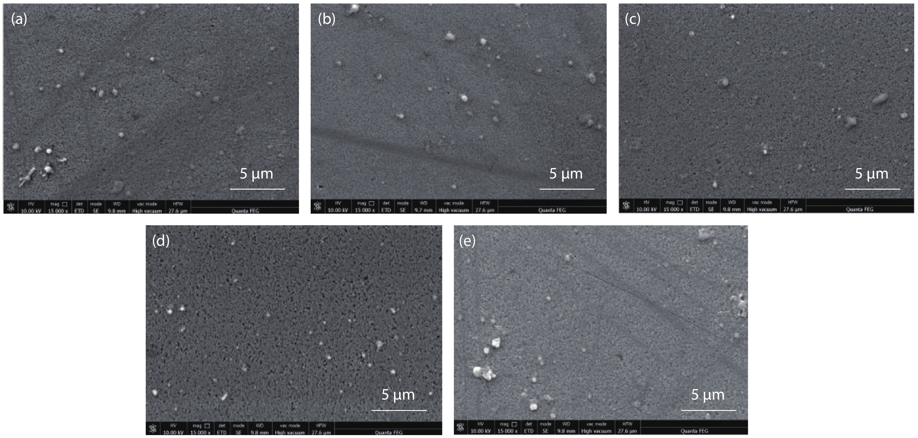
Fig. 1.
SEM images of Cd1–xZnxS thin films prepared with different concentrations of cadmium sulfate.
ARTICLES
Yuming Xue, Shipeng Zhang, Dianyou Song, Liming Zhang, Xinyu Wang, Lang Wang and Hang Sun
Corresponding author: Yuming Xue, orwellx@tjut.edu.cn; Dianyou Song, youdiansong@163.com
Abstract: Cd1–xZnxS thin films were deposited by chemical bath deposition (CBD) on the glass substrate to study the influence of cadmium sulfate concentration on the structural characteristics of the thin film. The SEM results show that the thin film surfaces under the cadmium sulfate concentration of 0.005 M exhibit better compactness and uniformity. The distribution diagrams of thin film elements illustrate the film growth rate changes on the trend of the increase, decrease, and increase with the increase of cadmium sulfate concentration. XRD studies exhibit the crystal structure of the film is the hexagonal phase, and there are obvious diffraction peaks and better crystallinity when the concentration is 0.005 M. Spectrophotometer test results demonstrate that the relationship between zinc content x and optical band gap value Eg can be expressed by the equation Eg(x) = 0.59x2 + 0.69x + 2.43. Increasing the zinc content can increase the optical band gap, and the absorbance of the thin film can be improved by decreasing the cadmium sulfate concentration, however, all of them have good transmittance. At a concentration of 0.005 M, the thin film has good absorbance in the 300–800 nm range, 80% transmittance, and band gap value of 3.24 eV, which is suitable for use as a buffer layer for solar cells.
Keywords: CIGS thin film solar cell, CBD (chemical bath deposition), buffer layer, Cd1–xZnxS thin films, cadmium sulfate
| [1] |
Abza T, Ampong F K, Hone F G, et al. Preparation of cadmium zinc sulfide (Cd1−xZnxS) thin films from acidic chemical baths. Thin Solid Films, 2018, 666, 28 doi: 10.1016/j.tsf.2018.09.011
|
| [2] |
Zellagui R, Dehdouh H, Adnane M, et al. Cd1–xZnxS thin films deposited by chemical bath deposition (CBD) method. Optik, 2020, 207, 164377 doi: 10.1016/j.ijleo.2020.164377
|
| [3] |
Ma L, Ai X, Wu X. Effect of substrate and Zn doping on the structural, optical and electrical properties of CdS thin films prepared by CBD method. J Alloys Compd, 2017, 691, 399 doi: 10.1016/j.jallcom.2016.08.298
|
| [4] |
Bae D, Gho J, Shin M, et al. Effect of zinc addition on properties of cadmium sulfide layer and performance of Cu(In, Ga)Se2 solar cell. Thin Solid Films, 2013, 535, 162 doi: 10.1016/j.tsf.2012.11.077
|
| [5] |
Zhou L M, Li Y L, Dong Y J. Preparation and characterisation of Cd1–xZnxS thin films grown in chemical bath deposition. Mater Res Innov, 2015, 1088, 86 doi: 10.4028/www.scientific.net/AMR.1088.86
|
| [6] |
Guo W, Xue Y M, Gu Y, et al. Influence of solution pH value on structural properties of CdS thin films. J Optoelectron Laser, 2013, 24(11), 2169 doi: 10.16136/j.joel.2013.11.012
|
| [7] |
Oliva A I, Corona J E, PatiñO R, et al. Chemical bath deposition of CdS thin films doped with Zn and Cu. Bull Materials Sci, 2014, 37(2), 247 doi: 10.1007/s12034-014-0642-9
|
| [8] |
Offiah S U, Agbogu A N C, Nwanya A C, et al. Influence of cadmium precursor concentrations on the structural, optical and electrochemical impedance properties of Cd1–xZnxS thin films. Vacuum, 2019, 160, 246 doi: 10.1016/j.vacuum.2018.11.041
|
| [9] |
Yao H, Shen H, Zhu X, et al. Influence of Cd source concentration on photo-current response property of Cd1–xZnxS film prepared by chemical bath deposition. Ceram Int, 2016, 42(2), 2466 doi: 10.1016/j.ceramint.2015.10.047
|
| [10] |
Munna F T, Chelvanathan P, Sobayel K, et al. Effect of zinc doping on the optoelectronic properties of cadmium sulphide (CdS) thin films deposited by chemical bath deposition by utilising an alternative sulphur precursor. Optik, 2020, 218, 165197 doi: 10.1016/j.ijleo.2020.165197
|
| [11] |
Carreón-Moncada I, González L A, Pech-Canul M I, et al. Cd1–xZnxS thin films with low Zn content obtained by an ammonia-free chemical bath deposition process. Thin Solid Films, 2013, 548, 270 doi: 10.1016/j.tsf.2013.10.024
|
| [12] |
Liu J, Wei A, Zhao Y. Effect of different complexing agents on the properties of chemical-bath-deposited ZnS thin films. J Alloys Compd, 2014, 588, 228 doi: 10.1016/j.jallcom.2013.11.042
|
| [13] |
Kaleli M. Effect of sulphurization and Al doping on Cd0.25Zn0.75S thin films deposited by ultrasonic spray pyrolysis technique. Optik, 2019, 207, 163781 doi: 10.1016/j.ijleo.2019.163781
|
| [14] |
Zhou Z, Guo L. Cd1–xZnxS energy band calculated by the first-principle method. Journal of Xi'an Jiaotong University, 2008, 42(2), 248
|
| [15] |
Salem A M. Structure, refractive-index dispersion and the optical absorption edge of chemically deposited ZnxCd1–xS thin films. Appl Phys A, 2002, 74(2), 205 doi: 10.1007/s003390100877
|
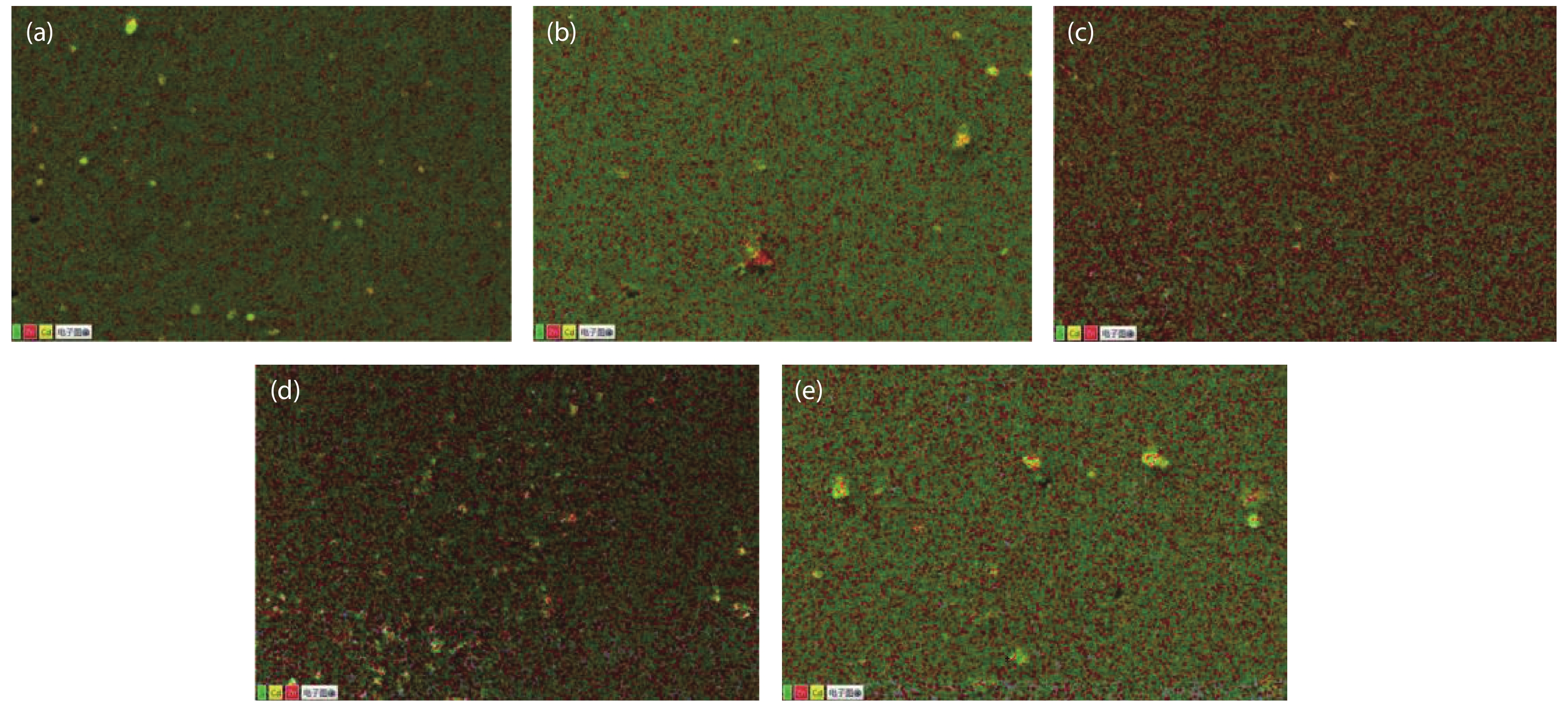
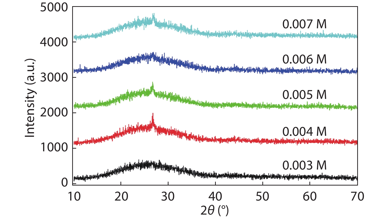
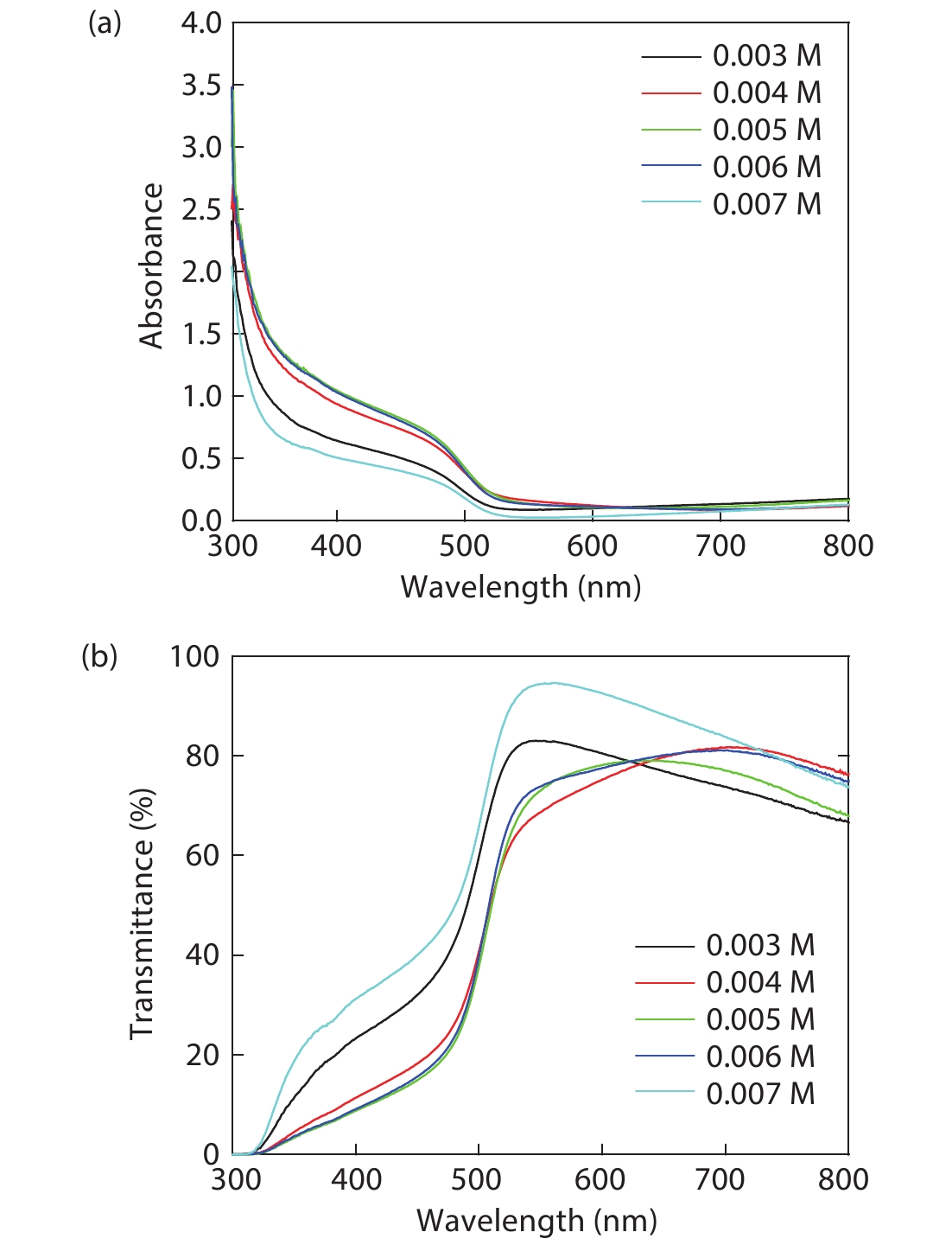
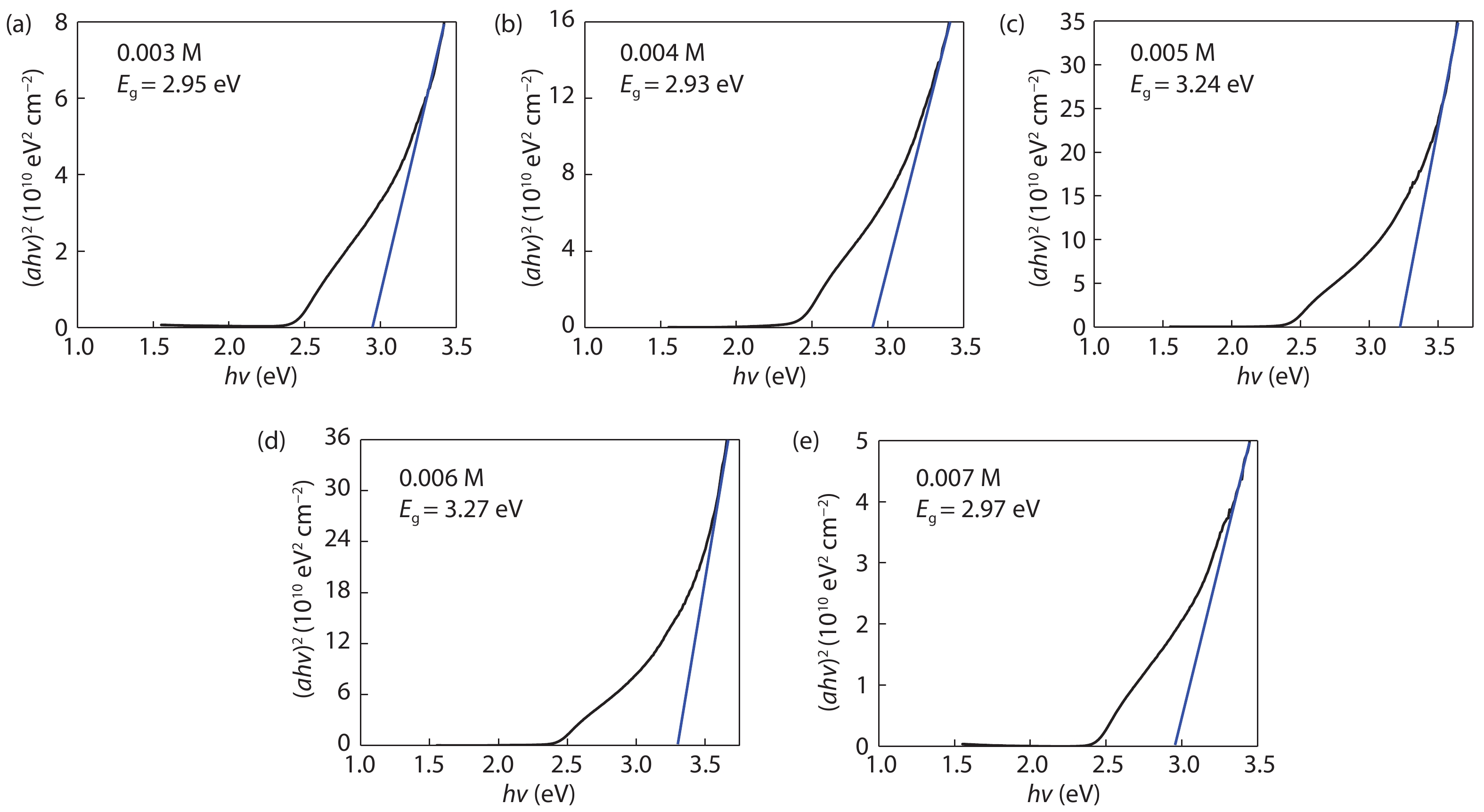
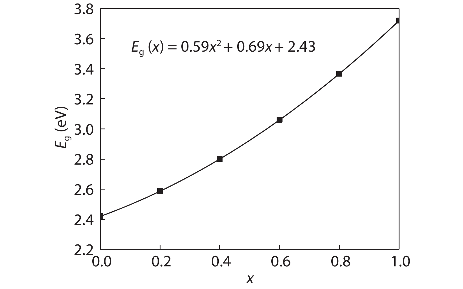
Table 1. Deposition conditions of CBD-Cd1–xZnxS.
| Reagent | Concentration (M) |
| ZnSO4 | 0.020 |
| (NH4)2SO4 | 0.025 |
| SC(NH2)2 | 0.015 |
| NH3·H2O | 25% |
| CdSO4 | 0.003, 0.004, 0.005, 0.006, 0.007 |
 DownLoad: CSV
Table 2. Thickness of Cd1–xZnxS thin films with different cadmium sulfate concentration.
| Concentration of cadmium sulfate (M) | Thickness (nm) |
| 0.003 | 71.13 |
| 0.004 | 73.28 |
| 0.005 | 64.73 |
| 0.006 | 62.46 |
| 0.007 | 66.51 |
DownLoad: CSV
Table 3. The atom ratios of S, Zn and Cd in Cd1–xZnxS thin films prepared with different concentrations of cadmium sulfate.
| Concentration of cadmium sulfate (M) | Atom ratio of S, Zn and Cd | Zn/(Zn+Cd) |
| 0.003 | 30.40 : 36.81 : 32.79 | 0.529 |
| 0.004 | 31.87 : 34.34 : 33.79 | 0.504 |
| 0.005 | 22.17 : 55.83 : 22.00 | 0.717 |
| 0.006 | 22.61 : 57.24 : 20.15 | 0.739 |
| 0.007 | 28.82 : 37.92 : 33.26 | 0.533 |
DownLoad: CSV
Table 4. Film element content, zinc-cadmium content ratio and band gap.
| Cd (at.%) | Zn (at.%) | S (at.%) | Zn/Cd | Cd1–xZnxS | Eg (eV) |
| 32.79 | 36.81 | 30.40 | 1.12 | Cd0.48Zn0.52S | 2.95 |
| 33.79 | 34.34 | 31.87 | 1.02 | Cd0.50Zn0.50S | 2.93 |
| 22.00 | 55.83 | 22.17 | 2.54 | Cd0.28Zn0.72S | 3.24 |
| 20.15 | 57.24 | 22.61 | 2.84 | Cd0.26Zn0.74S | 3.27 |
| 33.26 | 37.92 | 28.82 | 1.14 | Cd0.47Zn0.53S | 2.97 |
DownLoad: CSV
| [1] |
Abza T, Ampong F K, Hone F G, et al. Preparation of cadmium zinc sulfide (Cd1−xZnxS) thin films from acidic chemical baths. Thin Solid Films, 2018, 666, 28 doi: 10.1016/j.tsf.2018.09.011
|
| [2] |
Zellagui R, Dehdouh H, Adnane M, et al. Cd1–xZnxS thin films deposited by chemical bath deposition (CBD) method. Optik, 2020, 207, 164377 doi: 10.1016/j.ijleo.2020.164377
|
| [3] |
Ma L, Ai X, Wu X. Effect of substrate and Zn doping on the structural, optical and electrical properties of CdS thin films prepared by CBD method. J Alloys Compd, 2017, 691, 399 doi: 10.1016/j.jallcom.2016.08.298
|
| [4] |
Bae D, Gho J, Shin M, et al. Effect of zinc addition on properties of cadmium sulfide layer and performance of Cu(In, Ga)Se2 solar cell. Thin Solid Films, 2013, 535, 162 doi: 10.1016/j.tsf.2012.11.077
|
| [5] |
Zhou L M, Li Y L, Dong Y J. Preparation and characterisation of Cd1–xZnxS thin films grown in chemical bath deposition. Mater Res Innov, 2015, 1088, 86 doi: 10.4028/www.scientific.net/AMR.1088.86
|
| [6] |
Guo W, Xue Y M, Gu Y, et al. Influence of solution pH value on structural properties of CdS thin films. J Optoelectron Laser, 2013, 24(11), 2169 doi: 10.16136/j.joel.2013.11.012
|
| [7] |
Oliva A I, Corona J E, PatiñO R, et al. Chemical bath deposition of CdS thin films doped with Zn and Cu. Bull Materials Sci, 2014, 37(2), 247 doi: 10.1007/s12034-014-0642-9
|
| [8] |
Offiah S U, Agbogu A N C, Nwanya A C, et al. Influence of cadmium precursor concentrations on the structural, optical and electrochemical impedance properties of Cd1–xZnxS thin films. Vacuum, 2019, 160, 246 doi: 10.1016/j.vacuum.2018.11.041
|
| [9] |
Yao H, Shen H, Zhu X, et al. Influence of Cd source concentration on photo-current response property of Cd1–xZnxS film prepared by chemical bath deposition. Ceram Int, 2016, 42(2), 2466 doi: 10.1016/j.ceramint.2015.10.047
|
| [10] |
Munna F T, Chelvanathan P, Sobayel K, et al. Effect of zinc doping on the optoelectronic properties of cadmium sulphide (CdS) thin films deposited by chemical bath deposition by utilising an alternative sulphur precursor. Optik, 2020, 218, 165197 doi: 10.1016/j.ijleo.2020.165197
|
| [11] |
Carreón-Moncada I, González L A, Pech-Canul M I, et al. Cd1–xZnxS thin films with low Zn content obtained by an ammonia-free chemical bath deposition process. Thin Solid Films, 2013, 548, 270 doi: 10.1016/j.tsf.2013.10.024
|
| [12] |
Liu J, Wei A, Zhao Y. Effect of different complexing agents on the properties of chemical-bath-deposited ZnS thin films. J Alloys Compd, 2014, 588, 228 doi: 10.1016/j.jallcom.2013.11.042
|
| [13] |
Kaleli M. Effect of sulphurization and Al doping on Cd0.25Zn0.75S thin films deposited by ultrasonic spray pyrolysis technique. Optik, 2019, 207, 163781 doi: 10.1016/j.ijleo.2019.163781
|
| [14] |
Zhou Z, Guo L. Cd1–xZnxS energy band calculated by the first-principle method. Journal of Xi'an Jiaotong University, 2008, 42(2), 248
|
| [15] |
Salem A M. Structure, refractive-index dispersion and the optical absorption edge of chemically deposited ZnxCd1–xS thin films. Appl Phys A, 2002, 74(2), 205 doi: 10.1007/s003390100877
|


Article views: 3765 Times PDF downloads: 79 Times Cited by: 0 Times
Received: 12 April 2021 Revised: 20 April 2021 Online: Accepted Manuscript: 10 June 2021Uncorrected proof: 11 June 2021Published: 01 November 2021
| Citation: |
Yuming Xue, Shipeng Zhang, Dianyou Song, Liming Zhang, Xinyu Wang, Lang Wang, Hang Sun. Effect of concentration of cadmium sulfate solution on structural, optical and electric properties of Cd1–xZnxS thin films[J]. Journal of Semiconductors, 2021, 42(11): 112101. doi: 10.1088/1674-4926/42/11/112101
****
Y M Xue, S P Zhang, D Y Song, L M Zhang, X Y Wang, L Wang, H Sun, Effect of concentration of cadmium sulfate solution on structural, optical and electric properties of Cd1–xZnxS thin films[J]. J. Semicond., 2021, 42(11): 112101. doi: 10.1088/1674-4926/42/11/112101.

|
| [1] |
Abza T, Ampong F K, Hone F G, et al. Preparation of cadmium zinc sulfide (Cd1−xZnxS) thin films from acidic chemical baths. Thin Solid Films, 2018, 666, 28 doi: 10.1016/j.tsf.2018.09.011
|
| [2] |
Zellagui R, Dehdouh H, Adnane M, et al. Cd1–xZnxS thin films deposited by chemical bath deposition (CBD) method. Optik, 2020, 207, 164377 doi: 10.1016/j.ijleo.2020.164377
|
| [3] |
Ma L, Ai X, Wu X. Effect of substrate and Zn doping on the structural, optical and electrical properties of CdS thin films prepared by CBD method. J Alloys Compd, 2017, 691, 399 doi: 10.1016/j.jallcom.2016.08.298
|
| [4] |
Bae D, Gho J, Shin M, et al. Effect of zinc addition on properties of cadmium sulfide layer and performance of Cu(In, Ga)Se2 solar cell. Thin Solid Films, 2013, 535, 162 doi: 10.1016/j.tsf.2012.11.077
|
| [5] |
Zhou L M, Li Y L, Dong Y J. Preparation and characterisation of Cd1–xZnxS thin films grown in chemical bath deposition. Mater Res Innov, 2015, 1088, 86 doi: 10.4028/www.scientific.net/AMR.1088.86
|
| [6] |
Guo W, Xue Y M, Gu Y, et al. Influence of solution pH value on structural properties of CdS thin films. J Optoelectron Laser, 2013, 24(11), 2169 doi: 10.16136/j.joel.2013.11.012
|
| [7] |
Oliva A I, Corona J E, PatiñO R, et al. Chemical bath deposition of CdS thin films doped with Zn and Cu. Bull Materials Sci, 2014, 37(2), 247 doi: 10.1007/s12034-014-0642-9
|
| [8] |
Offiah S U, Agbogu A N C, Nwanya A C, et al. Influence of cadmium precursor concentrations on the structural, optical and electrochemical impedance properties of Cd1–xZnxS thin films. Vacuum, 2019, 160, 246 doi: 10.1016/j.vacuum.2018.11.041
|
| [9] |
Yao H, Shen H, Zhu X, et al. Influence of Cd source concentration on photo-current response property of Cd1–xZnxS film prepared by chemical bath deposition. Ceram Int, 2016, 42(2), 2466 doi: 10.1016/j.ceramint.2015.10.047
|
| [10] |
Munna F T, Chelvanathan P, Sobayel K, et al. Effect of zinc doping on the optoelectronic properties of cadmium sulphide (CdS) thin films deposited by chemical bath deposition by utilising an alternative sulphur precursor. Optik, 2020, 218, 165197 doi: 10.1016/j.ijleo.2020.165197
|
| [11] |
Carreón-Moncada I, González L A, Pech-Canul M I, et al. Cd1–xZnxS thin films with low Zn content obtained by an ammonia-free chemical bath deposition process. Thin Solid Films, 2013, 548, 270 doi: 10.1016/j.tsf.2013.10.024
|
| [12] |
Liu J, Wei A, Zhao Y. Effect of different complexing agents on the properties of chemical-bath-deposited ZnS thin films. J Alloys Compd, 2014, 588, 228 doi: 10.1016/j.jallcom.2013.11.042
|
| [13] |
Kaleli M. Effect of sulphurization and Al doping on Cd0.25Zn0.75S thin films deposited by ultrasonic spray pyrolysis technique. Optik, 2019, 207, 163781 doi: 10.1016/j.ijleo.2019.163781
|
| [14] |
Zhou Z, Guo L. Cd1–xZnxS energy band calculated by the first-principle method. Journal of Xi'an Jiaotong University, 2008, 42(2), 248
|
| [15] |
Salem A M. Structure, refractive-index dispersion and the optical absorption edge of chemically deposited ZnxCd1–xS thin films. Appl Phys A, 2002, 74(2), 205 doi: 10.1007/s003390100877
|

 WeChat ID
Journal of Semiconductors © 2017 All Rights Reserved 京ICP备05085259号-2


