ARTICLES

Enhancement of refresh time in quasi-nonvolatile memory by the density of states engineering

Zhaowu Tang1, Chunsen Liu1, 2, , Senfeng Zeng1, Xiaohe Huang1, Liwei Liu1, Jiayi Li1, Yugang Jiang2, David Wei Zhang1 and Peng Zhou1,

+ Author Affiliations

 Corresponding author: Chunsen Liu, chunsen_liu@fudan.edu.cn; Peng Zhou, pengzhou@fudan.edu.cn

PDF

Turn off MathJax

Abstract: The recently reported quasi-nonvolatile memory based on semi-floating gate architecture has attracted extensive attention thanks to its potential to bridge the large gap between volatile and nonvolatile memory. However, the further extension of the refresh time in quasi-nonvolatile memory is limited by the charge leakage through the p–n junction. Here, based on the density of states engineered van der Waals heterostructures, the leakage of electrons from the floating gate to the channel is greatly suppressed. As a result, the refresh time is effectively extended to more than 100 s, which is the longest among all previously reported quasi-nonvolatile memories. This work provides a new idea to enhance the refresh time of quasi-nonvolatile memory by the density of states engineering and demonstrates great application potential for high-speed and low-power memory technology.

Key words: quasi-nonvolatile memoryrefresh timedensity of states engineering


[1]
Liu C, Yan X, Song X, et al. A semi-floating gate memory based on van der Waals heterostructures for quasi-non-volatile applications. Nat Nanotechnol, 2018, 13(5), 404 doi: 10.1038/s41565-018-0102-6
[2]
Novoselov K S, Geim A K, Morozov S V, et al. Electric field effect in atomically thin carbon films. Science, 2004, 306(5696), 666 doi: 10.1126/science.1102896
[3]
Qiu C, Liu F, Xu L, et al. Dirac-source field-effect transistors as energy-efficient, high-performance electronic switches. Science, 2018, 361(6400), 387 doi: 10.1126/science.aap9195
[4]
Liu F, Qiu C, Zhang Z, et al. Dirac electrons at the source: breaking the 60-mV/decade switching limit. IEEE Trans Electron Devices, 2018, 65(7), 2736 doi: 10.1109/TED.2018.2836387
[5]
Liu F, Qiu C, Zhang Z, et al. First principles simulation of energy efficient switching by source density of states engineering. IEEE International Electron Devices Meeting (IEDM), 2018, 33
[6]
Lyu J, Pei J, Guo Y, et al. A new opportunity for 2D van der Waals heterostructures: making steep-slope transistors. Adv Mater, 2020, 32(2), 1906000 doi: 10.1002/adma.201906000
[7]
Yu W J, Chae S H, Lee S Y, et al. Ultra-transparent, flexible single-walled carbon nanotube non-volatile memory device with an oxygen-decorated graphene electrode. Adv Mater, 2011, 23(16), 1889 doi: 10.1002/adma.201004444
[8]
Lee S, Song E B, Kim S, et al. Impact of gate work-function on memory characteristics in Al2O3/HfOx/Al2O3/graphene charge-trap memory devices. Appl Phys Lett, 2012, 100(2), 023109 doi: 10.1063/1.3675633
[9]
Kim S M, Song E B, Lee S, et al. Transparent and flexible graphene charge-trap memory. ACS Nano, 2012, 6(9), 7879 doi: 10.1021/nn302193q
[10]
Bertolazzi S, Krasnozhon D, Kis A. Nonvolatile memory cells based on MoS2/graphene heterostructures. ACS Nano, 2013, 7(4), 3246 doi: 10.1021/nn3059136
[11]
Choi M S, Lee G H, Yu Y J, et al. Controlled charge trapping by molybdenum disulphide and graphene in ultrathin heterostructured memory devices. Nat Commun, 2013, 4(1), 1624 doi: 10.1038/ncomms2652
[12]
Zhang E, Wang W, Zhang C, et al. Tunable charge-trap memory based on few-layer MoS2. ACS Nano, 2015, 9(1), 612 doi: 10.1021/nn5059419
[13]
Vu Q A, Shin Y S, Kim Y R, et al. Two-terminal floating-gate memory with van der Waals heterostructures for ultrahigh on/off ratio. Nat Commun, 2016, 7(1), 12725 doi: 10.1038/ncomms12725
[14]
He G, Ramamoorthy H, Kwan C P, et al. Thermally assisted nonvolatile memory in monolayer MoS2 transistors. Nano Lett, 2016, 16(10), 6445 doi: 10.1021/acs.nanolett.6b02905
[15]
Lee Y T, Kwon H, Kim J S, et al. Nonvolatile ferroelectric memory circuit using black phosphorus nanosheet-based field-effect transistors with P(VDF-TrFE) polymer. ACS Nano, 2015, 9(10), 10394 doi: 10.1021/acsnano.5b04592
[16]
Hou X, Zhang H, Liu C, et al. Charge-trap memory based on hybrid 0D quantum dot-2D WSe2 structure. Small, 2018, 14(20), 1800319 doi: 10.1002/smll.201800319
[17]
Mishra A, Janardanan A, Khare M, et al. Reduced multilayer graphene oxide floating gate flash memory with large memory window and robust retention characteristics. IEEE Electron Device Lett, 2013, 34(9), 1136 doi: 10.1109/LED.2013.2272643
[18]
Ding Y, Liu L, Li J, et al. A semi-floating memory with 535% enhancement of refresh time by local field modulation. Adv Funct Mater, 2020, 30(15), 1908089 doi: 10.1002/adfm.201908089
[19]
Li J, Liu L, Chen X, et al. Symmetric ultrafast writing and erasing speeds in quasi-nonvolatile memory via van der Waals heterostructures. Adv Mater, 2019, 31(11), 1808035 doi: 10.1002/adma.201808035
[20]
Wu G, Tian B, Liu L, et al. Programmable transition metal dichalcogenide homojunctions controlled by nonvolatile ferroelectric domains. Nat Electron, 2020, 3(1), 43 doi: 10.1038/s41928-019-0350-y
[21]
Liu C, Zhou P. Memory Devices Based on Van der Waals Heterostructures. ACS Mater Lett, 2020, 2(9), 1101 doi: 10.1021/acsmaterialslett.0c00227
[22]
Liu J, Huang Z, Lai F, et al. Controllable growth of the graphene from millimeter-sized monolayer to multilayer on Cu by chemical vapor deposition. Nanoscale Res Lett, 2015, 10(1), 455 doi: 10.1186/s11671-015-1164-0
[23]
Dai G P, Wu M H, Taylor D K, et al. Hybrid 3D graphene and aligned carbon nanofiber array architectures. RSC Adv, 2012, 2(24), 8965 doi: 10.1039/c2ra21084c
[24]
Cao Y, Wang Z, Bian Q, et al. Phonon modes and photonic excitation transitions of MoS2 induced by top-deposited graphene revealed by Raman spectroscopy and photoluminescence. Appl Phys Lett, 2019, 114(13), 133103 doi: 10.1063/1.5083104
[25]
Mouri S, Miyauchi Y, Matsuda K. Tunable photoluminescence of monolayer MoS2 via chemical doping. Nano Lett, 2013, 13(12), 5944 doi: 10.1021/nl403036h
[26]
Ahn G H, Amani M, Rasool H, et al. Strain-engineered growth of two-dimensional materials. Nat Commun, 2017, 8(1), 608 doi: 10.1038/s41467-017-00516-5
Fig. 1.  (Color online) The schematic and characterization of the QNV memory. (a) The linearly varied density of states DOS(E), super-exponentially decreased electron density n(E) with the energy of Gr Dirac material, and the cut-off of electron injection from Gr Dirac material to channel over the bulk barrier $\phi $B. The orange dashed line in n(E) represents the Boltzmann distribution. (b) The schematic structure of the QNV memory in which MoS2 serves as the channel, Gr-hBN servers as the semi-blocking layer, and WSe2 serves as the floating gate. (c) The false-colored optical microscope image of the device. The scale bar is 5 μm. (d) The Raman spectra of monolayer Gr and multilayer MoS2 and WSe2 were measured by using a 532 nm solid-state laser. (e) The double sweep transfer characteristic of the QNV memory under VDS = 0.5 V. A large Ion/Ioff exceeding 104 is achieved when reading at VG = 0 V. The inset is the full measurement range (VG varying from –2 to 2 V) of transfer characteristics on a logarithmic scale.

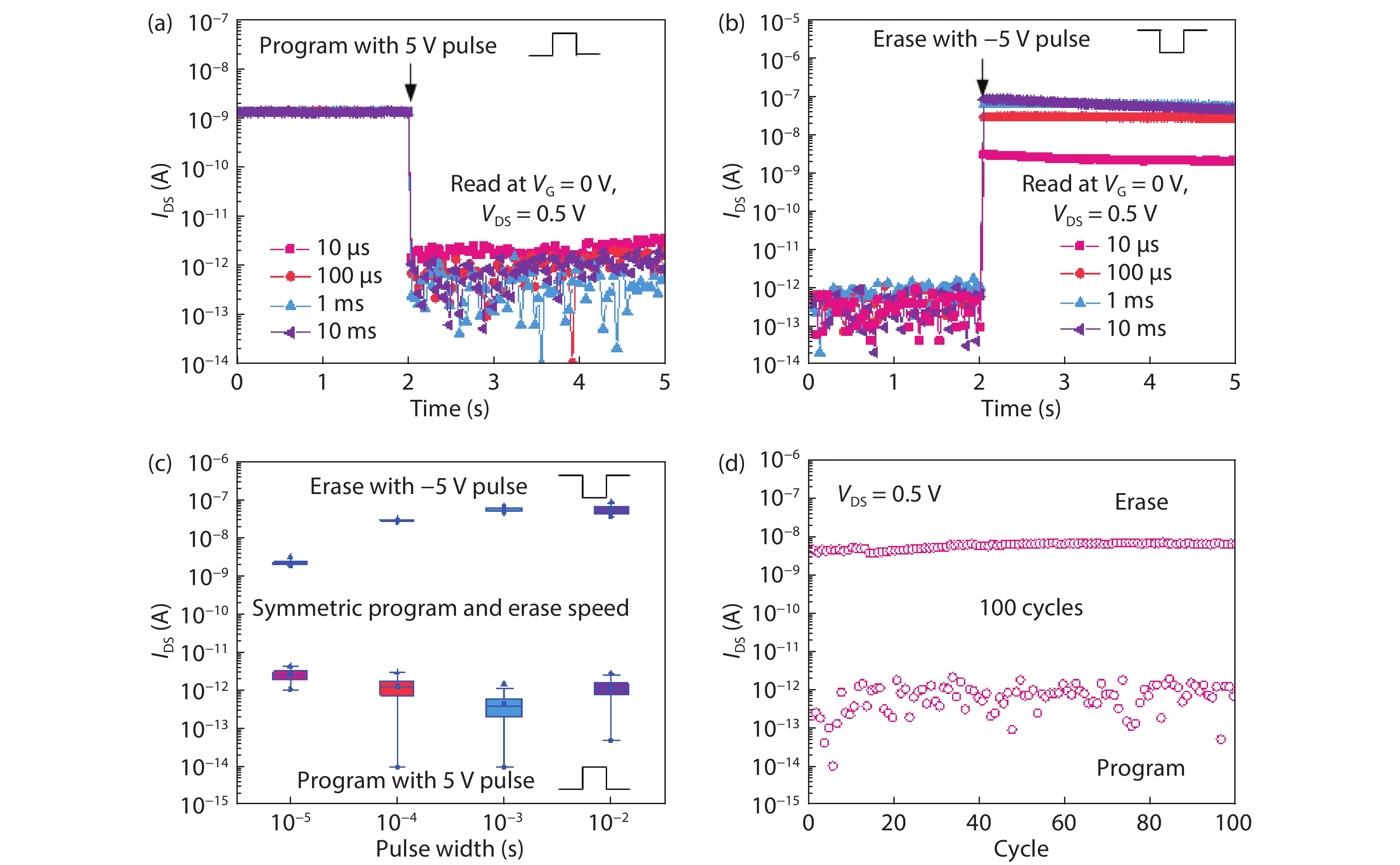
Fig. 2.  (Color online) The symmetric ultrafast programming and erasing operation of the QNV memory. (a) The initial state is state-1 and the 5 V gate voltage pulse with different pulse widths is applied for the programming operation. After that, the reading operation is carried out at VG = 0 V and VDS = 0.5 V. (b) The initial state is state-0 after applying a positive gate voltage pulse for programming and the –5 V gate voltage pulse with different pulse width is applied for the erasing operation. After that the reading operation is carried out at VG = 0 V and VDS = 0.5 V. (c) The current state after the programming and erasing operations with different pulse width gate voltage pulse (the pulse amplitude is fixed 5 V). The data points of the current state are the mean value of the sampling points produced while monitoring the channel current 5 s after the programming/erasing operation. (d) The endurance of the device for 100 cycles of the programming/erasing pulse, demonstrating that no performance degradation was observed.

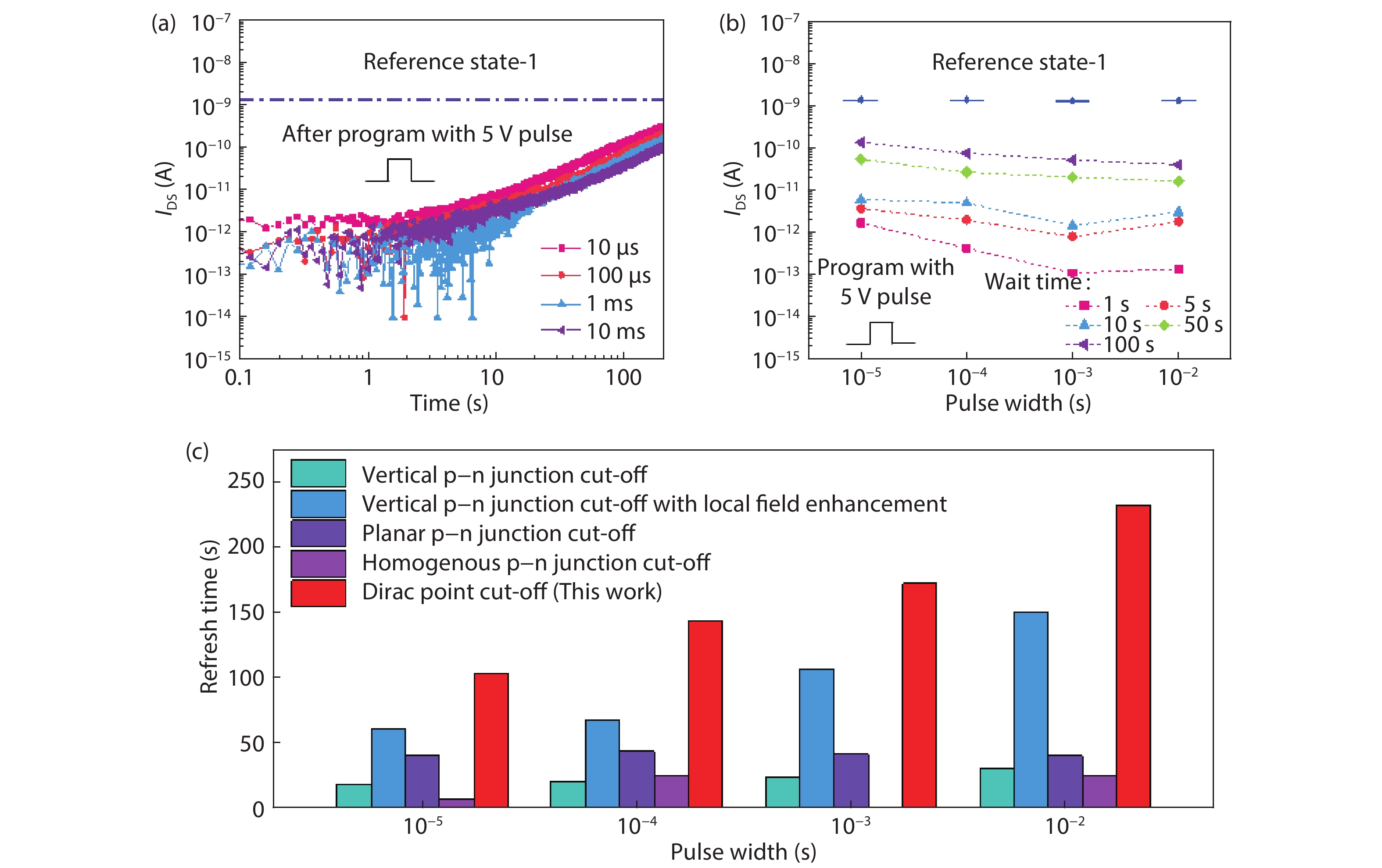
Fig. 3.  (Color online) The data retention ability of the QNV memory. (a) The retention characteristic of the memory after the programming operation with different gate pulse widths (the pulse amplitude is fixed 5 V). (b) The relationship between the state-0 output current and program pulse width for different wait times. (c) The comparison of the refresh time of our device with the other QNV memory devices[1, 1820] under different pulse widths.

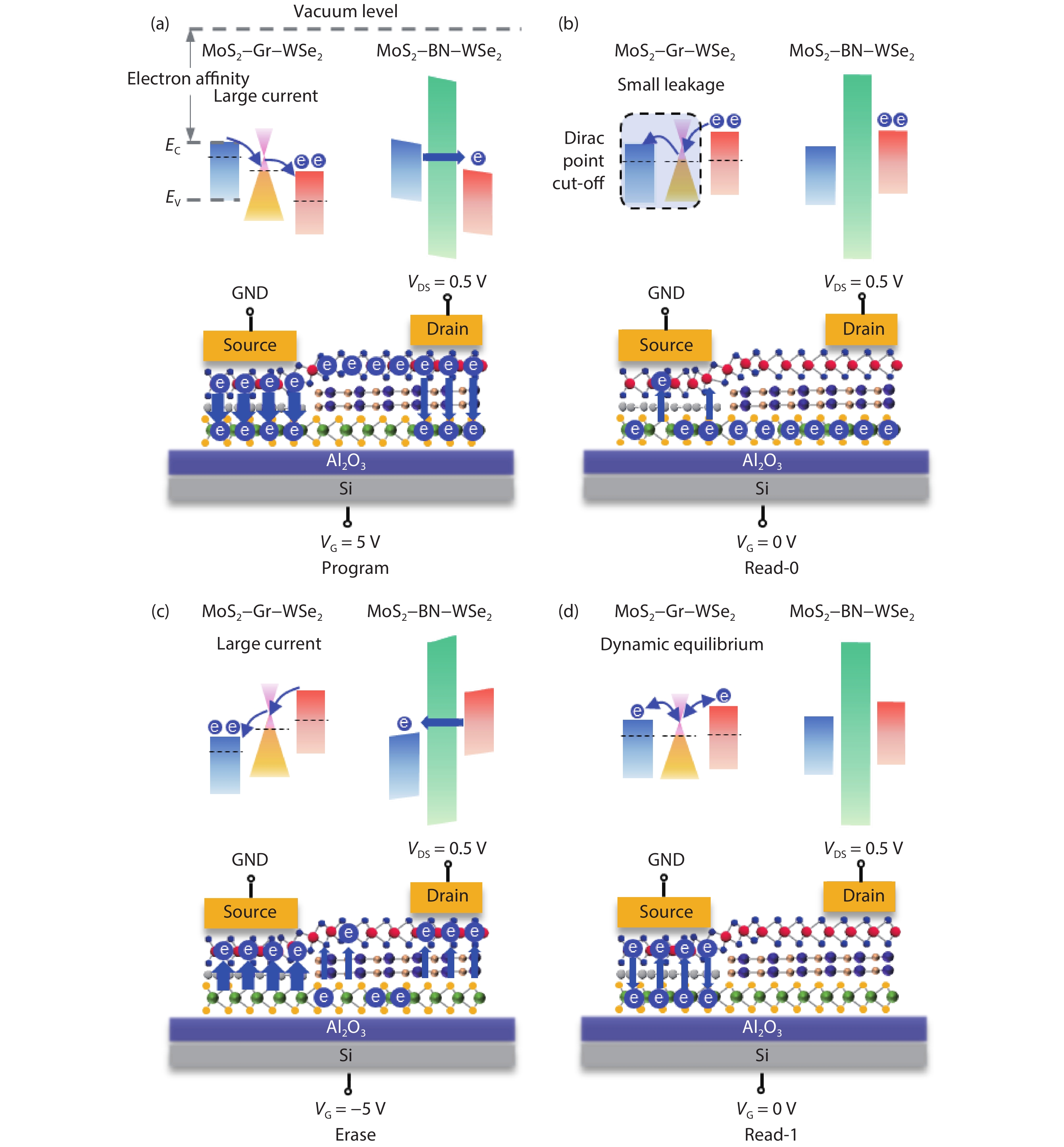
Fig. 4.  (Color online) The schematic illustrations of the band diagrams and charges transport in the QNV memory at different operation modes: (a) program, (b) read-0, (c) erase, and (d) read-1. The blue balls and arrows represent the electrons and electron flow direction, respectively. The approximate electron affinities of MoS2 and WSe2 are 4.0–4.2, 3.5–4.0 eV respectively, and the work function of monolayer Gr is ~4.3 eV.

[1]
Liu C, Yan X, Song X, et al. A semi-floating gate memory based on van der Waals heterostructures for quasi-non-volatile applications. Nat Nanotechnol, 2018, 13(5), 404 doi: 10.1038/s41565-018-0102-6
[2]
Novoselov K S, Geim A K, Morozov S V, et al. Electric field effect in atomically thin carbon films. Science, 2004, 306(5696), 666 doi: 10.1126/science.1102896
[3]
Qiu C, Liu F, Xu L, et al. Dirac-source field-effect transistors as energy-efficient, high-performance electronic switches. Science, 2018, 361(6400), 387 doi: 10.1126/science.aap9195
[4]
Liu F, Qiu C, Zhang Z, et al. Dirac electrons at the source: breaking the 60-mV/decade switching limit. IEEE Trans Electron Devices, 2018, 65(7), 2736 doi: 10.1109/TED.2018.2836387
[5]
Liu F, Qiu C, Zhang Z, et al. First principles simulation of energy efficient switching by source density of states engineering. IEEE International Electron Devices Meeting (IEDM), 2018, 33
[6]
Lyu J, Pei J, Guo Y, et al. A new opportunity for 2D van der Waals heterostructures: making steep-slope transistors. Adv Mater, 2020, 32(2), 1906000 doi: 10.1002/adma.201906000
[7]
Yu W J, Chae S H, Lee S Y, et al. Ultra-transparent, flexible single-walled carbon nanotube non-volatile memory device with an oxygen-decorated graphene electrode. Adv Mater, 2011, 23(16), 1889 doi: 10.1002/adma.201004444
[8]
Lee S, Song E B, Kim S, et al. Impact of gate work-function on memory characteristics in Al2O3/HfOx/Al2O3/graphene charge-trap memory devices. Appl Phys Lett, 2012, 100(2), 023109 doi: 10.1063/1.3675633
[9]
Kim S M, Song E B, Lee S, et al. Transparent and flexible graphene charge-trap memory. ACS Nano, 2012, 6(9), 7879 doi: 10.1021/nn302193q
[10]
Bertolazzi S, Krasnozhon D, Kis A. Nonvolatile memory cells based on MoS2/graphene heterostructures. ACS Nano, 2013, 7(4), 3246 doi: 10.1021/nn3059136
[11]
Choi M S, Lee G H, Yu Y J, et al. Controlled charge trapping by molybdenum disulphide and graphene in ultrathin heterostructured memory devices. Nat Commun, 2013, 4(1), 1624 doi: 10.1038/ncomms2652
[12]
Zhang E, Wang W, Zhang C, et al. Tunable charge-trap memory based on few-layer MoS2. ACS Nano, 2015, 9(1), 612 doi: 10.1021/nn5059419
[13]
Vu Q A, Shin Y S, Kim Y R, et al. Two-terminal floating-gate memory with van der Waals heterostructures for ultrahigh on/off ratio. Nat Commun, 2016, 7(1), 12725 doi: 10.1038/ncomms12725
[14]
He G, Ramamoorthy H, Kwan C P, et al. Thermally assisted nonvolatile memory in monolayer MoS2 transistors. Nano Lett, 2016, 16(10), 6445 doi: 10.1021/acs.nanolett.6b02905
[15]
Lee Y T, Kwon H, Kim J S, et al. Nonvolatile ferroelectric memory circuit using black phosphorus nanosheet-based field-effect transistors with P(VDF-TrFE) polymer. ACS Nano, 2015, 9(10), 10394 doi: 10.1021/acsnano.5b04592
[16]
Hou X, Zhang H, Liu C, et al. Charge-trap memory based on hybrid 0D quantum dot-2D WSe2 structure. Small, 2018, 14(20), 1800319 doi: 10.1002/smll.201800319
[17]
Mishra A, Janardanan A, Khare M, et al. Reduced multilayer graphene oxide floating gate flash memory with large memory window and robust retention characteristics. IEEE Electron Device Lett, 2013, 34(9), 1136 doi: 10.1109/LED.2013.2272643
[18]
Ding Y, Liu L, Li J, et al. A semi-floating memory with 535% enhancement of refresh time by local field modulation. Adv Funct Mater, 2020, 30(15), 1908089 doi: 10.1002/adfm.201908089
[19]
Li J, Liu L, Chen X, et al. Symmetric ultrafast writing and erasing speeds in quasi-nonvolatile memory via van der Waals heterostructures. Adv Mater, 2019, 31(11), 1808035 doi: 10.1002/adma.201808035
[20]
Wu G, Tian B, Liu L, et al. Programmable transition metal dichalcogenide homojunctions controlled by nonvolatile ferroelectric domains. Nat Electron, 2020, 3(1), 43 doi: 10.1038/s41928-019-0350-y
[21]
Liu C, Zhou P. Memory Devices Based on Van der Waals Heterostructures. ACS Mater Lett, 2020, 2(9), 1101 doi: 10.1021/acsmaterialslett.0c00227
[22]
Liu J, Huang Z, Lai F, et al. Controllable growth of the graphene from millimeter-sized monolayer to multilayer on Cu by chemical vapor deposition. Nanoscale Res Lett, 2015, 10(1), 455 doi: 10.1186/s11671-015-1164-0
[23]
Dai G P, Wu M H, Taylor D K, et al. Hybrid 3D graphene and aligned carbon nanofiber array architectures. RSC Adv, 2012, 2(24), 8965 doi: 10.1039/c2ra21084c
[24]
Cao Y, Wang Z, Bian Q, et al. Phonon modes and photonic excitation transitions of MoS2 induced by top-deposited graphene revealed by Raman spectroscopy and photoluminescence. Appl Phys Lett, 2019, 114(13), 133103 doi: 10.1063/1.5083104
[25]
Mouri S, Miyauchi Y, Matsuda K. Tunable photoluminescence of monolayer MoS2 via chemical doping. Nano Lett, 2013, 13(12), 5944 doi: 10.1021/nl403036h
[26]
Ahn G H, Amani M, Rasool H, et al. Strain-engineered growth of two-dimensional materials. Nat Commun, 2017, 8(1), 608 doi: 10.1038/s41467-017-00516-5

21010012suppl.pdf

  • Search

    Advanced Search >>

    GET CITATION

    shu

    Export: BibTex EndNote

    Article Metrics

    Article views: 3280 Times PDF downloads: 51 Times Cited by: 0 Times

    History

    Received: 08 January 2021 Revised: 13 January 2021 Online: Accepted Manuscript: 20 January 2021Uncorrected proof: 22 January 2021Published: 08 February 2021

    Catalog

      Email This Article

      User name:
      Email:*请输入正确邮箱
      Code:*验证码错误
      Zhaowu Tang, Chunsen Liu, Senfeng Zeng, Xiaohe Huang, Liwei Liu, Jiayi Li, Yugang Jiang, David Wei Zhang, Peng Zhou. Enhancement of refresh time in quasi-nonvolatile memory by the density of states engineering[J]. Journal of Semiconductors, 2021, 42(2): 024101. doi: 10.1088/1674-4926/42/2/024101 ****Zhaowu Tang, Chunsen Liu, Senfeng Zeng, Xiaohe Huang, Liwei Liu, Jiayi Li, Yugang Jiang, David Wei Zhang, Peng Zhou. 2021: Enhancement of refresh time in quasi-nonvolatile memory by the density of states engineering. Journal of Semiconductors, 42(2): 024101. doi: 10.1088/1674-4926/42/2/024101
      Citation:
      Zhaowu Tang, Chunsen Liu, Senfeng Zeng, Xiaohe Huang, Liwei Liu, Jiayi Li, Yugang Jiang, David Wei Zhang, Peng Zhou. Enhancement of refresh time in quasi-nonvolatile memory by the density of states engineering[J]. Journal of Semiconductors, 2021, 42(2): 024101. doi: 10.1088/1674-4926/42/2/024101 ****
      Zhaowu Tang, Chunsen Liu, Senfeng Zeng, Xiaohe Huang, Liwei Liu, Jiayi Li, Yugang Jiang, David Wei Zhang, Peng Zhou. 2021: Enhancement of refresh time in quasi-nonvolatile memory by the density of states engineering. Journal of Semiconductors, 42(2): 024101. doi: 10.1088/1674-4926/42/2/024101

      Enhancement of refresh time in quasi-nonvolatile memory by the density of states engineering

      doi: 10.1088/1674-4926/42/2/024101
      More Information
      • Zhaowu Tang:was born in Hunan Province, China, in 1998. He received a B.E. degree in materials science and engineering from Northwestern Polytechnical University, China, in 2019. He is a currently graduate student of School of Microelectronics in Fudan University, China. His research interests include 2D materials and their application in logic devices and memory devices. Mr. Tang’s awards and honors include Fudan University Outstanding Academic Scholarship and Huawei Scholarship
      • Chunsen Liu:received the B.S. degree in School of Electronic Science and Technology from Jilin University, Jilin, China, in 2015 and the Ph.D. degree in school of microelectronics from Fudan University, Shanghai, China, in 2019. He is currently working in computer science at Fudan University. His research interest includes the innovation of new logic and memory devices, and exploration of new electronic system architecture. He has first-authored several journal papers in Nature Nanotechnology, Small, etc
      • Peng Zhou:received his bachelor and Ph.D. degree in physics from Fudan University, Shanghai, China, in 2000 and 2005, respectively. He is currently a full professor on novel electronic devices and process in School of Microelectronics, Fudan University. He has authored or co-authored more than 100 journal papers and conference presentations
      • Corresponding author: chunsen_liu@fudan.edu.cnpengzhou@fudan.edu.cn
      • Received Date: 2021-01-08
      • Revised Date: 2021-01-13
      • Available Online: 2023-11-22

      Catalog

        /

        DownLoad:  Full-Size Img  PowerPoint
        Return
        Return