Fig. 1.
Architecture of a typical thermal sensor.
ARTICLES
Liqiong Yang1, 2, , Linfeng Wang3, Junhua Xiao1, 2, Longbing Zhang1, 2 and Jian Wang1, 2
Corresponding author: Liqiong Yang, yangliqiong@ict.ac.cn
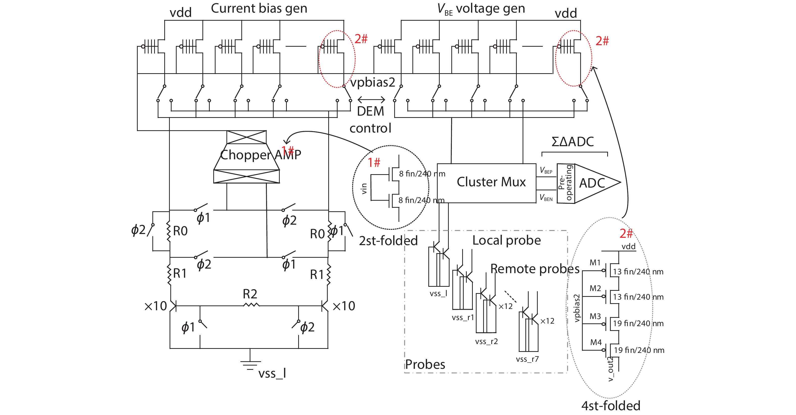
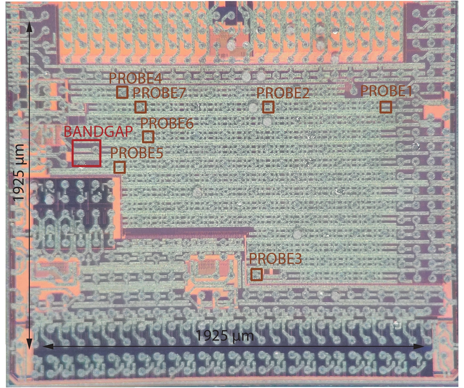
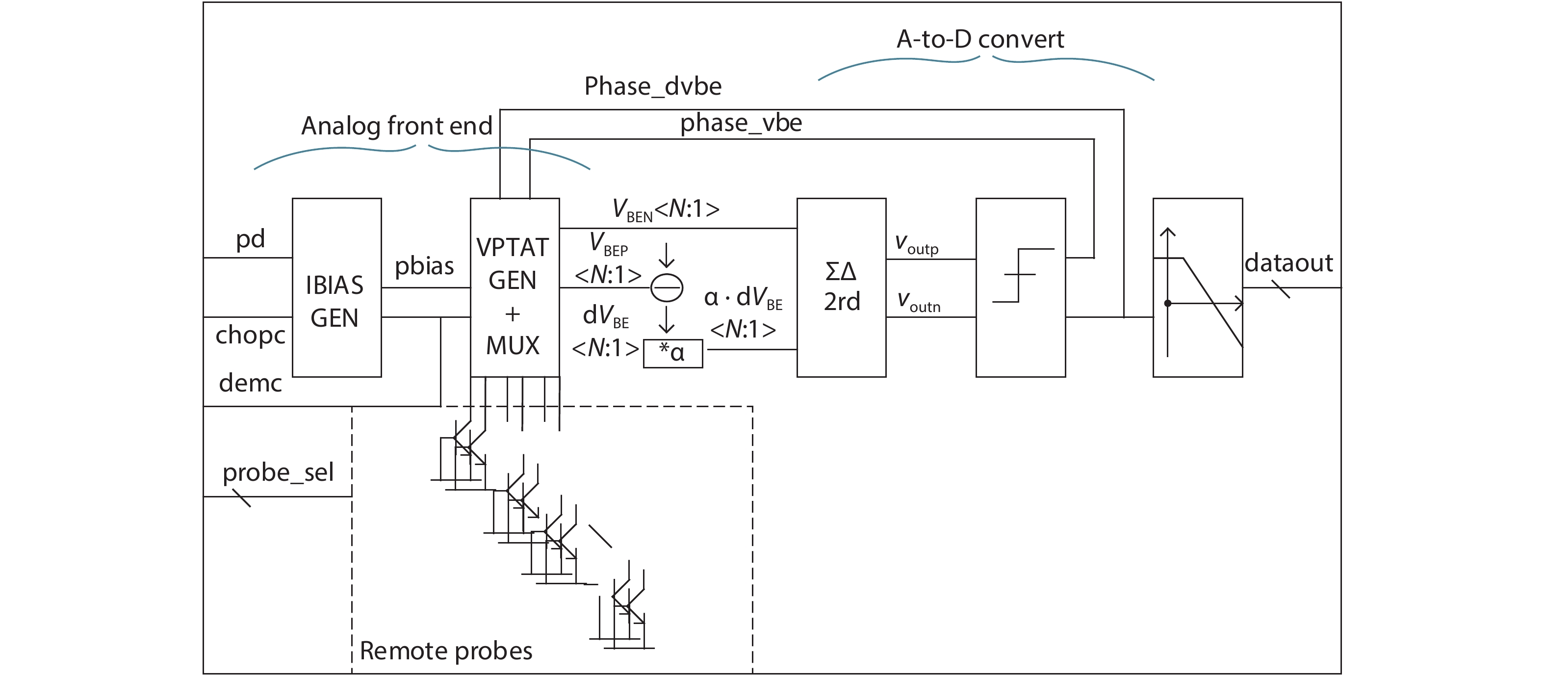
Abstract: This paper presents a 1.2 V high accuracy thermal sensor analog front-end circuit with 7 probes placed around the microprocessor chip. This analog front-end consists of a BGR (bandgap reference), a DEM (dynamic element matching) control, and probes. The BGR generates the voltages linear changed with temperature, which are followed by the data read out circuits. The superior accuracy of the BGR’s output voltage is a key factor for sensors fabricated via the FinFET digital process. Here, a 4-stage folded current bias structure is proposed, to increase DC accuracy and confer immunity against FinFET process variation due to limited device length and low current bias. At the same time, DEM is also adopted, so as to filter out current branch mismatches. Having been fabricated via a 12 nm FinFET CMOS process, 200 chips were tested. The measurement results demonstrate that these analog front-end circuits can work steadily below 1.2 V, and a less than 3.1% 3σ-accuracy level is achieved. Temperature stability is 0.088 mV/°C across a range from –40 to 130 °C.
Keywords: CMOS FinFET process, microprocessor, thermal sensor, BGR, 4-stage folded
| [1] |
Horng J J, Liu S L, Kundu A, et al. A 0.7 V resistive sensor with temperature/voltage detection function in 16 nm FinFET technologies. IEEE Symposium on VLSI Technology and Circuits, 2014, 54
|
| [2] |
Sönmez U, Sebastiano F, Makinwa K A A. 1650 μm2 thermal-diffusivity sensor with inaccuracies down to ±0.75 °C in 40nm CMOS. IEEE International Solid-State Circuits Conference, 2016, 206
|
| [3] |
Bakker A, Huijsing J. High-accuracy CMOS smart temperature sensors. Boston: Kluwer Academic, 2000
|
| [4] |
Meijer G C M, Wang G, Fruett F. Temperature sensors and voltage references implemented in CMOS technology. IEEE Sens J, 2001, 1(3), 225 doi: 10.1109/JSEN.2001.954835
|
| [5] |
Wang G, Heidari A, Makinwa K A A. An accurate BJT-based CMOS temperature sensor with duty-cycle-modulated output. IEEE Trans Ind Electron, 2017, 64, 1572 doi: 10.1109/TIE.2016.2614273
|
| [6] |
Ramirez J L, Tiol J P, Deotti D, et al. Delta-sigma modulated output temperature sensor for 1V voltage supply. IEEE Latin American Symposium on Circuits & Systems, 2019, 249
|
| [7] |
Ivanov V, Brederlow R, Gerber J. An ultra low power bandgap operational at supply from 0.75 V. IEEE J Solid-State Circuits, 2012, 47(7), 1515 doi: 10.1109/JSSC.2012.2191192
|
| [8] |
Lee J M, Ji Y, Choi S, et al. A 29nW bandgap reference circuit. IEEE International Solid-State Circuits Conference, 2015, 100
|
| [9] |
Ji Y, Jeon C, Son H, et al. A 9.3nW all-in-one bandgap voltage and current reference circuit. IEEE International Solid-State Circuits Conference, 2017, 100
|
| [10] |
Kamath U, Cullen E, Yu T, et al. A 1-V bandgap reference in 7-nm FinFET with a programmable temperature coefficient and inaccuracy of ±0.2% from –45 °C to 125 °C. IEEE J Solid-State Circuits, 2019, 54(7), 1830 doi: 10.1109/JSSC.2019.2919134
|
| [11] |
Meijer G C M. Thermal sensor based on transistors. Sens Actuators, 1986, 10(1), 103 doi: 10.1016/0250-6874(86)80037-3
|
| [12] |
Pertijs M A P, Niederkorn A, Ma X, et al. A CMOS smart temperature sensor with a 3σ inaccuracy of ±0.5 °C from –50 °C to 120 °C. IEEE J Solid-State Circuits, 2005, 40(2), 454 doi: 10.1109/JSSC.2004.841013
|
| [13] |
Yin L X, Du G, Liu X Y. Impact of ambient temperature on the self-heating effects in FinFETs. J Semicond, 2018, 39(9), 094011 doi: 10.1088/1674-4926/39/9/094011
|
| [14] |
Bakker A, Thiele K, Huijsing J. A CMOS nested chopper instrumentation amplifier with 100nV offset. IEEE International Solid-State Circuits Conference, 2000, 156
|
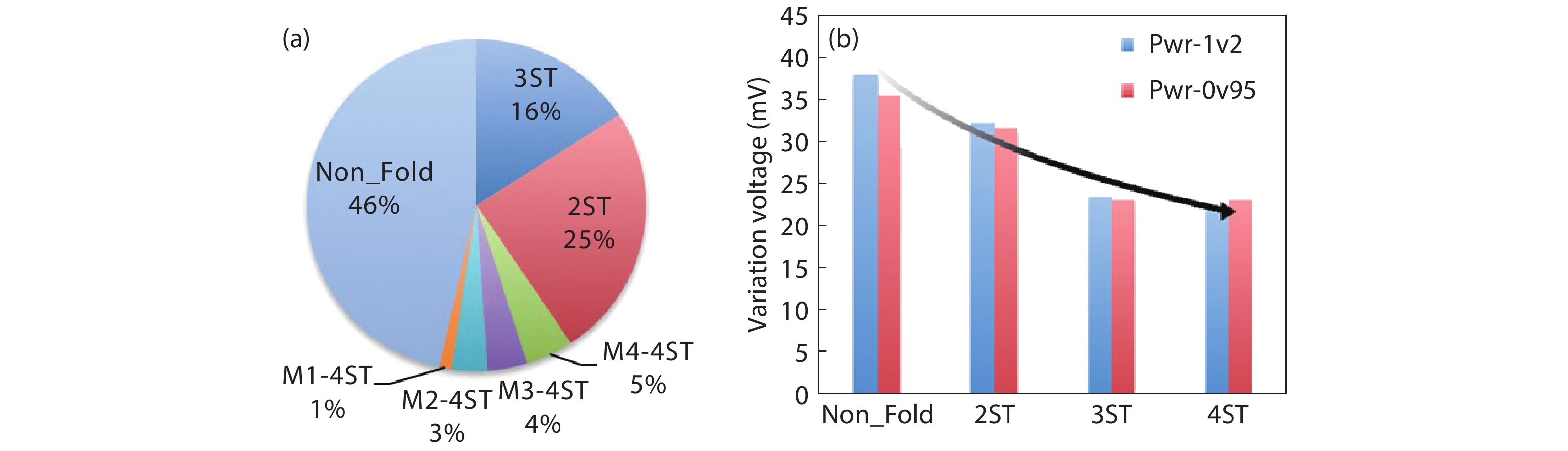
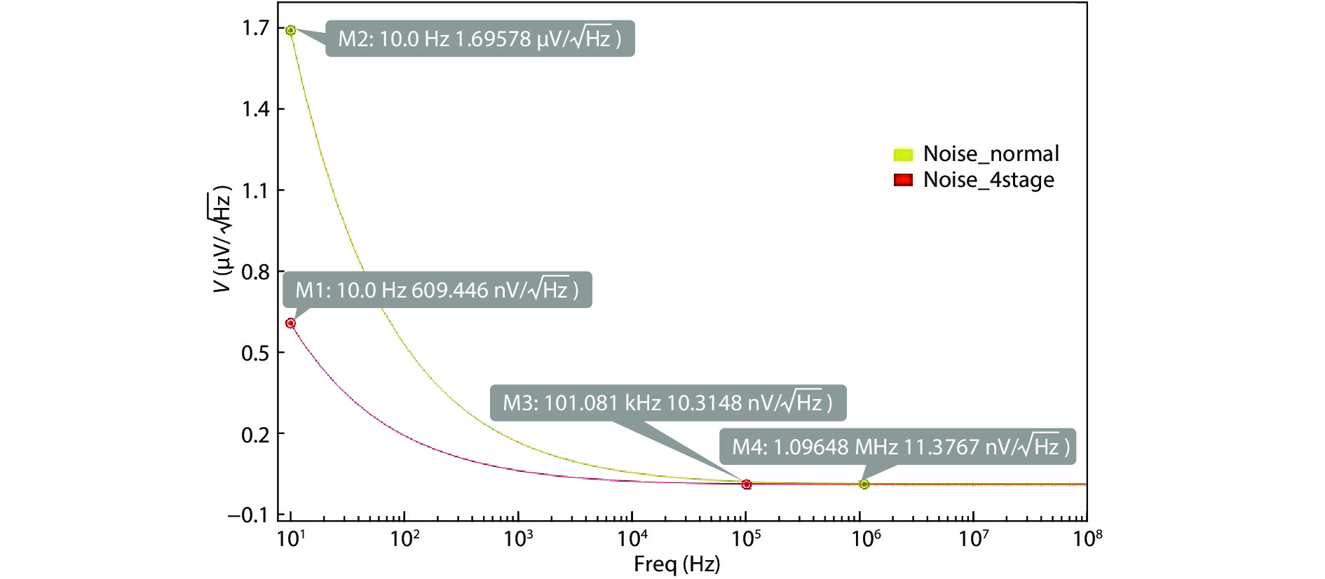
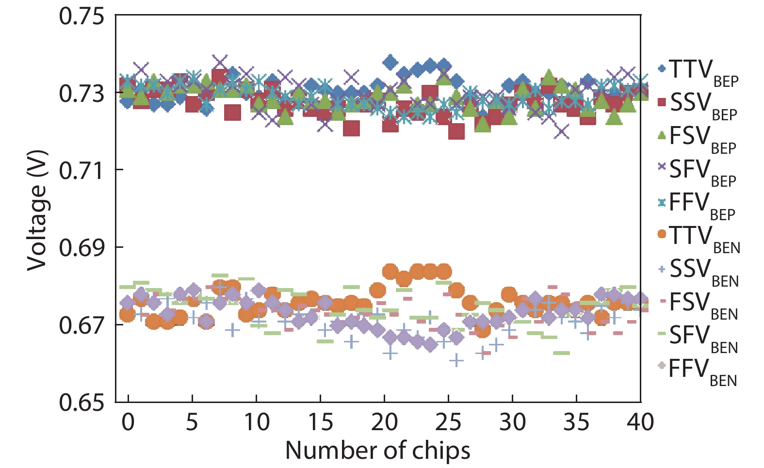
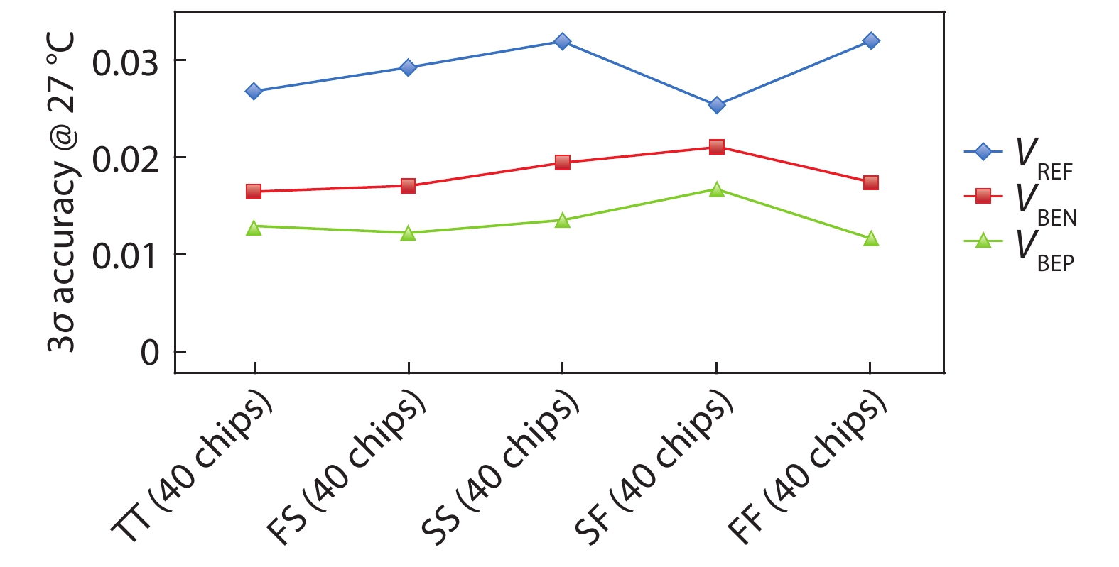
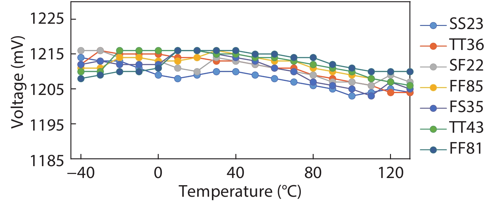
Table 1. Comparison table.
| Parameter | Ref. [7] | Ref. [8] | Ref. [9] | Ref. [10] | This work |
| Technology | 130 nm CMOS | 350 nm CMOS | 180 nm CMOS | 7 nm CMOS | 12 nm CMOS |
| Supply (V) | 0.75 | 1.2 | 1.2 | 1.375 | 1.2 |
| Temprange (°C) | –20 to 85 | –10 to 110 | 0 to 110 | –45 to 125 | –40 to 130 |
| 3σ (%) | 3 | 0.6 | 1.29 | 0.6 | <3.1 |
| TC (ppm) | 40 | 12.75 | 26 | 6 | 88 |
| Of chips | 90000 | 10 | 10 | 7 | 7/200 |
| BJT only | Yes | No | No | Yes | No |
| Type | SwitchCap | DC | DC | DC | DC |
| Power (nW) | 170 | 28.7 | 9.3 | 9.74 × 10⁵ | 4.96 × 10⁴ |
| Area (mm2) | 0.07 | 0.48 | 0.055 | 0.078 | 0.0124 |
 DownLoad: CSV
| [1] |
Horng J J, Liu S L, Kundu A, et al. A 0.7 V resistive sensor with temperature/voltage detection function in 16 nm FinFET technologies. IEEE Symposium on VLSI Technology and Circuits, 2014, 54
|
| [2] |
Sönmez U, Sebastiano F, Makinwa K A A. 1650 μm2 thermal-diffusivity sensor with inaccuracies down to ±0.75 °C in 40nm CMOS. IEEE International Solid-State Circuits Conference, 2016, 206
|
| [3] |
Bakker A, Huijsing J. High-accuracy CMOS smart temperature sensors. Boston: Kluwer Academic, 2000
|
| [4] |
Meijer G C M, Wang G, Fruett F. Temperature sensors and voltage references implemented in CMOS technology. IEEE Sens J, 2001, 1(3), 225 doi: 10.1109/JSEN.2001.954835
|
| [5] |
Wang G, Heidari A, Makinwa K A A. An accurate BJT-based CMOS temperature sensor with duty-cycle-modulated output. IEEE Trans Ind Electron, 2017, 64, 1572 doi: 10.1109/TIE.2016.2614273
|
| [6] |
Ramirez J L, Tiol J P, Deotti D, et al. Delta-sigma modulated output temperature sensor for 1V voltage supply. IEEE Latin American Symposium on Circuits & Systems, 2019, 249
|
| [7] |
Ivanov V, Brederlow R, Gerber J. An ultra low power bandgap operational at supply from 0.75 V. IEEE J Solid-State Circuits, 2012, 47(7), 1515 doi: 10.1109/JSSC.2012.2191192
|
| [8] |
Lee J M, Ji Y, Choi S, et al. A 29nW bandgap reference circuit. IEEE International Solid-State Circuits Conference, 2015, 100
|
| [9] |
Ji Y, Jeon C, Son H, et al. A 9.3nW all-in-one bandgap voltage and current reference circuit. IEEE International Solid-State Circuits Conference, 2017, 100
|
| [10] |
Kamath U, Cullen E, Yu T, et al. A 1-V bandgap reference in 7-nm FinFET with a programmable temperature coefficient and inaccuracy of ±0.2% from –45 °C to 125 °C. IEEE J Solid-State Circuits, 2019, 54(7), 1830 doi: 10.1109/JSSC.2019.2919134
|
| [11] |
Meijer G C M. Thermal sensor based on transistors. Sens Actuators, 1986, 10(1), 103 doi: 10.1016/0250-6874(86)80037-3
|
| [12] |
Pertijs M A P, Niederkorn A, Ma X, et al. A CMOS smart temperature sensor with a 3σ inaccuracy of ±0.5 °C from –50 °C to 120 °C. IEEE J Solid-State Circuits, 2005, 40(2), 454 doi: 10.1109/JSSC.2004.841013
|
| [13] |
Yin L X, Du G, Liu X Y. Impact of ambient temperature on the self-heating effects in FinFETs. J Semicond, 2018, 39(9), 094011 doi: 10.1088/1674-4926/39/9/094011
|
| [14] |
Bakker A, Thiele K, Huijsing J. A CMOS nested chopper instrumentation amplifier with 100nV offset. IEEE International Solid-State Circuits Conference, 2000, 156
|


Article views: 5110 Times PDF downloads: 137 Times Cited by: 0 Times
Received: 23 July 2020 Revised: 31 August 2020 Online: Accepted Manuscript: 20 October 2020Uncorrected proof: 23 October 2020Published: 10 March 2021
| Citation: |
Liqiong Yang, Linfeng Wang, Junhua Xiao, Longbing Zhang, Jian Wang. A 1.2 V, 3.1% 3σ-accuracy thermal sensor analog front-end circuit in 12 nm CMOS process[J]. Journal of Semiconductors, 2021, 42(3): 032401. doi: 10.1088/1674-4926/42/3/032401
****
L Q Yang, L F Wang, J H Xiao, L B Zhang, J Wang, A 1.2 V, 3.1% 3σ-accuracy thermal sensor analog front-end circuit in 12 nm CMOS process[J]. J. Semicond., 2021, 42(3): 032401. doi: 10.1088/1674-4926/42/3/032401.

|
| [1] |
Horng J J, Liu S L, Kundu A, et al. A 0.7 V resistive sensor with temperature/voltage detection function in 16 nm FinFET technologies. IEEE Symposium on VLSI Technology and Circuits, 2014, 54
|
| [2] |
Sönmez U, Sebastiano F, Makinwa K A A. 1650 μm2 thermal-diffusivity sensor with inaccuracies down to ±0.75 °C in 40nm CMOS. IEEE International Solid-State Circuits Conference, 2016, 206
|
| [3] |
Bakker A, Huijsing J. High-accuracy CMOS smart temperature sensors. Boston: Kluwer Academic, 2000
|
| [4] |
Meijer G C M, Wang G, Fruett F. Temperature sensors and voltage references implemented in CMOS technology. IEEE Sens J, 2001, 1(3), 225 doi: 10.1109/JSEN.2001.954835
|
| [5] |
Wang G, Heidari A, Makinwa K A A. An accurate BJT-based CMOS temperature sensor with duty-cycle-modulated output. IEEE Trans Ind Electron, 2017, 64, 1572 doi: 10.1109/TIE.2016.2614273
|
| [6] |
Ramirez J L, Tiol J P, Deotti D, et al. Delta-sigma modulated output temperature sensor for 1V voltage supply. IEEE Latin American Symposium on Circuits & Systems, 2019, 249
|
| [7] |
Ivanov V, Brederlow R, Gerber J. An ultra low power bandgap operational at supply from 0.75 V. IEEE J Solid-State Circuits, 2012, 47(7), 1515 doi: 10.1109/JSSC.2012.2191192
|
| [8] |
Lee J M, Ji Y, Choi S, et al. A 29nW bandgap reference circuit. IEEE International Solid-State Circuits Conference, 2015, 100
|
| [9] |
Ji Y, Jeon C, Son H, et al. A 9.3nW all-in-one bandgap voltage and current reference circuit. IEEE International Solid-State Circuits Conference, 2017, 100
|
| [10] |
Kamath U, Cullen E, Yu T, et al. A 1-V bandgap reference in 7-nm FinFET with a programmable temperature coefficient and inaccuracy of ±0.2% from –45 °C to 125 °C. IEEE J Solid-State Circuits, 2019, 54(7), 1830 doi: 10.1109/JSSC.2019.2919134
|
| [11] |
Meijer G C M. Thermal sensor based on transistors. Sens Actuators, 1986, 10(1), 103 doi: 10.1016/0250-6874(86)80037-3
|
| [12] |
Pertijs M A P, Niederkorn A, Ma X, et al. A CMOS smart temperature sensor with a 3σ inaccuracy of ±0.5 °C from –50 °C to 120 °C. IEEE J Solid-State Circuits, 2005, 40(2), 454 doi: 10.1109/JSSC.2004.841013
|
| [13] |
Yin L X, Du G, Liu X Y. Impact of ambient temperature on the self-heating effects in FinFETs. J Semicond, 2018, 39(9), 094011 doi: 10.1088/1674-4926/39/9/094011
|
| [14] |
Bakker A, Thiele K, Huijsing J. A CMOS nested chopper instrumentation amplifier with 100nV offset. IEEE International Solid-State Circuits Conference, 2000, 156
|

 WeChat ID
Journal of Semiconductors © 2017 All Rights Reserved 京ICP备05085259号-2