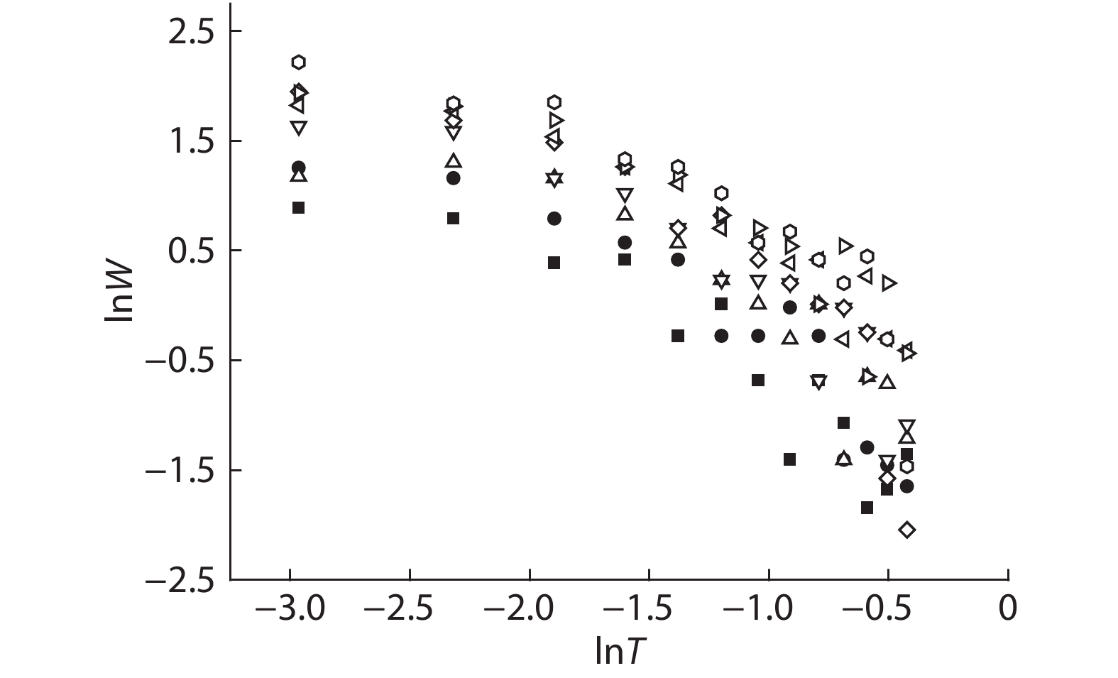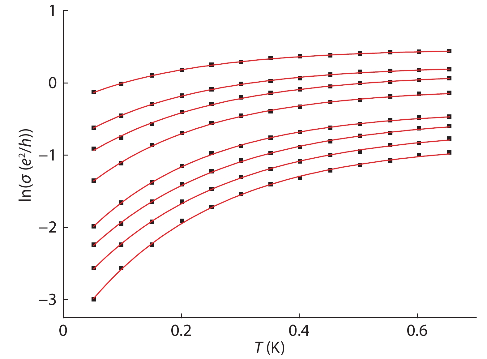
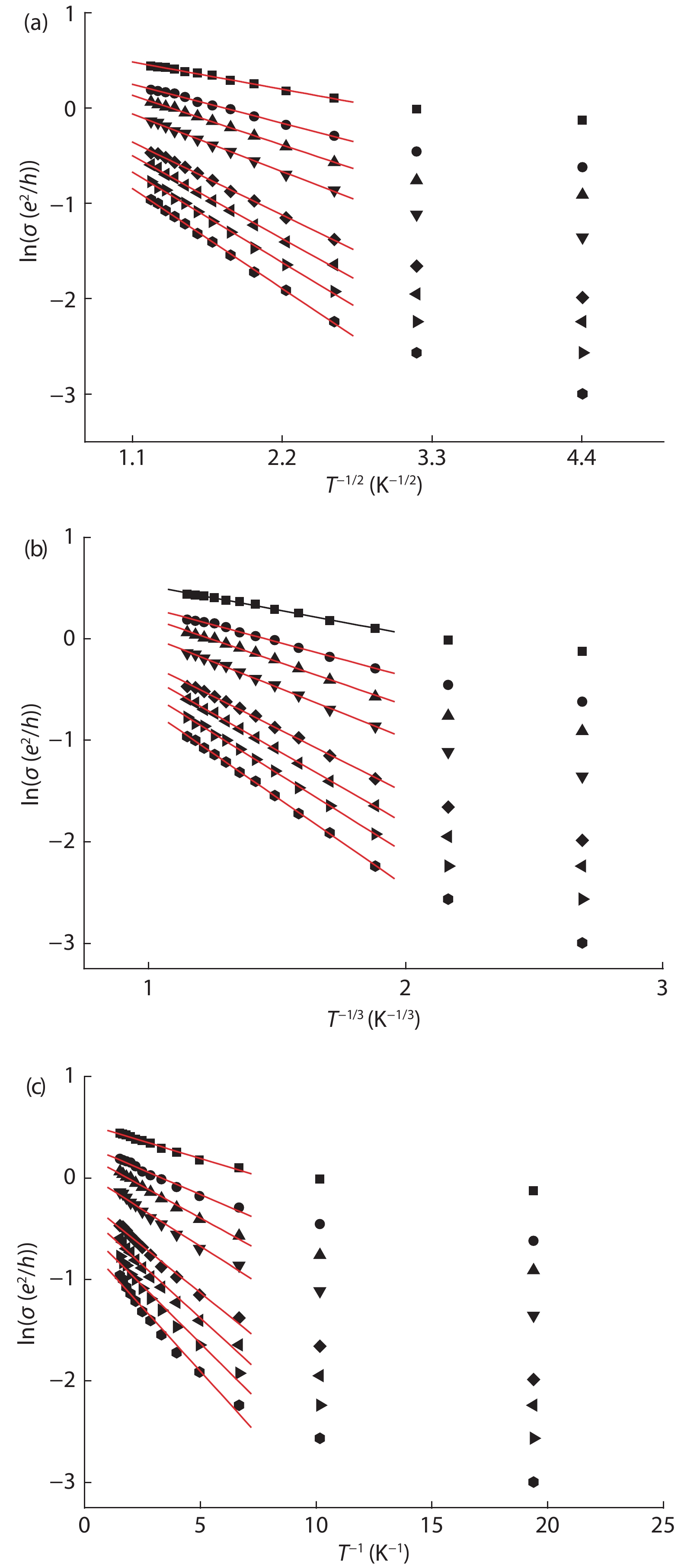
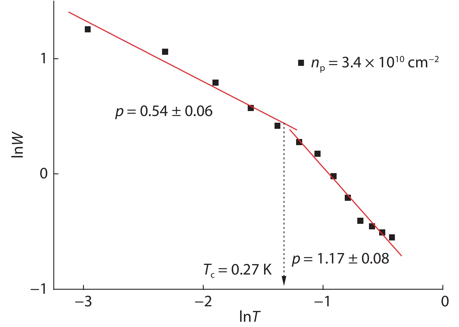
Fig. 1.
Adjustment of conductivity dependence of temperature for 2D p-GaAs system sample for different carrier densities.
ARTICLES
S. Dlimi1, , A. El kaaouachi1, 2, L. Limouny1 and B. A. Hammou2
Corresponding author: S. Dlimi, dlimi1975@gmail.com
Abstract: In this paper, we discuss low-temperature hopping-conductivity behavior in the insulating phase, in the absence of a magnetic field. We conduct a theoretical study of the crossover from hopping to activated transport in a GaAs two-dimensional hole system at low temperatures, finding that a crossover takes place from the Efros-Shklovskii variable-range hopping (VRH) regime to an activated regime in this system. This conductivity behavior in p-GaAs quantum wells is qualitatively consistent with the laws laid down in theories of localized electron interactions. Given sufficiently strong interactions, the holes in the localized states are able to hop collectively.
Keywords: quantum wells, 2D GaAs heterostructues, transport properties, variable range hopping
| [1] |
Mott N F. Conduction in glasses containing transition metal ions. J Non-Cryst Solids, 1968, 1, 1 doi: 10.1016/0022-3093(68)90002-1
|
| [2] |
Ferrus T, George R, Barnes C W, et al. Activation mechanisms in sodium-doped silicon MOSFETs. J Phys: Condens Matter, 2007, 19, 226216 doi: 10.1088/0953-8984/19/22/226216
|
| [3] |
Arshad M, Abushad M, Husain S, et al. Investigation of structural, optical and electrical transport properties of yttrium doped La0.7Ca0.3MnO3 perovskites. Electron Mater Lett, 2020, 16, 321 doi: 10.1007/s13391-020-00216-1
|
| [4] |
Dhankhar S, Kundu R S, Rani S, et al. Zinc chloride modified electronic transport and relaxation studies in barium-tellurite glasses. Electron Mater Lett, 2017, 13, 412 doi: 10.1007/s13391-017-6138-1
|
| [5] |
Bourim E M, Han J I. Electrical characterization and thermal admittance spectroscopy analysis of InGaN/GaN MQW blue LED structure. Electron Mater Lett, 2015, 11, 982 doi: 10.1007/s13391-015-5180-0
|
| [6] |
Dlimi S, Limouny L, Hemine J, et al. Efros–Shklovskii hopping in the electronic transport in 2D p-GaAs. Lith J Phys, 2020, 60, 167 doi: 10.3952/physics.v60i3.4303
|
| [7] |
Abrahams E, Anderson P W, Licciardello D C, et al. Scaling theory of localization: Absence of quantum diffusion in two dimensions. Phys Rev Lett, 1979, 42, 673 doi: 10.1103/PhysRevLett.42.673
|
| [8] |
Efros A L, Shklovskii B I. Coulomb gap and low temperature conductivity of disordered systems. J Phys C, 1975, 8, L49 doi: 10.1088/0022-3719/8/4/003
|
| [9] |
Ono Y, Morizur J F, Nishiguchi K, et al. Impurity conduction in phosphorus-doped buried-channel silicon-on-insulator field-effect transistors at temperatures between 10 and 295 K. Phys Rev B, 2006, 74, 235317 doi: 10.1103/PhysRevB.74.235317
|
| [10] |
Liu H, Pourret A, Guyot-Sionnest P. Mott and Efros-Shklovskii variable range hopping in CdSe quantum dots films. ACS Nano, 2010, 4, 5211 doi: 10.1021/nn101376u
|
| [11] |
Narjis A, El kaaouachi A, Limouny L, et al. Study of insulating electrical conductivity in hydrogenated amorphous silicon-nickel alloys at very low temperature. Physica B, 2011, 406, 4155 doi: 10.1016/j.physb.2011.08.021
|
| [12] |
Narjis A, Biskupski G, Daoudi E, et al. Low temperature electrical resistivity of polycrystalline La0.67Sr0.33MnO3 thin films. Mater Sci Semicond Process, 2013, 16, 1257 doi: 10.1016/j.mssp.2013.01.004
|
| [13] |
Shklovskii B I, Efros A L. Percolation theory. In: Electronic Properties of Doped Semiconductors. Berlin, Heidelberg: Springer Berlin Heidelberg, 1984, 94
|
| [14] |
van Keuls F W, Hu X L, Jiang H W, et al. Screening of the Coulomb interaction in two-dimensional variable-range hopping. Phys Rev B, 1997, 56, 1161 doi: 10.1103/PhysRevB.56.1161
|
| [15] |
Dlimi S, El Kaaouachi A, Narjis A, et al. Evidence for the correlated hopping mechanism in p-GaAs near the 2D MIT at B = 0 T. J Optoelectron Adv Mater, 2013, 15, 1222
|
| [16] |
Briggs A, Guldner Y, Vieren J P, et al. Low-temperature investigations of the quantum Hall effect in InxGa1– xAs–InP heterojunctions. Phys Rev B, 1983, 27, 6549 doi: 10.1103/PhysRevB.27.6549
|
| [17] |
Hamilton A R, Simmons M Y, Pepper M, et al. Localisation and the metal-insulator transition in two dimensions. Physica B, 2001, 296, 21 doi: 10.1016/S0921-4526(00)00773-0
|
| [18] |
Minkov G M, Germanenko A V, Gornyi I V. Magnetoresistance and dephasing in a two-dimensional electron gas at intermediate conductances. Phys Rev B, 2004, 70, 245423 doi: 10.1103/PhysRevB.70.245423
|
| [19] |
Lee Y C, Liu C I, Yang Y F, et al. Crossover from Efros-Shklovskii to Mott variable range hopping in monolayer epitaxial graphene grown on SiC. Chin J Phys, 2017, 55, 1235 doi: 10.1016/j.cjph.2017.06.007
|
| [20] |
Kim J J, Lee H J. Observation of a nonmagnetic hard gap in amorphous In/InO x films in the hopping regime. Phys Rev Lett, 1993, 70, 2798 doi: 10.1103/PhysRevLett.70.2798
|
| [21] |
Chauve P, Giamarchi T, Le Doussal P. Creep and depinning in disordered media. Phys Rev B, 2000, 62, 6241 doi: 10.1103/PhysRevB.62.6241
|
| [22] |
Shashkin A A, Dolgopolov V T, Kravchenko G V, et al. Percolation metal-insulator transitions in the two-dimensional electron system of AlGaAs/GaAs heterostructures. Phys Rev Lett, 1994, 73, 3141 doi: 10.1103/PhysRevLett.73.3141
|
| [23] |
Arapov Y G, Gudina S V, Klepikova A S, et al. Quantum Hall plateau-plateau transitions in n-InGaAs/GaAs heterostructures before and after IR illumination. Low Temp Phys, 2015, 41, 106 doi: 10.1063/1.4908192
|
| [24] |
Das Sarma S, Lilly M P, Hwang E H, et al. Two-dimensional metal-insulator transition as a percolation transition in a high-mobility electron system. Phys Rev Lett, 2005, 94, 136401 doi: 10.1103/PhysRevLett.94.136401
|
| [25] |
Dlimi S, El kaaouachi A, Narjis A. Density inhomogeneity driven metal-insulator transition in 2D p-GaAs. Phys E, 2013, 54, 181 doi: 10.1016/j.physe.2013.07.001
|
| [26] |
van Keuls F W, Hu X L, Dahm A J, et al. The Coulomb gap and the transition to Mott hopping. Surf Sci, 1996, 361/362, 945 doi: 10.1016/0039-6028(96)00570-5
|
| [27] |
Du L J, Li X W, Lou W K, et al. Evidence for a topological excitonic insulator in InAs/GaSb bilayers. Nat Commun, 2017, 8, 1971 doi: 10.1038/s41467-017-01988-1
|
| [28] |
Jiang Z Y, Lou W K, Liu Y, et al. Spin-triplet excitonic insulator: The case of semihydrogenated graphene. Phys Rev Lett, 2020, 124, 166401 doi: 10.1103/PhysRevLett.124.166401
|
| [29] |
Mason W, Kravchenko S V, Bowker G E, et al. Experimental evidence for a Coulomb gap in two dimensions. Phys Rev B, 1995, 52, 7857 doi: 10.1103/PhysRevB.52.7857
|
| [30] |
Dlimi S, El kaaouachi A, Narjis A, et al. Hopping energy and percolation-type transport in p-GaAs low densities near the 2D metal-insulator transition at zero magnetic field. J Phys Chem Solids, 2013, 74, 1349 doi: 10.1016/j.jpcs.2013.05.004
|
| [31] |
Khondaker S I, Shlimak I S, Nicholls J T, et al. Two-dimensional hopping conductivity in a δ-doped GaAs/AlxGa1– xAs heterostructure. Phys Rev B, 1999, 59, 4580 doi: 10.1103/PhysRevB.59.4580
|


Article views: 4283 Times PDF downloads: 104 Times Cited by: 0 Times
Received: 01 September 2020 Revised: 16 September 2020 Online: Accepted Manuscript: 22 October 2020Uncorrected proof: 26 October 2020Published: 01 May 2021
| Citation: |
S. Dlimi, A. El kaaouachi, L. Limouny, B. A. Hammou. A crossover from Efros–Shklovskii hopping to activated transport in a GaAs two-dimensional hole system at low temperatures[J]. Journal of Semiconductors, 2021, 42(5): 052001. doi: 10.1088/1674-4926/42/5/052001
****
S Dlimi, A El kaaouachi, L Limouny, B A Hammou, A crossover from Efros–Shklovskii hopping to activated transport in a GaAs two-dimensional hole system at low temperatures[J]. J. Semicond., 2021, 42(5): 052001. doi: 10.1088/1674-4926/42/5/052001.

|
| [1] |
Mott N F. Conduction in glasses containing transition metal ions. J Non-Cryst Solids, 1968, 1, 1 doi: 10.1016/0022-3093(68)90002-1
|
| [2] |
Ferrus T, George R, Barnes C W, et al. Activation mechanisms in sodium-doped silicon MOSFETs. J Phys: Condens Matter, 2007, 19, 226216 doi: 10.1088/0953-8984/19/22/226216
|
| [3] |
Arshad M, Abushad M, Husain S, et al. Investigation of structural, optical and electrical transport properties of yttrium doped La0.7Ca0.3MnO3 perovskites. Electron Mater Lett, 2020, 16, 321 doi: 10.1007/s13391-020-00216-1
|
| [4] |
Dhankhar S, Kundu R S, Rani S, et al. Zinc chloride modified electronic transport and relaxation studies in barium-tellurite glasses. Electron Mater Lett, 2017, 13, 412 doi: 10.1007/s13391-017-6138-1
|
| [5] |
Bourim E M, Han J I. Electrical characterization and thermal admittance spectroscopy analysis of InGaN/GaN MQW blue LED structure. Electron Mater Lett, 2015, 11, 982 doi: 10.1007/s13391-015-5180-0
|
| [6] |
Dlimi S, Limouny L, Hemine J, et al. Efros–Shklovskii hopping in the electronic transport in 2D p-GaAs. Lith J Phys, 2020, 60, 167 doi: 10.3952/physics.v60i3.4303
|
| [7] |
Abrahams E, Anderson P W, Licciardello D C, et al. Scaling theory of localization: Absence of quantum diffusion in two dimensions. Phys Rev Lett, 1979, 42, 673 doi: 10.1103/PhysRevLett.42.673
|
| [8] |
Efros A L, Shklovskii B I. Coulomb gap and low temperature conductivity of disordered systems. J Phys C, 1975, 8, L49 doi: 10.1088/0022-3719/8/4/003
|
| [9] |
Ono Y, Morizur J F, Nishiguchi K, et al. Impurity conduction in phosphorus-doped buried-channel silicon-on-insulator field-effect transistors at temperatures between 10 and 295 K. Phys Rev B, 2006, 74, 235317 doi: 10.1103/PhysRevB.74.235317
|
| [10] |
Liu H, Pourret A, Guyot-Sionnest P. Mott and Efros-Shklovskii variable range hopping in CdSe quantum dots films. ACS Nano, 2010, 4, 5211 doi: 10.1021/nn101376u
|
| [11] |
Narjis A, El kaaouachi A, Limouny L, et al. Study of insulating electrical conductivity in hydrogenated amorphous silicon-nickel alloys at very low temperature. Physica B, 2011, 406, 4155 doi: 10.1016/j.physb.2011.08.021
|
| [12] |
Narjis A, Biskupski G, Daoudi E, et al. Low temperature electrical resistivity of polycrystalline La0.67Sr0.33MnO3 thin films. Mater Sci Semicond Process, 2013, 16, 1257 doi: 10.1016/j.mssp.2013.01.004
|
| [13] |
Shklovskii B I, Efros A L. Percolation theory. In: Electronic Properties of Doped Semiconductors. Berlin, Heidelberg: Springer Berlin Heidelberg, 1984, 94
|
| [14] |
van Keuls F W, Hu X L, Jiang H W, et al. Screening of the Coulomb interaction in two-dimensional variable-range hopping. Phys Rev B, 1997, 56, 1161 doi: 10.1103/PhysRevB.56.1161
|
| [15] |
Dlimi S, El Kaaouachi A, Narjis A, et al. Evidence for the correlated hopping mechanism in p-GaAs near the 2D MIT at B = 0 T. J Optoelectron Adv Mater, 2013, 15, 1222
|
| [16] |
Briggs A, Guldner Y, Vieren J P, et al. Low-temperature investigations of the quantum Hall effect in InxGa1– xAs–InP heterojunctions. Phys Rev B, 1983, 27, 6549 doi: 10.1103/PhysRevB.27.6549
|
| [17] |
Hamilton A R, Simmons M Y, Pepper M, et al. Localisation and the metal-insulator transition in two dimensions. Physica B, 2001, 296, 21 doi: 10.1016/S0921-4526(00)00773-0
|
| [18] |
Minkov G M, Germanenko A V, Gornyi I V. Magnetoresistance and dephasing in a two-dimensional electron gas at intermediate conductances. Phys Rev B, 2004, 70, 245423 doi: 10.1103/PhysRevB.70.245423
|
| [19] |
Lee Y C, Liu C I, Yang Y F, et al. Crossover from Efros-Shklovskii to Mott variable range hopping in monolayer epitaxial graphene grown on SiC. Chin J Phys, 2017, 55, 1235 doi: 10.1016/j.cjph.2017.06.007
|
| [20] |
Kim J J, Lee H J. Observation of a nonmagnetic hard gap in amorphous In/InO x films in the hopping regime. Phys Rev Lett, 1993, 70, 2798 doi: 10.1103/PhysRevLett.70.2798
|
| [21] |
Chauve P, Giamarchi T, Le Doussal P. Creep and depinning in disordered media. Phys Rev B, 2000, 62, 6241 doi: 10.1103/PhysRevB.62.6241
|
| [22] |
Shashkin A A, Dolgopolov V T, Kravchenko G V, et al. Percolation metal-insulator transitions in the two-dimensional electron system of AlGaAs/GaAs heterostructures. Phys Rev Lett, 1994, 73, 3141 doi: 10.1103/PhysRevLett.73.3141
|
| [23] |
Arapov Y G, Gudina S V, Klepikova A S, et al. Quantum Hall plateau-plateau transitions in n-InGaAs/GaAs heterostructures before and after IR illumination. Low Temp Phys, 2015, 41, 106 doi: 10.1063/1.4908192
|
| [24] |
Das Sarma S, Lilly M P, Hwang E H, et al. Two-dimensional metal-insulator transition as a percolation transition in a high-mobility electron system. Phys Rev Lett, 2005, 94, 136401 doi: 10.1103/PhysRevLett.94.136401
|
| [25] |
Dlimi S, El kaaouachi A, Narjis A. Density inhomogeneity driven metal-insulator transition in 2D p-GaAs. Phys E, 2013, 54, 181 doi: 10.1016/j.physe.2013.07.001
|
| [26] |
van Keuls F W, Hu X L, Dahm A J, et al. The Coulomb gap and the transition to Mott hopping. Surf Sci, 1996, 361/362, 945 doi: 10.1016/0039-6028(96)00570-5
|
| [27] |
Du L J, Li X W, Lou W K, et al. Evidence for a topological excitonic insulator in InAs/GaSb bilayers. Nat Commun, 2017, 8, 1971 doi: 10.1038/s41467-017-01988-1
|
| [28] |
Jiang Z Y, Lou W K, Liu Y, et al. Spin-triplet excitonic insulator: The case of semihydrogenated graphene. Phys Rev Lett, 2020, 124, 166401 doi: 10.1103/PhysRevLett.124.166401
|
| [29] |
Mason W, Kravchenko S V, Bowker G E, et al. Experimental evidence for a Coulomb gap in two dimensions. Phys Rev B, 1995, 52, 7857 doi: 10.1103/PhysRevB.52.7857
|
| [30] |
Dlimi S, El kaaouachi A, Narjis A, et al. Hopping energy and percolation-type transport in p-GaAs low densities near the 2D metal-insulator transition at zero magnetic field. J Phys Chem Solids, 2013, 74, 1349 doi: 10.1016/j.jpcs.2013.05.004
|
| [31] |
Khondaker S I, Shlimak I S, Nicholls J T, et al. Two-dimensional hopping conductivity in a δ-doped GaAs/AlxGa1– xAs heterostructure. Phys Rev B, 1999, 59, 4580 doi: 10.1103/PhysRevB.59.4580
|

 WeChat ID
Journal of Semiconductors © 2017 All Rights Reserved 京ICP备05085259号-2

 DownLoad: