


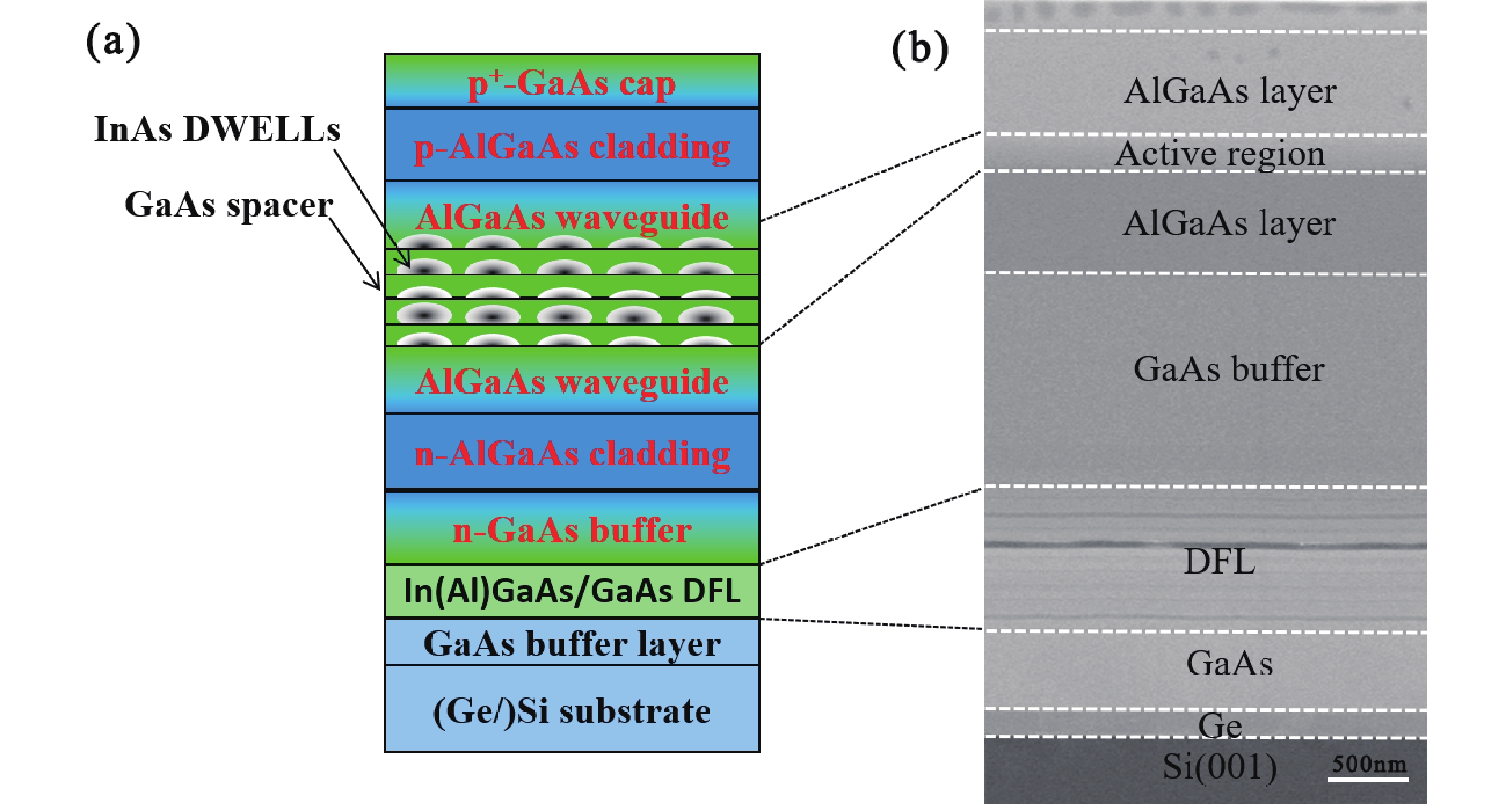
Fig. 1.
(Color online) (a) Schematic of the QD laser structure grown on silicon substrates, and (b) the corresponding cross-sectional SEM image.
ARTICLES
Tianyi Tang1, 2, 3, Tian Yu1, 2, 3, Guanqing Yang1, 2, 3, Jiaqian Sun1, 2, 3, Wenkang Zhan1, 2, 3, Bo Xu1, 2, 3, , Chao Zhao1, 2, 3, and Zhanguo Wang1, 2, 3
Corresponding author: Bo Xu, srex@semi.ac.cn; Chao Zhao, zhaochao@semi.ac.cn
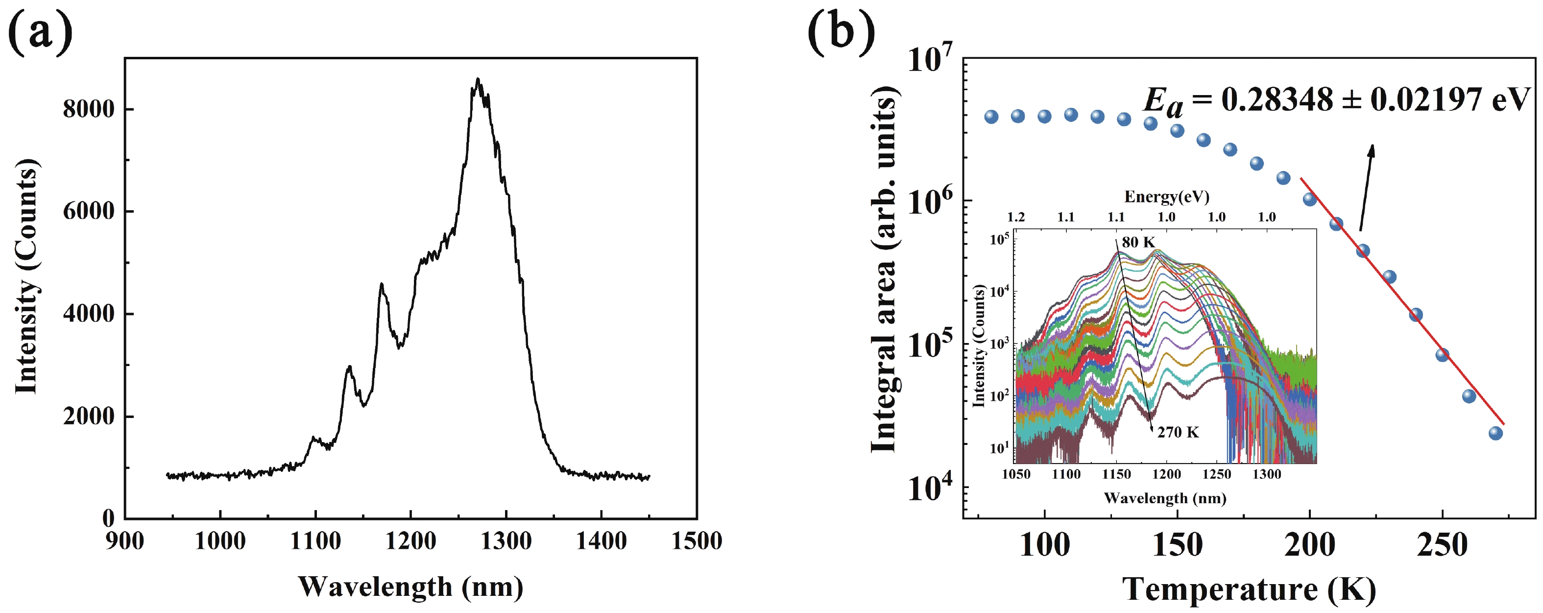
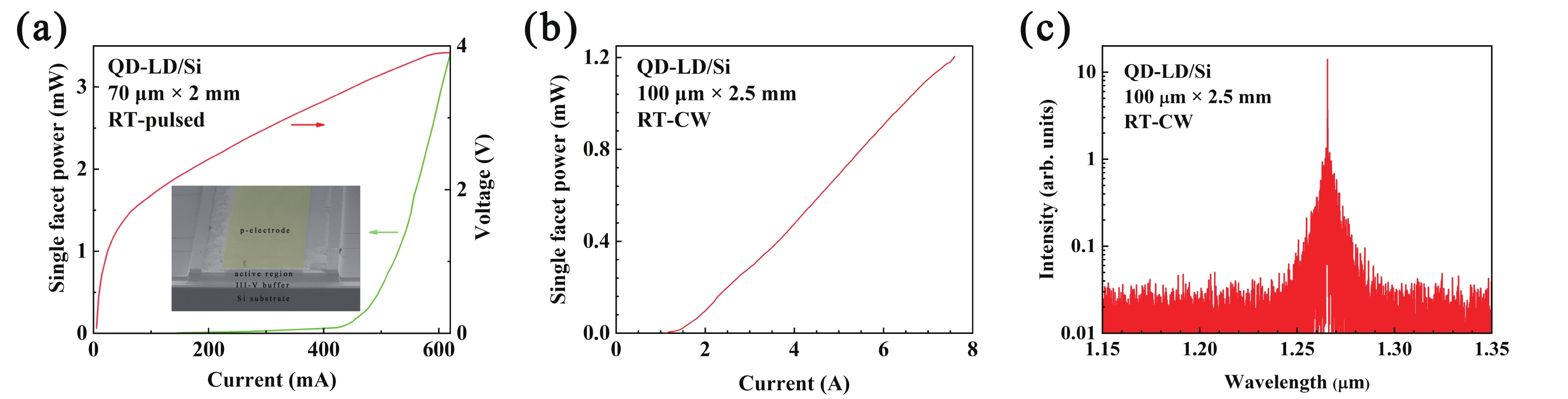
Abstract: InAs/GaAs quantum dot (QD) lasers were grown on silicon substrates using a thin Ge buffer and three-step growth method in the molecular beam epitaxy (MBE) system. In addition, strained superlattices were used to prevent threading dislocations from propagating to the active region of the laser. The as-grown material quality was characterized by the transmission electron microscope, scanning electron microscope, X-ray diffraction, atomic force microscope, and photoluminescence spectroscopy. The results show that a high-quality GaAs buffer with few dislocations was obtained by the growth scheme we developed. A broad-area edge-emitting laser was also fabricated. The O-band laser exhibited a threshold current density of 540 A/cm2 at room temperature under continuous wave conditions. This work demonstrates the potential of large-scale and low-cost manufacturing of the O-band InAs/GaAs quantum dot lasers on silicon substrates.
Keywords: semiconductor laser, molecular beam epitaxy, quantum dots, III–V on Si, silicon photonics
| [1] |
Won R. Integrating silicon photonics. Nat Photonics, 2010, 4, 498 doi: 10.1038/nphoton.2010.189
|
| [2] |
Miller D. Device requirements for optical interconnects to silicon chips. Proc IEEE, 2009, 97, 1166 doi: 10.1109/JPROC.2009.2014298
|
| [3] |
Zhou Z, Chen R, Li X, et al. Development trends in silicon photonics for data centers. Opt Fiber Technol, 2018, 44, 13 doi: 10.1016/j.yofte.2018.03.009
|
| [4] |
Rickman A. The commercialization of silicon photonics. Nat Photonics, 2014, 8, 579 doi: 10.1038/nphoton.2014.175
|
| [5] |
Liang D, Bowers J E. Recent progress in lasers on silicon. Nat Photonics, 2010, 4, 511 doi: 10.1038/nphoton.2010.167
|
| [6] |
Wirths S, Geiger R, von den Driesch N, et al. Lasing in direct-bandgap GeSn alloy grown on Si. Nat Photonics, 2015, 9, 88 doi: 10.1038/nphoton.2014.321
|
| [7] |
Tang M, Park J S, Wang Z, et al. Integration of III–V lasers on Si for Si photonics. Prog Quantum Electron, 2019, 66, 1 doi: 10.1016/j.pquantelec.2019.05.002
|
| [8] |
Wang J, Ren X, Deng C, et al. Extremely low-threshold current density InGaAs/AlGaAs quantum-well lasers on silicon. J Lightwave Technol, 2015, 33, 3163 doi: 10.1109/JLT.2015.2438873
|
| [9] |
Rio Calvo M, Monge Bartolomé L, Bahriz M, et al. Mid-infrared laser diodes epitaxially grown on on-axis (001) silicon. Optica, 2020, 7, 263 doi: 10.1364/OPTICA.388383
|
| [10] |
Wang Z, Van Gasse K, Moskalenko V, et al. A III–V-on-Si ultra-dense comb laser. Light Sci Appl, 2017, 6, e16260 doi: 10.1038/lsa.2016.260
|
| [11] |
Billah M R, Blaicher M, Hoose T, et al. Hybrid integration of silicon photonics circuits and InP lasers by photonic wire bonding. Optica, 2018, 5, 876 doi: 10.1364/OPTICA.5.000876
|
| [12] |
Jang B, Tanabe K, Kako S, et al. A hybrid silicon evanescent quantum dot laser. Appl Phys Express, 2016, 9, 092102 doi: 10.7567/APEX.9.092102
|
| [13] |
Jhang Y H, Mochida R, Tanabe K, et al. Direct modulation of 1.3 μm quantum dot lasers on silicon at 60 °C. Opt Express, 2016, 24, 18428 doi: 10.1109/ICIPRM.2016.7528534
|
| [14] |
Chen S, Li W, Wu J, et al. Electrically pumped continuous-wave III–V quantum dot lasers on silicon. Nat Photonics, 2016, 10, 307 doi: 10.1038/nphoton.2016.21
|
| [15] |
Liao M, Chen S, Park J S, et al. III–V quantum-dot lasers monolithically grown on silicon. Semicond Sci Technol, 2018, 33, 123002 doi: 10.1088/1361-6641/aae6a5
|
| [16] |
Park J S, Tang M, Chen S, et al. Heteroepitaxial growth of III–V semiconductors on silicon. Crystals, 2020, 10, 1163 doi: 10.3390/cryst10121163
|
| [17] |
Matthews J W, Blakeslee A E. Defects in epitaxial multilayers. J Cryst Growth, 1974, 27, 118 doi: 10.1016/S0022-0248(74)80055-2
|
| [18] |
Li Q, Lau K M. Epitaxial growth of highly mismatched III–V materials on (001) silicon for electronics and optoelectronics. Prog Cryst Growth Charact Mater, 2017, 63, 105 doi: 10.1016/j.pcrysgrow.2017.10.001
|
| [19] |
Georgakilas A, Stoemenos J, Tsagaraki K, et al. Generation and annihilation of antiphase domain boundaries in GaAs on Si grown by molecular beam epitaxy. J Mater Res, 1993, 8, 1908 doi: 10.1557/JMR.1993.1908
|
| [20] |
Kroemer H. Polar-on-nonpolar epitaxy. J Cryst Growth, 1987, 81, 193 doi: 10.1016/0022-0248(87)90391-5
|
| [21] |
Ye T, Suo Z, Evans A G. Thin film cracking and the roles of substrate and interface. Int J Solids Struct, 1992, 29, 2639 doi: 10.1016/0020-7683(92)90227-K
|
| [22] |
Wei W, Feng Q, Wang Z, et al. Perspective: optically-pumped III–V quantum dot microcavity lasers via CMOS compatible patterned Si (001) substrates. J Semicond, 2019, 40, 101303 doi: 10.1088/1674-4926/40/10/101303
|
| [23] |
Ward T, Sánchez A M, Tang M, et al. Design rules for dislocation filters. J Appl Phys, 2014, 116, 063508 doi: 10.1063/1.4892162
|
| [24] |
Beanland R, Sánchez A M, Childs D, et al. Structural analysis of life tested 1.3 μm quantum dot lasers. J Appl Phys, 2008, 103, 014913 doi: 10.1063/1.2827451
|
| [25] |
Arakawa Y, Sakaki H. Multidimensional quantum well laser and temperature dependence of its threshold current. Appl Phys Lett, 1982, 40, 939 doi: 10.1063/1.92959
|
| [26] |
Jung D, Callahan P G, Shin B, et al. Low threading dislocation density GaAs growth on on-axis GaP/Si (001). J Appl Phys, 2017, 122, 225703 doi: 10.1063/1.5001360
|
| [27] |
Lee A, Jiang Q, Tang M, et al. Continuous-wave InAs/GaAs quantum-dot laser diodes monolithically grown on Si substrate with low threshold current densities. Opt Express, 2012, 20, 22181 doi: 10.1364/OE.20.022181
|
| [28] |
Li K, Yang J, Lu Y, et al. Inversion boundary annihilation in GaAs monolithically grown on on-axis silicon (001). Adv Opt Mater, 2020, 8, 2000970 doi: 10.1002/adom.202000970
|
| [29] |
Kwoen J, Jang B, Lee J, et al. All MBE grown InAs/GaAs quantum dot lasers on on-axis Si (001). Opt Express, 2018, 26, 11568 doi: 10.1364/OE.26.011568
|
| [30] |
Wei W Q, Wang J H, Zhang B, et al. InAs QDs on (111)-faceted Si (001) hollow substrates with strong emission at 1300 nm and 1550 nm. Appl Phys Lett, 2018, 113, 053107 doi: 10.1063/1.5043169
|
| [31] |
Li Q, Ng K W, Lau K M. Growing antiphase-domain-free GaAs thin films out of highly ordered planar nanowire arrays on exact (001) silicon. Appl Phys Lett, 2015, 106, 072105 doi: 10.1063/1.4913432
|
| [32] |
Shi B, Wang L, Taylor A A, et al. MOCVD grown low dislocation density GaAs-on-V-groove patterned (001) Si for 1.3 μm quantum dot laser applications. Appl Phys Lett, 2019, 114, 172102 doi: 10.1063/1.5090437
|
| [33] |
Hayafuji N, Kizuki H, Miyashita M, et al. Crack propagation and mechanical fracture in GaAs-on-Si. Jpn J Appl Phys, 1991, 30, 459 doi: 10.1143/JJAP.30.459
|
| [34] |
Sieg R M, Ringel S A, Ting S M, et al. Anti-phase domain-free growth of GaAs on offcut (001) Ge wafers by molecular beam epitaxy with suppressed Ge outdiffusion. J Electron Mater, 1998, 27, 900 doi: 10.1007/s11664-998-0116-1
|
| [35] |
Choi D, Harris J S, Kim E, et al. High-quality III–V semiconductor MBE growth on Ge/Si virtual substrates for metal-oxide-semiconductor device fabrication. J Cryst Growth, 2009, 311, 1962 doi: 10.1016/j.jcrysgro.2008.09.138
|
| [36] |
Yamaguchi M, Tachikawa M, Itoh Y, et al. Thermal annealing effects of defect reduction in GaAs on Si substrates. J Appl Phys, 1990, 68, 4518 doi: 10.1063/1.346156
|
| [37] |
Guo D, Jiang Q, Tang M, et al. Two-colour In0.5Ga0.5As quantum dot infrared photodetectors on silicon. Semicond Sci Technol, 2018, 33, 094009 doi: 10.1088/1361-6641/aad83c
|
| [38] |
Gao F, Wen L, Guan Y, et al. Strain relaxation of the In0.53Ga0.47As epi-layer grown on a Si substrate using molecular beam epitaxy. CrystEngComm, 2014, 16, 10721 doi: 10.1039/C4CE01607F
|
| [39] |
Hudait M K, Clavel M, Goley P, et al. Heterogeneous integration of epitaxial Ge on Si using AlAs/GaAs buffer architecture: suitability for low-power fin field-effect transistors. Sci Rep, 2014, 4, 6964 doi: 10.1038/srep06964
|
| [40] |
Du Y, Kong Z, Toprak M S, et al. Investigation of the heteroepitaxial process optimization of Ge layers on Si (001) by RPCVD. Nanomaterials, 2021, 11, 928 doi: 10.3390/nano11040928
|
| [41] |
Du Y, Xu B, Wang G, et al. Growth of high-quality epitaxy of GaAs on Si with engineered Ge buffer using MOCVD. J Mater Sci: Mater Electron, 2021, 32, 6425 doi: 10.1007/s10854-021-05360-4
|
| [42] |
Eisele H, Lenz A, Heitz R, et al. Change of InAs/GaAs quantum dot shape and composition during capping. J Appl Phys, 2008, 104, 124301 doi: 10.1063/1.3042216
|
| [43] |
Chen R, Liu H Y, Sun H D. Electronic energy levels and carrier dynamics in InAs/InGaAs dots-in-a-well structure investigated by optical spectroscopy. J Appl Phys, 2010, 107, 013513 doi: 10.1063/1.3277049
|
| [44] |
Tarasov G G, Mazur Y I, Zhuchenko Z Y, et al. Carrier transfer in self-assembled coupled InAs/GaAs quantum dots. J Appl Phys, 2000, 88, 7162 doi: 10.1063/1.1323516
|
| [45] |
Popescu D P, Eliseev P G, Stintz A, et al. Temperature dependence of the photoluminescence emission from InAs quantum dots in a strained Ga0.85In0.15As quantum well. Semicond Sci Technol, 2004, 19, 33 doi: 10.1088/0268-1242/19/1/005
|


Article views: 4142 Times PDF downloads: 179 Times Cited by: 0 Times
Received: 12 June 2021 Revised: 02 August 2021 Online: Accepted Manuscript: 29 September 2021Uncorrected proof: 29 September 2021Published: 04 January 2022
| Citation: |
Tianyi Tang, Tian Yu, Guanqing Yang, Jiaqian Sun, Wenkang Zhan, Bo Xu, Chao Zhao, Zhanguo Wang. Investigation into the InAs/GaAs quantum dot material epitaxially grown on silicon for O band lasers[J]. Journal of Semiconductors, 2022, 43(1): 012301. doi: 10.1088/1674-4926/43/1/012301
****
T Y Tang, T Yu, G Q Yang, J Q Sun, W K Zhan, B Xu, C Zhao, Z G Wang, Investigation into the InAs/GaAs quantum dot material epitaxially grown on silicon for O band lasers[J]. J. Semicond., 2022, 43(1): 012301. doi: 10.1088/1674-4926/43/1/012301.

|
| [1] |
Won R. Integrating silicon photonics. Nat Photonics, 2010, 4, 498 doi: 10.1038/nphoton.2010.189
|
| [2] |
Miller D. Device requirements for optical interconnects to silicon chips. Proc IEEE, 2009, 97, 1166 doi: 10.1109/JPROC.2009.2014298
|
| [3] |
Zhou Z, Chen R, Li X, et al. Development trends in silicon photonics for data centers. Opt Fiber Technol, 2018, 44, 13 doi: 10.1016/j.yofte.2018.03.009
|
| [4] |
Rickman A. The commercialization of silicon photonics. Nat Photonics, 2014, 8, 579 doi: 10.1038/nphoton.2014.175
|
| [5] |
Liang D, Bowers J E. Recent progress in lasers on silicon. Nat Photonics, 2010, 4, 511 doi: 10.1038/nphoton.2010.167
|
| [6] |
Wirths S, Geiger R, von den Driesch N, et al. Lasing in direct-bandgap GeSn alloy grown on Si. Nat Photonics, 2015, 9, 88 doi: 10.1038/nphoton.2014.321
|
| [7] |
Tang M, Park J S, Wang Z, et al. Integration of III–V lasers on Si for Si photonics. Prog Quantum Electron, 2019, 66, 1 doi: 10.1016/j.pquantelec.2019.05.002
|
| [8] |
Wang J, Ren X, Deng C, et al. Extremely low-threshold current density InGaAs/AlGaAs quantum-well lasers on silicon. J Lightwave Technol, 2015, 33, 3163 doi: 10.1109/JLT.2015.2438873
|
| [9] |
Rio Calvo M, Monge Bartolomé L, Bahriz M, et al. Mid-infrared laser diodes epitaxially grown on on-axis (001) silicon. Optica, 2020, 7, 263 doi: 10.1364/OPTICA.388383
|
| [10] |
Wang Z, Van Gasse K, Moskalenko V, et al. A III–V-on-Si ultra-dense comb laser. Light Sci Appl, 2017, 6, e16260 doi: 10.1038/lsa.2016.260
|
| [11] |
Billah M R, Blaicher M, Hoose T, et al. Hybrid integration of silicon photonics circuits and InP lasers by photonic wire bonding. Optica, 2018, 5, 876 doi: 10.1364/OPTICA.5.000876
|
| [12] |
Jang B, Tanabe K, Kako S, et al. A hybrid silicon evanescent quantum dot laser. Appl Phys Express, 2016, 9, 092102 doi: 10.7567/APEX.9.092102
|
| [13] |
Jhang Y H, Mochida R, Tanabe K, et al. Direct modulation of 1.3 μm quantum dot lasers on silicon at 60 °C. Opt Express, 2016, 24, 18428 doi: 10.1109/ICIPRM.2016.7528534
|
| [14] |
Chen S, Li W, Wu J, et al. Electrically pumped continuous-wave III–V quantum dot lasers on silicon. Nat Photonics, 2016, 10, 307 doi: 10.1038/nphoton.2016.21
|
| [15] |
Liao M, Chen S, Park J S, et al. III–V quantum-dot lasers monolithically grown on silicon. Semicond Sci Technol, 2018, 33, 123002 doi: 10.1088/1361-6641/aae6a5
|
| [16] |
Park J S, Tang M, Chen S, et al. Heteroepitaxial growth of III–V semiconductors on silicon. Crystals, 2020, 10, 1163 doi: 10.3390/cryst10121163
|
| [17] |
Matthews J W, Blakeslee A E. Defects in epitaxial multilayers. J Cryst Growth, 1974, 27, 118 doi: 10.1016/S0022-0248(74)80055-2
|
| [18] |
Li Q, Lau K M. Epitaxial growth of highly mismatched III–V materials on (001) silicon for electronics and optoelectronics. Prog Cryst Growth Charact Mater, 2017, 63, 105 doi: 10.1016/j.pcrysgrow.2017.10.001
|
| [19] |
Georgakilas A, Stoemenos J, Tsagaraki K, et al. Generation and annihilation of antiphase domain boundaries in GaAs on Si grown by molecular beam epitaxy. J Mater Res, 1993, 8, 1908 doi: 10.1557/JMR.1993.1908
|
| [20] |
Kroemer H. Polar-on-nonpolar epitaxy. J Cryst Growth, 1987, 81, 193 doi: 10.1016/0022-0248(87)90391-5
|
| [21] |
Ye T, Suo Z, Evans A G. Thin film cracking and the roles of substrate and interface. Int J Solids Struct, 1992, 29, 2639 doi: 10.1016/0020-7683(92)90227-K
|
| [22] |
Wei W, Feng Q, Wang Z, et al. Perspective: optically-pumped III–V quantum dot microcavity lasers via CMOS compatible patterned Si (001) substrates. J Semicond, 2019, 40, 101303 doi: 10.1088/1674-4926/40/10/101303
|
| [23] |
Ward T, Sánchez A M, Tang M, et al. Design rules for dislocation filters. J Appl Phys, 2014, 116, 063508 doi: 10.1063/1.4892162
|
| [24] |
Beanland R, Sánchez A M, Childs D, et al. Structural analysis of life tested 1.3 μm quantum dot lasers. J Appl Phys, 2008, 103, 014913 doi: 10.1063/1.2827451
|
| [25] |
Arakawa Y, Sakaki H. Multidimensional quantum well laser and temperature dependence of its threshold current. Appl Phys Lett, 1982, 40, 939 doi: 10.1063/1.92959
|
| [26] |
Jung D, Callahan P G, Shin B, et al. Low threading dislocation density GaAs growth on on-axis GaP/Si (001). J Appl Phys, 2017, 122, 225703 doi: 10.1063/1.5001360
|
| [27] |
Lee A, Jiang Q, Tang M, et al. Continuous-wave InAs/GaAs quantum-dot laser diodes monolithically grown on Si substrate with low threshold current densities. Opt Express, 2012, 20, 22181 doi: 10.1364/OE.20.022181
|
| [28] |
Li K, Yang J, Lu Y, et al. Inversion boundary annihilation in GaAs monolithically grown on on-axis silicon (001). Adv Opt Mater, 2020, 8, 2000970 doi: 10.1002/adom.202000970
|
| [29] |
Kwoen J, Jang B, Lee J, et al. All MBE grown InAs/GaAs quantum dot lasers on on-axis Si (001). Opt Express, 2018, 26, 11568 doi: 10.1364/OE.26.011568
|
| [30] |
Wei W Q, Wang J H, Zhang B, et al. InAs QDs on (111)-faceted Si (001) hollow substrates with strong emission at 1300 nm and 1550 nm. Appl Phys Lett, 2018, 113, 053107 doi: 10.1063/1.5043169
|
| [31] |
Li Q, Ng K W, Lau K M. Growing antiphase-domain-free GaAs thin films out of highly ordered planar nanowire arrays on exact (001) silicon. Appl Phys Lett, 2015, 106, 072105 doi: 10.1063/1.4913432
|
| [32] |
Shi B, Wang L, Taylor A A, et al. MOCVD grown low dislocation density GaAs-on-V-groove patterned (001) Si for 1.3 μm quantum dot laser applications. Appl Phys Lett, 2019, 114, 172102 doi: 10.1063/1.5090437
|
| [33] |
Hayafuji N, Kizuki H, Miyashita M, et al. Crack propagation and mechanical fracture in GaAs-on-Si. Jpn J Appl Phys, 1991, 30, 459 doi: 10.1143/JJAP.30.459
|
| [34] |
Sieg R M, Ringel S A, Ting S M, et al. Anti-phase domain-free growth of GaAs on offcut (001) Ge wafers by molecular beam epitaxy with suppressed Ge outdiffusion. J Electron Mater, 1998, 27, 900 doi: 10.1007/s11664-998-0116-1
|
| [35] |
Choi D, Harris J S, Kim E, et al. High-quality III–V semiconductor MBE growth on Ge/Si virtual substrates for metal-oxide-semiconductor device fabrication. J Cryst Growth, 2009, 311, 1962 doi: 10.1016/j.jcrysgro.2008.09.138
|
| [36] |
Yamaguchi M, Tachikawa M, Itoh Y, et al. Thermal annealing effects of defect reduction in GaAs on Si substrates. J Appl Phys, 1990, 68, 4518 doi: 10.1063/1.346156
|
| [37] |
Guo D, Jiang Q, Tang M, et al. Two-colour In0.5Ga0.5As quantum dot infrared photodetectors on silicon. Semicond Sci Technol, 2018, 33, 094009 doi: 10.1088/1361-6641/aad83c
|
| [38] |
Gao F, Wen L, Guan Y, et al. Strain relaxation of the In0.53Ga0.47As epi-layer grown on a Si substrate using molecular beam epitaxy. CrystEngComm, 2014, 16, 10721 doi: 10.1039/C4CE01607F
|
| [39] |
Hudait M K, Clavel M, Goley P, et al. Heterogeneous integration of epitaxial Ge on Si using AlAs/GaAs buffer architecture: suitability for low-power fin field-effect transistors. Sci Rep, 2014, 4, 6964 doi: 10.1038/srep06964
|
| [40] |
Du Y, Kong Z, Toprak M S, et al. Investigation of the heteroepitaxial process optimization of Ge layers on Si (001) by RPCVD. Nanomaterials, 2021, 11, 928 doi: 10.3390/nano11040928
|
| [41] |
Du Y, Xu B, Wang G, et al. Growth of high-quality epitaxy of GaAs on Si with engineered Ge buffer using MOCVD. J Mater Sci: Mater Electron, 2021, 32, 6425 doi: 10.1007/s10854-021-05360-4
|
| [42] |
Eisele H, Lenz A, Heitz R, et al. Change of InAs/GaAs quantum dot shape and composition during capping. J Appl Phys, 2008, 104, 124301 doi: 10.1063/1.3042216
|
| [43] |
Chen R, Liu H Y, Sun H D. Electronic energy levels and carrier dynamics in InAs/InGaAs dots-in-a-well structure investigated by optical spectroscopy. J Appl Phys, 2010, 107, 013513 doi: 10.1063/1.3277049
|
| [44] |
Tarasov G G, Mazur Y I, Zhuchenko Z Y, et al. Carrier transfer in self-assembled coupled InAs/GaAs quantum dots. J Appl Phys, 2000, 88, 7162 doi: 10.1063/1.1323516
|
| [45] |
Popescu D P, Eliseev P G, Stintz A, et al. Temperature dependence of the photoluminescence emission from InAs quantum dots in a strained Ga0.85In0.15As quantum well. Semicond Sci Technol, 2004, 19, 33 doi: 10.1088/0268-1242/19/1/005
|

 WeChat ID
Journal of Semiconductors © 2017 All Rights Reserved 京ICP备05085259号-2

 DownLoad:

