| Citation: |
Qihang Xiong, Weifu Cen, Xingtong Wu, Cong Chen. Effect of warpage on the electronic structure and optical properties of bilayer germanene[J]. Journal of Semiconductors, 2022, 43(12): 122102. doi: 10.1088/1674-4926/43/12/122102
****
Q H Xiong, W F Cen, X T Wu, C Chen. Effect of warpage on the electronic structure and optical properties of bilayer germanene[J]. J. Semicond, 2022, 43(12): 122102. doi: 10.1088/1674-4926/43/12/122102
|
Effect of warpage on the electronic structure and optical properties of bilayer germanene
DOI: 10.1088/1674-4926/43/12/122102
More Information
-
Abstract
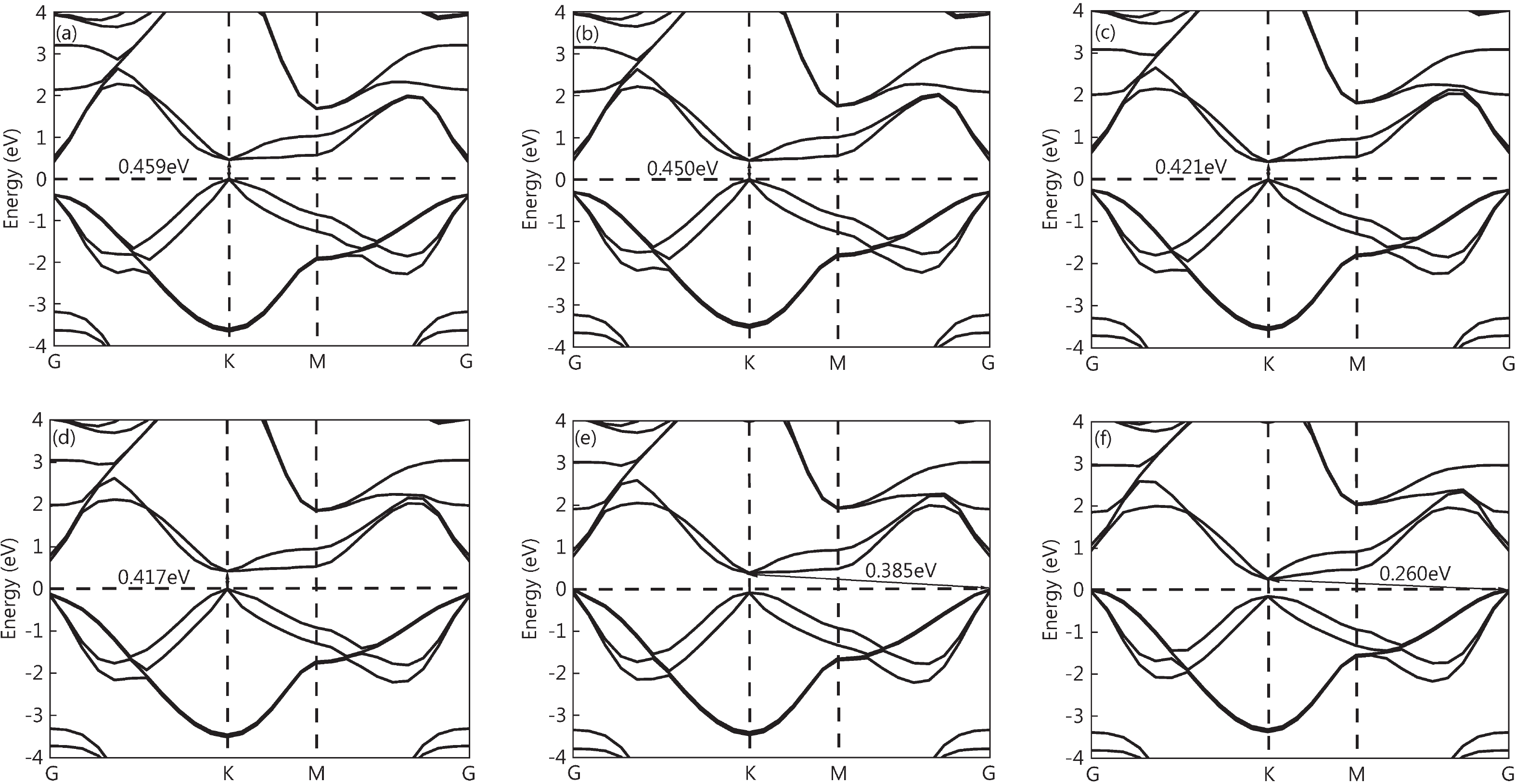
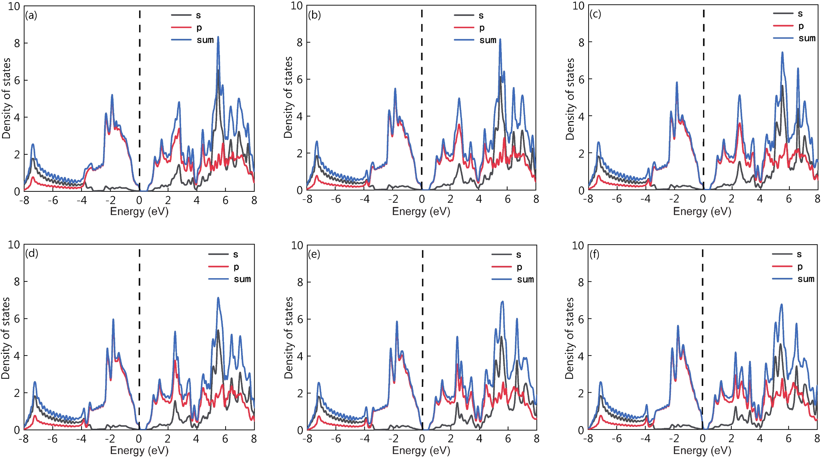
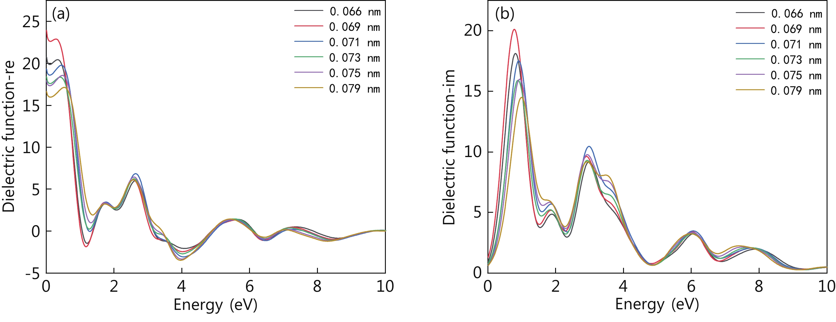
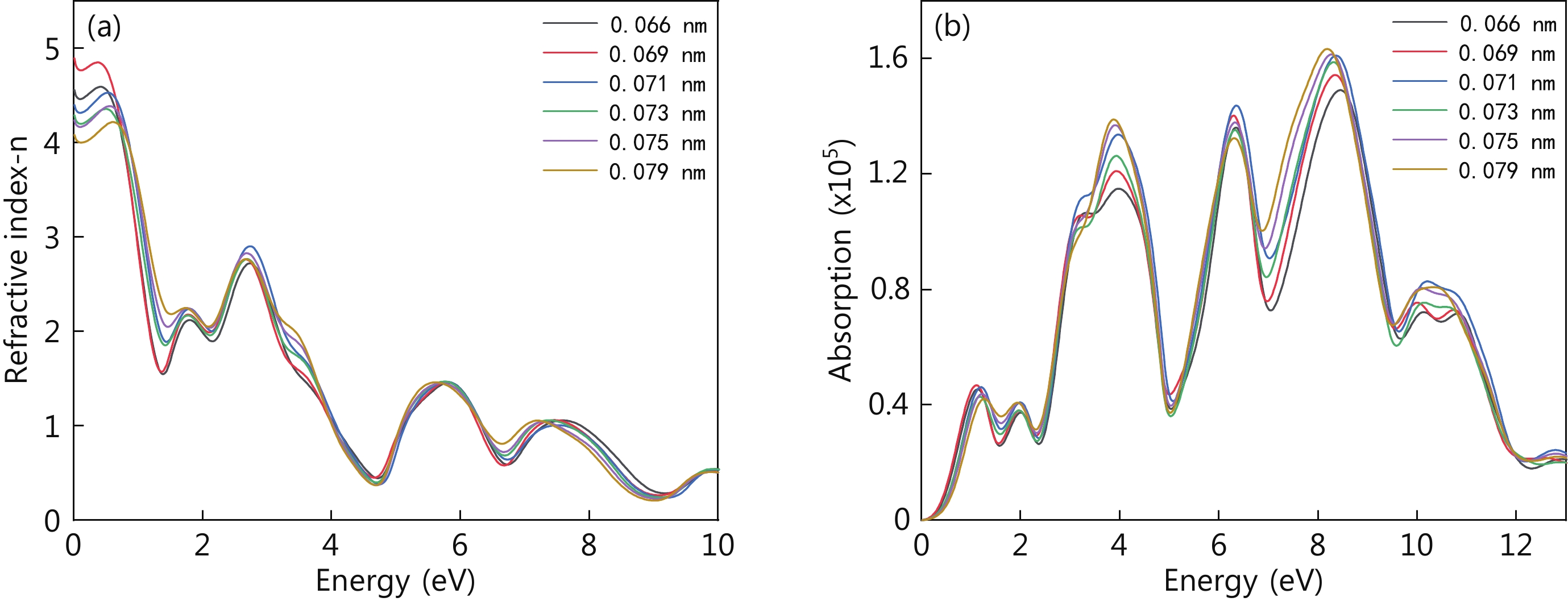
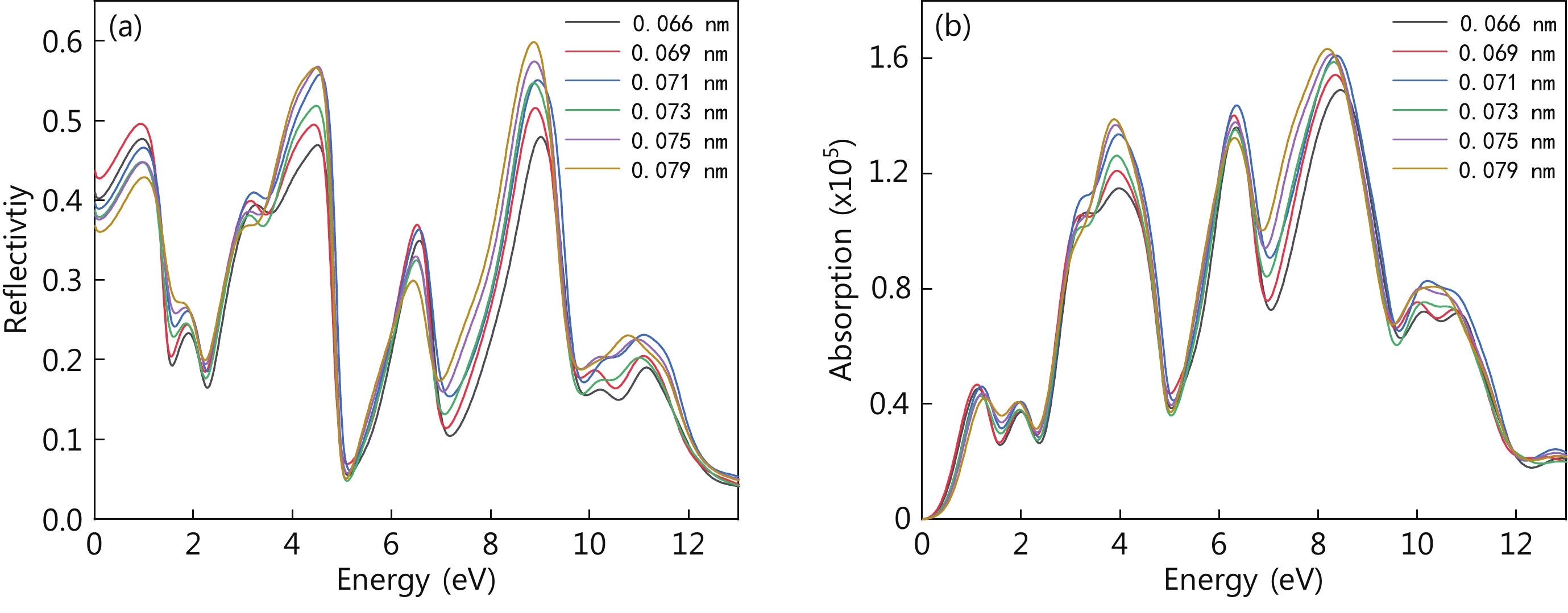
The electronic structure and optical properties of bilayer germanene under different warpages are studied by the first-principles method of density functional theory. The effects of warpages on the electronic structure and optical properties of bilayer germanene are analyzed. The results of the electronic structure study show that the bottom of the conduction band of bilayer germanene moves to the lower energy direction with the increase of warpages at the K point, and the top of the valence band stays constant at the K point, and so the band gap decreases with the increase of warpage. When the warpage is 0.075 nm, the top of the valence band of bilayer germanene changes from K point to G point, and the bilayer germanene becomes an indirect band gap semiconductor. This is an effective means to modulate the conversion of bilayer germanene between direct band gap semiconductor and indirect band gap semiconductor by adjusting the band structure of bilayer germanene effectively. The study of optical properties shows that the effect of warpage on the optical properties of bilayer germanene is mainly distributed in the ultraviolet and visible regions, and the warpage can effectively regulate the electronic structure and optical properties of bilayer germanene. When the warpage is 0.069 nm, the first peak of dielectric function and extinction coefficient is the largest, and the energy corresponding to the absorption band edge is the smallest. Therefore, the electron utilization rate is the best when the warpage is 0.069 nm. -
References
[1] Novoselov K S, Geim A K, Morozov S V, et al. Two-dimensional gas of massless Dirac fermions in graphene. Nature, 2005, 438, 197 doi: 10.1038/nature04233[2] Kara A, Enriquez H, Seitsonen A P, et al. A review on silicene — New candidate for electronics. Surf Sci Rep, 2012, 67, 1 doi: 10.1016/j.surfrep.2011.10.001[3] Cahangirov S, Topsakal M, Aktürk E, et al. Two- and one-dimensional honeycomb structures of silicon and germanium. Phys Rev Lett, 2009, 102, 236804 doi: 10.1103/PhysRevLett.102.236804[4] Behera H, Mukhopadhyay G. First-principles study of structural and electronic properties of germanene. AIP Conf Proc, 2011, 1349, 823 doi: 10.1063/1.3606111[5] Miro P, Audiffred M, Heine T. An atlas of two-dimensional materials. Chem Soc Rev, 2014, 43, 6537 doi: 10.1039/C4CS00102H[6] Kaloni T P. Tuning the structural, electronic, and magnetic properties of germanene by the adsorption of 3d transition metal atoms. J Phys Chem C, 2014, 118, 25200 doi: 10.1021/jp5058644[7] Hoshina Y, Iwasaki K, Yamada A, et al. First-principles analysis of indirect-to-direct band gap transition of Ge under tensile strain. Jpn J Appl Phys, 2009, 48, 04C125 doi: 10.1143/JJAP.48.04C125[8] Dhar N, Jana D. Effect of beryllium doping and vacancy in band structure, magnetic and optical properties of free standing germanene. Curr Appl Phys, 2017, 17, 1589 doi: 10.1016/j.cap.2017.08.022[9] Ni Z Y, Liu Q H, Tang K C, et al. Tunable bandgap in silicene and germanene. Nano Lett, 2012, 12, 113 doi: 10.1021/nl203065e[10] Hoat D M, Nguyen D K, Ponce-Pérez R, et al. Opening the germanene monolayer band gap using halogen atoms: An efficient approach studied by first-principles calculations. Appl Surf Sci, 2021, 551, 149318 doi: 10.1016/j.apsusc.2021.149318[11] Coello-Fiallos D, Tene T, Guayllas J L, et al. DFT comparison of structural and electronic properties of graphene and germanene: Monolayer and bilayer systems. Mater Today Proc, 2017, 4, 6835 doi: 10.1016/j.matpr.2017.07.011[12] Qin Z, Pan J, Lu S, et al. Direct evidence of Dirac signature in bilayer germanene islands on Cu (111). Adv Mater, 2017, 29, 1606046 doi: 10.1002/adma.201606046[13] McCann E, Fal'ko V I. Landau-level degeneracy and quantum Hall effect in a graphite bilayer. Phys Rev Lett, 2006, 96, 086805 doi: 10.1103/PhysRevLett.96.086805[14] McCann E. Asymmetry gap in the electronic band structure of bilayer graphene. Phys Rev B, 2006, 74, 161403 doi: 10.1103/PhysRevB.74.161403[15] Castro E V, Novoselov K S, Morozov S V, et al. Biased bilayer graphene: Semiconductor with a gap tunable by the electric field effect. Phys Rev Lett, 2007, 99, 216802 doi: 10.1103/PhysRevLett.99.216802[16] Nilsson J, Castro Neto A H. Impurities in a biased graphene bilayer. Phys Rev Lett, 2007, 98, 126801 doi: 10.1103/PhysRevLett.98.126801[17] Aoki M, Amawashi H. Dependence of band structures on stacking and field in layered graphene. Solid State Commun, 2007, 142, 123 doi: 10.1016/j.ssc.2007.02.013[18] Solís-Fernández P, Okada S, Sato T, et al. Gate-tunable Dirac point of molecular doped graphene. ACS Nano, 2016, 10, 2930 doi: 10.1021/acsnano.6b00064[19] Peres N M R. The electronic properties of graphene and its bilayer. Vacuum, 2009, 83, 1248 doi: 10.1016/j.vacuum.2009.03.018[20] Mañes J L, Guinea F, Vozmediano M A H. Existence and topological stability of Fermi points in multilayered graphene. Phys Rev B, 2007, 75, 155424 doi: 10.1103/PhysRevB.75.155424[21] Wang H, Zhou Q X, Ju W W, et al. Effect of vacancy defect and dopants on the sensitivity of germanene to H2CO. Phys E, 2022, 142, 115268 doi: 10.1016/j.physe.2022.115268[22] Hamid M A B, Chan K T, Raymond Ooi C H, et al. Structural stability and electronic properties of graphene/germanene heterobilayer. Results Phys, 2021, 28, 104545 doi: 10.1016/j.rinp.2021.104545[23] Raya S S, Ansari A S, Shong B. Adsorption of gas molecules on graphene, silicene, and germanene: A comparative first-principles study. Surf Interfaces, 2021, 24, 101054 doi: 10.1016/j.surfin.2021.101054[24] Zhang K, Sciacca D, Hanf M C, et al. Structure of germanene/Al(111): A two-layer surface alloy. J Phys Chem C, 2021, 125, 24702 doi: 10.1021/acs.jpcc.1c07585[25] Si X, She W H, Xu Q, et al. First-principles density functional theory study of modified germanene-based electrode materials. Materials, 2021, 15, 103 doi: 10.3390/ma15010103[26] Liu G, Luo W W, Wang X, et al. Tuning the electronic properties of germanene by molecular adsorption and under an external electric field. J Mater Chem C, 2018, 6, 5937 doi: 10.1039/C8TC01089G[27] Huong P T, Muoi D, Phuc H V, et al. Low-energy bands, optical properties, and spin/valley-Hall conductivity of silicene and germanene. J Mater Sci, 2020, 55, 14848 doi: 10.1007/s10853-020-05044-0[28] Chegel R, Behzad S. Tunable Electronic, Optical, and Thermal Properties of two-dimensional Germanene via an external electric field. Sci Rep, 2020, 10, 704 doi: 10.1038/s41598-020-57558-x[29] Kazemlou V, Phirouznia A. Influence of compression strains on photon absorption of silicene and germanene. Superlattices Microstruct, 2019, 128, 23 doi: 10.1016/j.spmi.2019.01.003[30] Segall M D, Lindan P J D, Probert M J, et al. First-principles simulation: Ideas, illustrations and the CASTEP code. J Phys: Condens Matter, 2002, 14, 2717 doi: 10.1088/0953-8984/14/11/301[31] Fischer T H, Jan A. General methods for geometry and wave function optimization. J Phys Chem, 1992, 96, 9768 doi: 10.1021/j100203a036 -
Proportional views


 DownLoad:
