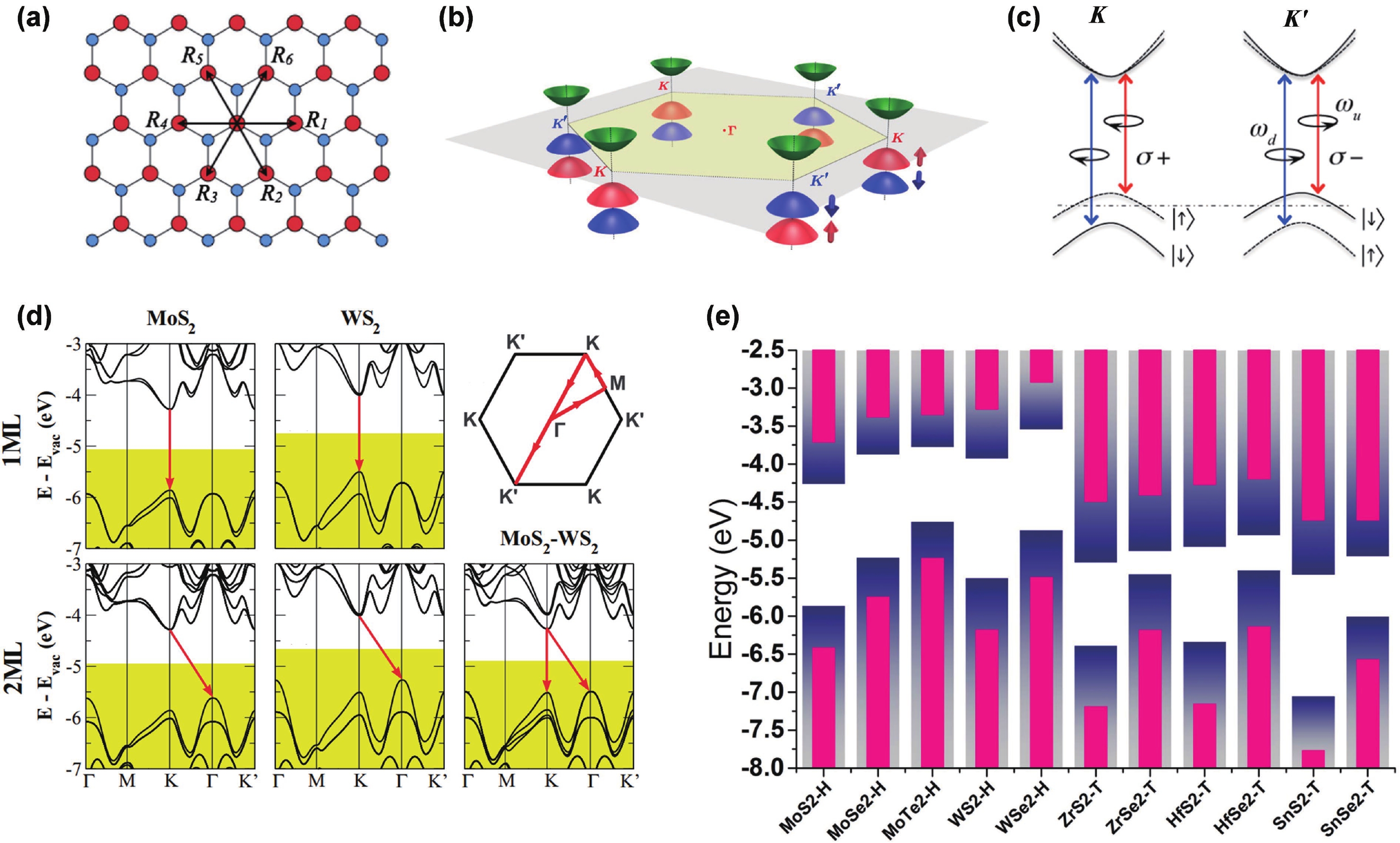
| [1] |
Rossetti R, Nakahara S, Brus L E. Quantum size effects in the redox potentials, resonance Raman spectra, and electronic spectra of CdS crystallites in aqueous solution. J Chem Phys, 1983, 79, 1086 doi: 10.1063/1.445834 |
| [2] |
Brus L E. Electron-electron and electron-hole interactions in small semiconductor crystallites: The size dependence of the lowest excited electronic state. J Chem Phys, 1984, 80, 4403 doi: 10.1063/1.447218 |
| [3] |
Chang C, Chen W, Chen Y, et al. Recent progress on two-dimensional materials. Acta Phys Chim Sinica, 2021, 37, 2108017 doi: 10.3866/PKU.WHXB202108017 |
| [4] |
Wu F C, Qu F Y, MacDonald A H. Exciton band structure of monolayer MoS 2. Phys Rev B, 2015, 91, 075310 doi: 10.1103/PhysRevB.91.075310 |
| [5] |
Ramasubramaniam A. Large excitonic effects in monolayers of molybdenum and tungsten dichalcogenides. Phys Rev B, 2012, 86, 115409 doi: 10.1103/PhysRevB.86.115409 |
| [6] |
Heo H, Sung J H, Cha S, et al. Interlayer orientation-dependent light absorption and emission in monolayer semiconductor stacks. Nat Commun, 2015, 6, 7372 doi: 10.1038/ncomms8372 |
| [7] |
Wang L, Meric I, Huang P Y, et al. One-dimensional electrical contact to a two-dimensional material. Science, 2013, 342, 614 doi: 10.1126/science.1244358 |
| [8] |
Kim K, Yankowitz M, Fallahazad B, et al. Van der waals heterostructures with high accuracy rotational alignment. Nano Lett, 2016, 16, 1989 doi: 10.1021/acs.nanolett.5b05263 |
| [9] |
Frisenda R, Navarro-Moratalla E, Gant P, et al. Recent progress in the assembly of nanodevices and van der Waals heterostructures by deterministic placement of 2D materials. Chem Soc Rev, 2018, 47, 53 doi: 10.1039/C7CS00556C |
| [10] |
Wang Y, Wang Z, Yao W, et al. Interlayer coupling in commensurate and incommensurate bilayer structures of transition-metal dichalcogenides. Phys Rev B, 2017, 95, 115429 doi: 10.1103/PhysRevB.95.115429 |
| [11] |
Regan E C, Wang D Q, Paik E Y, et al. Emerging exciton physics in transition metal dichalcogenide heterobilayers. Nat Rev Mater, 2022, 7, 778 doi: 10.1038/s41578-022-00440-1 |
| [12] |
Geim A K, Grigorieva I V. Van der waals heterostructures. Nature, 2013, 499, 419 doi: 10.1038/nature12385 |
| [13] |
Mak K F, Lee C G, Hone J, et al. Atomically thin MoS 2: A new direct-gap semiconductor. Phys Rev Lett, 2010, 105, 136805 doi: 10.1103/PhysRevLett.105.136805 |
| [14] |
Splendiani A, Sun L, Zhang Y B, et al. Emerging photoluminescence in monolayer MoS 2. Nano Lett, 2010, 10, 1271 doi: 10.1021/nl903868w |
| [15] |
Xiao D, Liu G B, Feng W X, et al. Coupled spin and valley physics in monolayers of MoS 2 and other group-VI dichalcogenides. Phys Rev Lett, 2012, 108, 196802 doi: 10.1103/PhysRevLett.108.196802 |
| [16] |
Xu X D, Yao W, Xiao D, et al. Spin and pseudospins in layered transition metal dichalcogenides. Nat Phys, 2014, 10, 343 doi: 10.1038/nphys2942 |
| [17] |
Li W J, Lu X, Wu J T, et al. Optical control of the valley Zeeman effect through many-exciton interactions. Nat Nanotechnol, 2021, 16, 148 doi: 10.1038/s41565-020-00804-0 |
| [18] |
Chernikov A, Berkelbach T C, Hill H M, et al. Exciton binding energy and nonhydrogenic rydberg series in monolayer WS 2. Phys Rev Lett, 2014, 113, 076802 doi: 10.1103/PhysRevLett.113.076802 |
| [19] |
Berkelbach T C, Hybertsen M S, Reichman D R, et al. Theory of neutral and charged excitons in monolayer transition metal dichalcogenides. Phys Rev B, 2013, 88, 045318 doi: 10.1103/PhysRevB.88.045318 |
| [20] |
Yao W, Xiao D, Niu Q. Valley-dependent optoelectronics from inversion symmetry breaking. Phys Rev B, 2008, 77, 235406 doi: 10.1103/PhysRevB.77.235406 |
| [21] |
Xiao D, Yao W, Niu Q. Valley-contrasting physics in graphene: Magnetic moment and topological transport. Phys Rev Lett, 2007, 99, 236809 doi: 10.1103/PhysRevLett.99.236809 |
| [22] |
Kośmider K, González J W, Fernández-Rossier J. Large spin splitting in the conduction band of transition metal dichalcogenide monolayers. Phys Rev B, 2013, 88, 245436 doi: 10.1103/PhysRevB.88.245436 |
| [23] |
Echeverry J P, Urbaszek B, Amand T, et al. Splitting between bright and dark excitons in transition metal dichalcogenide monolayers. Phys Rev B, 2016, 93, 121107 doi: 10.1103/PhysRevB.93.121107 |
| [24] |
Berghäuser G, Steinleitner P, Merkl P, et al. Mapping of the dark exciton landscape in transition metal dichalcogenides. Phys Rev B, 2018, 98, 020301 doi: 10.1103/PhysRevB.98.020301 |
| [25] |
Merkl P, Mooshammer F, Steinleitner P, et al. Ultrafast transition between exciton phases in van der Waals heterostructures. Nat Mater, 2019, 18, 691 doi: 10.1038/s41563-019-0337-0 |
| [26] |
Liu K H, Zhang L M, Cao T, et al. Evolution of interlayer coupling in twisted molybdenum disulfide bilayers. Nat Commun, 2014, 5, 4966 doi: 10.1038/ncomms5966 |
| [27] |
van der Zande A M, Kunstmann J, Chernikov A, et al. Tailoring the electronic structure in bilayer molybdenum disulfide via interlayer twist. Nano Lett, 2014, 14, 3869 doi: 10.1021/nl501077m |
| [28] |
Meckbach L, Stroucken T, Koch S W. Influence of the effective layer thickness on the ground-state and excitonic properties of transition-metal dichalcogenide systems. Phys Rev B, 2018, 97, 035425 doi: 10.1103/PhysRevB.97.035425 |
| [29] |
Horng J, Stroucken T, Zhang L, et al. Observation of interlayer excitons in MoSe 2 single crystals. Phys Rev B, 2018, 97, 241404 doi: 10.1103/PhysRevB.97.241404 |
| [30] |
Arora A, Drüppel M, Schmidt R, et al. Interlayer excitons in a bulk van der Waals semiconductor. Nat Commun, 2017, 8, 639 doi: 10.1038/s41467-017-00691-5 |
| [31] |
Kośmider K, Fernández-Rossier J. Electronic properties of the MoS 2-WS 2 heterojunction. Phys Rev B, 2013, 87, 075451 doi: 10.1103/PhysRevB.87.075451 |
| [32] |
Zhang C X, Gong C, Nie Y F, et al. Systematic study of electronic structure and band alignment of monolayer transition metal dichalcogenides in Van der Waals heterostructures. 2D Mater, 2016, 4, 015026 doi: 10.1088/2053-1583/4/1/015026 |
| [33] |
Chen Y F, Xi J Y, Dumcenco D O, et al. Tunable band gap photoluminescence from atomically thin transition-metal dichalcogenide alloys. ACS Nano, 2013, 7, 4610 doi: 10.1021/nn401420h |
| [34] |
Gong C, Zhang H J, Wang W H, et al. Band alignment of two-dimensional transition metal dichalcogenides: Application in tunnel field effect transistors. Appl Phys Lett, 2013, 103, 053513 doi: 10.1063/1.4817409 |
| [35] |
Hong X P, Kim J, Shi S F, et al. Ultrafast charge transfer in atomically thin MoS 2/WS 2 heterostructures. Nat Nanotechnol, 2014, 9, 682 doi: 10.1038/nnano.2014.167 |
| [36] |
Xu W G, Liu W W, Schmidt J F, et al. Correlated fluorescence blinking in two-dimensional semiconductor heterostructures. Nature, 2017, 541, 62 doi: 10.1038/nature20601 |
| [37] |
Fang H, Battaglia C, Carraro C, et al. Strong interlayer coupling in van der Waals heterostructures built from single-layer chalcogenides. Proc Natl Acad Sci USA, 2014, 111, 6198 doi: 10.1073/pnas.1405435111 |
| [38] |
Kadantsev E S, et al. Electronic structure of a single MoS 2 monolayer. Solid State Commun, 2012, 152, 909 doi: 10.1016/j.ssc.2012.02.005 |
| [39] |
Li H, Li H L, Wang X Z, et al. Spontaneous polarity flipping in a 2D heterobilayer induced by fluctuating interfacial carrier flows. Nano Lett, 2021, 21, 6773 doi: 10.1021/acs.nanolett.1c01356 |
| [40] |
Xia J, Yan J X, Wang Z H, et al. Strong coupling and pressure engineering in WSe 2–MoSe 2 heterobilayers. Nat Phys, 2021, 17, 92 doi: 10.1038/s41567-020-1005-7 |
| [41] |
Komsa H P, Krasheninnikov A V. Electronic structures and optical properties of realistic transition metal dichalcogenide heterostructures from first principles. Phys Rev B, 2013, 88, 085318 doi: 10.1103/PhysRevB.88.085318 |
| [42] |
Zhu H M, Wang J, Gong Z Z, et al. Interfacial charge transfer circumventing momentum mismatch at two-dimensional van der waals heterojunctions. Nano Lett, 2017, 17, 3591 doi: 10.1021/acs.nanolett.7b00748 |
| [43] |
Zeng Y, Dai W, Ma R D, et al. Distinguishing ultrafast energy transfer in atomically thin MoS 2/WS 2 heterostructures. Small, 2022, 18, e2204317 doi: 10.1002/smll.202204317 |
| [44] |
Hu Z, Liu X, Hernández-Martínez P L et al. Interfacial charge and energy transfer in van der Waals heterojunctions. InfoMat, 2022, 4(3), e12290 doi: 10.1002/inf2.12290 |
| [45] |
Kozawa D, Carvalho A, Verzhbitskiy I, et al. Evidence for fast interlayer energy transfer in MoSe 2/WS 2 heterostructures. Nano Lett, 2016, 16, 4087 doi: 10.1021/acs.nanolett.6b00801 |
| [46] |
Wu L L, Chen Y Z, Zhou H Z, et al. Ultrafast energy transfer of both bright and dark excitons in 2D van der waals heterostructures beyond dipolar coupling. ACS Nano, 2019, 13, 2341 doi: 10.1021/acsnano.8b09059 |
| [47] |
Zhou H Z, Zhao Y D, Tao W J, et al. Controlling exciton and valley dynamics in two-dimensional heterostructures with atomically precise interlayer proximity. ACS Nano, 2020, 14, 4618 doi: 10.1021/acsnano.0c00218 |
| [48] |
Hu Z H, Hernández-Martínez P L, Liu X, et al. Trion-mediated Förster resonance energy transfer and optical gating effect in WS 2/hBN/MoSe 2 heterojunction. ACS Nano, 2020, 14, 13470 doi: 10.1021/acsnano.0c05447 |
| [49] |
Lyo S K. Energy transfer from an electron-hole plasma layer to a quantum well in semiconductor structures. Phys Rev B, 2010, 81, 115303 doi: 10.1103/PhysRevB.81.115303 |
| [50] |
|
| [51] |
Marcus R A, et al. Electron transfers in chemistry and biology. Biochim Biophys Acta Rev Bioenerg, 1985, 811, 265 doi: 10.1016/0304-4173(85)90014-X |
| [52] |
Ji Z H, Hong H, Zhang J, et al. Robust stacking-independent ultrafast charge transfer in MoS 2/WS 2 bilayers. ACS Nano, 2017, 11, 12020 doi: 10.1021/acsnano.7b04541 |
| [53] |
Zhu X Y, Monahan N R, Gong Z Z, et al. Charge transfer excitons at van der waals interfaces. J Am Chem Soc, 2015, 137, 8313 doi: 10.1021/jacs.5b03141 |
| [54] |
Godiksen R H, Wang S J, Raziman T V, et al. Correlated exciton fluctuations in a two-dimensional semiconductor on a metal. Nano Lett, 2020, 20, 4829 doi: 10.1021/acs.nanolett.0c00756 |
| [55] |
Merkl P, Mooshammer F, Brem S, et al. Twist-tailoring Coulomb correlations in van der Waals homobilayers. Nat Commun, 2020, 11, 2167 doi: 10.1038/s41467-020-16069-z |
| [56] |
Wu K, Zhong H X, Guo Q B, et al. Identification of twist-angle-dependent excitons in WS 2/WSe 2 heterobilayers. Natl Sci Rev, 2021, 9, nwab135 doi: 10.1093/nsr/nwab135 |
| [57] |
Zheng Q J, Saidi W A, Xie Y, et al. Phonon-assisted ultrafast charge transfer at van der waals heterostructure interface. Nano Lett, 2017, 17, 6435 doi: 10.1021/acs.nanolett.7b03429 |
| [58] |
Wang K, Huang B, Tian M K, et al. Interlayer coupling in twisted WSe 2/WS 2 bilayer heterostructures revealed by optical spectroscopy. ACS Nano, 2016, 10, 6612 doi: 10.1021/acsnano.6b01486 |
| [59] |
Rivera P, Schaibley J R, Jones A M, et al. Observation of long-lived interlayer excitons in monolayer MoSe 2–WSe 2 heterostructures. Nat Commun, 2015, 6, 6242 doi: 10.1038/ncomms7242 |
| [60] |
Raja A, Chaves A, Yu J, et al. Coulomb engineering of the bandgap and excitons in two-dimensional materials. Nat Commun, 2017, 8, 15251 doi: 10.1038/ncomms15251 |
| [61] |
Waldecker L, Raja A, Rösner M, et al. Rigid band shifts in two-dimensional semiconductors through external dielectric screening. Phys Rev Lett, 2019, 123, 206403 doi: 10.1103/PhysRevLett.123.206403 |
| [62] |
Amani M, Lien D H, Kiriya D, et al. Near-unity photoluminescence quantum yield in MoS 2. Science, 2015, 350, 1065 doi: 10.1126/science.aad2114 |
| [63] |
Lien D H, Uddin S Z, Yeh M, et al. Electrical suppression of all nonradiative recombination pathways in monolayer semiconductors. Science, 2019, 364, 468 doi: 10.1126/science.aaw8053 |
| [64] |
Kim H, Uddin S Z, Higashitarumizu N, et al. Inhibited nonradiative decay at all exciton densities in monolayer semiconductors. Science, 2021, 373, 448 doi: 10.1126/science.abi9193 |
| [65] |
Zhu Z Y, Cheng Y C, Schwingenschlögl U. Giant spin-orbit-induced spin splitting in two-dimensional transition-metal dichalcogenide semiconductors. Phys Rev B, 2011, 84, 153402 doi: 10.1103/PhysRevB.84.153402 |
| [66] |
Liu G B, Xiao D, Yao Y G, et al. Electronic structures and theoretical modelling of two-dimensional group-VIB transition metal dichalcogenides. Chem Soc Rev, 2015, 44, 2643 doi: 10.1039/C4CS00301B |
| [67] |
Zhao W J, Ghorannevis Z, Chu L Q, et al. Evolution of electronic structure in atomically thin sheets of WS 2 and WSe 2. ACS Nano, 2013, 7, 791 doi: 10.1021/nn305275h |
| [68] |
Zeng H L, Liu G B, Dai J F, et al. Optical signature of symmetry variations and spin-valley coupling in atomically thin tungsten dichalcogenides. Sci Rep, 2013, 3, 1608 doi: 10.1038/srep01608 |
| [69] |
Wilson J A, Yoffe A D. The transition metal dichalcogenides discussion and interpretation of the observed optical, electrical and structural properties. Adv Phys, 1969, 18, 193 doi: 10.1080/00018736900101307 |
| [70] |
Arora A, Koperski M, Nogajewski K, et al. Excitonic resonances in thin films of WSe 2: From monolayer to bulk material. Nanoscale, 2015, 7, 10421 doi: 10.1039/C5NR01536G |
| [71] |
Kozawa D, Kumar R, Carvalho A, et al. Photocarrier relaxation pathway in two-dimensional semiconducting transition metal dichalcogenides. Nat Commun, 2014, 5, 4543 doi: 10.1038/ncomms5543 |
| [72] |
Kim M S, Seo C, Kim H, et al. Simultaneous hosting of positive and negative trions and the enhanced direct band emission in MoSe 2/MoS 2 heterostacked multilayers. ACS Nano, 2016, 10, 6211 doi: 10.1021/acsnano.6b02213 |
| [73] |
Lampert M A. Mobile and immobile effective-mass-particle complexes in nonmetallic solids. Phys Rev Lett, 1958, 1, 450 doi: 10.1103/PhysRevLett.1.450 |
| [74] |
Kheng K, Cox R T, My D A, et al. Observation of negatively charged excitons X- in semiconductor quantum wells. Phys Rev Lett, 1993, 71, 1752 doi: 10.1103/PhysRevLett.71.1752 |
| [75] |
Finkelstein G, Shtrikman H. Optical spectroscopy of a two-dimensional electron gas near the metal-insulator transition. Phys Rev Lett, 1995, 74, 976 doi: 10.1103/PhysRevLett.74.976 |
| [76] |
Ross J S, Wu S F, Yu H Y, et al. Electrical control of neutral and charged excitons in a monolayer semiconductor. Nat Commun, 2013, 4, 1474 doi: 10.1038/ncomms2498 |
| [77] |
Mak K F, He K L, Lee C G, et al. Tightly bound trions in monolayer MoS 2. Nat Mater, 2013, 12, 207 doi: 10.1038/nmat3505 |
| [78] |
Nagourney W, Sandberg J, Dehmelt H. Shelved optical electron amplifier: Observation of quantum jumps. Phys Rev Lett, 1986, 56, 2797 doi: 10.1103/PhysRevLett.56.2797 |
| [79] |
Basché T, Kummer S, Bräuchle C. Direct spectroscopic observation of quantum jumps of a single molecule. Nature, 1995, 373, 132 doi: 10.1038/373132a0 |
| [80] |
Dickson R M, Cubitt A B, Tsien R Y, et al. On/off blinking and switching behaviour of single molecules of green fluorescent protein. Nature, 1997, 388, 355 doi: 10.1038/41048 |
| [81] |
Galland C, Ghosh Y, Steinbrück A, et al. Two types of luminescence blinking revealed by spectroelectrochemistry of single quantum dots. Nature, 2011, 479, 203 doi: 10.1038/nature10569 |
| [82] |
Wu F C, Lovorn T, MacDonald A H. Topological exciton bands in moiré heterojunctions. Phys Rev Lett, 2017, 118, 147401 doi: 10.1103/PhysRevLett.118.147401 |
| [83] |
Zhang N, Surrente A, Baranowski M, et al. Moiré intralayer excitons in a MoSe 2/MoS 2 heterostructure. Nano Lett, 2018, 18, 7651 doi: 10.1021/acs.nanolett.8b03266 |
| [84] |
Tang Y H, Gu J, Liu S, et al. Tuning layer-hybridized moiré excitons by the quantum-confined Stark effect. Nat Nanotechnol, 2021, 16, 52 doi: 10.1038/s41565-020-00783-2 |
| [85] |
Jin C H, Regan E C, Yan A M, et al. Observation of moiré excitons in WSe 2/WS 2 heterostructure superlattices. Nature, 2019, 567, 76 doi: 10.1038/s41586-019-0976-y |
| [86] |
Tang Y H, Li L Z, Li T X, et al. Simulation of Hubbard model physics in WSe 2/WS 2 moiré superlattices. Nature, 2020, 579, 353 doi: 10.1038/s41586-020-2085-3 |
| [87] |
Wu B, Zheng H H, Li S F, et al. Observation of moiré excitons in the twisted WS 2/WS 2 homostructure. Nanoscale, 2022, 14, 12447 doi: 10.1039/D2NR02450K |
| [88] |
Andersen T I, Scuri G, Sushko A, et al. Excitons in a reconstructed moiré potential in twisted WSe 2/WSe 2 homobilayers. Nat Mater, 2021, 20, 480 doi: 10.1038/s41563-020-00873-5 |
| [89] |
Wu B, Zheng H H, Li S F, et al. Evidence for moiré intralayer excitons in twisted WSe 2/WSe 2 homobilayer superlattices. Light Sci Appl, 2022, 11, 166 doi: 10.1038/s41377-022-00854-0 |
| [90] |
Liu Y D, Elbanna A, Gao W B, et al. Interlayer excitons in transition metal dichalcogenide semiconductors for 2D optoelectronics. Adv Mater, 2022, 34, e2107138 doi: 10.1002/adma.202107138 |
| [91] |
Liu Y P, Zeng C, Yu J, et al. Moiré superlattices and related moiré excitons in twisted van der Waals heterostructures. Chem Soc Rev, 2021, 50, 6401 doi: 10.1039/D0CS01002B |
| [92] |
Jiang C Y, Xu W G, Rasmita A, et al. Microsecond dark-exciton valley polarization memory in two-dimensional heterostructures. Nat Commun, 2018, 9, 753 doi: 10.1038/s41467-018-03174-3 |
| [93] |
Dufferwiel S, Schwarz S, Withers F, et al. Exciton–polaritons in van der Waals heterostructures embedded in tunable microcavities. Nat Commun, 2015, 6, 8579 doi: 10.1038/ncomms9579 |
| [94] |
Wang Z F, Rhodes D A, Watanabe K, et al. Evidence of high-temperature exciton condensation in two-dimensional atomic double layers. Nature, 2019, 574, 76 doi: 10.1038/s41586-019-1591-7 |
| [95] |
Ji J, Choi J H. Recent progress in 2D hybrid heterostructures from transition metal dichalcogenides and organic layers: Properties and applications in energy and optoelectronics fields. Nanoscale, 2022, 14, 10648 doi: 10.1039/D2NR01358D |
| [96] |
Sulas-Kern D B, Miller E M, Blackburn J L. Photoinduced charge transfer in transition metal dichalcogenide heterojunctions - towards next generation energy technologies. Energy Environ Sci, 2020, 13, 2684 doi: 10.1039/D0EE01370F |
| [97] |
Nayak P K, Horbatenko Y, Ahn S, et al. Probing evolution of twist-angle-dependent interlayer excitons in MoSe 2/WSe 2 van der waals heterostructures. ACS Nano, 2017, 11, 4041 doi: 10.1021/acsnano.7b00640 |
| [98] |
Rivera P, Seyler K L, Yu H Y, et al. Valley-polarized exciton dynamics in a 2D semiconductor heterostructure. Science, 2016, 351, 688 doi: 10.1126/science.aac7820 |
| [99] |
Marcellina E, Liu X, Hu Z H, et al. Evidence for moiré trions in twisted MoSe 2 homobilayers. Nano Lett, 2021, 21, 4461 doi: 10.1021/acs.nanolett.1c01207 |
| [100] |
Kunstmann J, Mooshammer F, Nagler P, et al. Momentum-space indirect interlayer excitons in transition-metal dichalcogenide van der Waals heterostructures. Nat Phys, 2018, 14, 801 doi: 10.1038/s41567-018-0123-y |
| [101] |
Yan W, Meng L, Meng Z S, et al. Probing angle-dependent interlayer coupling in twisted bilayer WS 2. J Phys Chem C, 2019, 123, 30684 doi: 10.1021/acs.jpcc.9b08602 |
| [102] |
Hanbicki A T, Chuang H J, Rosenberger M R, et al. Double indirect interlayer exciton in a MoSe 2/WSe 2 van der waals heterostructure. ACS Nano, 2018, 12, 4719 doi: 10.1021/acsnano.8b01369 |
| [103] |
Yu H Y, Liu G B, Yao W. Brightened spin-triplet interlayer excitons and optical selection rules in van der Waals heterobilayers. 2D Mater, 2018, 5, 035021 doi: 10.1088/2053-1583/aac065 |
| [104] |
Tan Q H, Rasmita A, Li S, et al. Layer-engineered interlayer excitons. Sci Adv, 2021, 7, eabh0863 doi: 10.1126/sciadv.abh0863 |
| [105] |
Liu E F, Barré E, van Baren J, et al. Signatures of moiré trions in WSe 2/MoSe 2 heterobilayers. Nature, 2021, 594, 46 doi: 10.1038/s41586-021-03541-z |
| [106] |
Tran K, Moody G, Wu F C, et al. Evidence for moiré excitons in van der waals heterostructures. Nature, 2019, 567, 71 doi: 10.1038/s41586-019-0975-z |
| [107] |
Yu H Y, Wang Y, Tong Q J, et al. Anomalous light cones and valley optical selection rules of interlayer excitons in twisted heterobilayers. Phys Rev Lett, 2015, 115, 187002 doi: 10.1103/PhysRevLett.115.187002 |
| [108] |
Wu F C, Lovorn T, MacDonald A H. Theory of optical absorption by interlayer excitons in transition metal dichalcogenide heterobilayers. Phys Rev B, 2018, 97, 035306 doi: 10.1103/PhysRevB.97.035306 |
| [109] |
Yu H Y, Liu G B, Tang J J, et al. Moiré excitons: From programmable quantum emitter arrays to spin-orbit-coupled artificial lattices. Sci Adv, 2017, 3, e1701696 doi: 10.1126/sciadv.1701696 |
| [110] |
Brotons-Gisbert M, Baek H, Molina-Sánchez A, et al. Spin-layer locking of interlayer excitons trapped in moiré potentials. Nat Mater, 2020, 19, 630 doi: 10.1038/s41563-020-0687-7 |
| [111] |
Jiang Y, Chen S L, Zheng W H, et al. Interlayer exciton formation, relaxation, and transport in TMD van der Waals heterostructures. Light Sci Appl, 2021, 10, 72 doi: 10.1038/s41377-021-00500-1 |
| [112] |
Shi B B, Qi P F, Jiang M L, et al. Exotic physical properties of 2D materials modulated by moiré superlattices. Mater Adv, 2021, 2, 5542 doi: 10.1039/D1MA00263E |
| [113] |
Zhang H Z, Wu W J, Zhou L, et al. Steering on degrees of freedom of 2D van der waals heterostructures. Small Sci, 2022, 2, 2100033 doi: 10.1002/smsc.202100033 |
| [114] |
He F, Zhou Y J, Ye Z F, et al. Moiré patterns in 2D materials: A review. ACS Nano, 2021, 15, 5944 doi: 10.1021/acsnano.0c10435 |
| [115] |
Baek H, Brotons-Gisbert M, Campbell A, et al. Optical read-out of Coulomb staircases in a moiré superlattice via trapped interlayer trions. Nat Nanotechnol, 2021, 16, 1237 doi: 10.1038/s41565-021-00970-9 |
| [116] |
Bai Y S, Zhou L, Wang J, et al. Excitons in strain-induced one-dimensional moiré potentials at transition metal dichalcogenide heterojunctions. Nat Mater, 2020, 19, 1068 doi: 10.1038/s41563-020-0730-8 |
| [117] |
Wang X, Zhu J Y, Seyler K L, et al. Moiré trions in MoSe 2/WSe 2 heterobilayers. Nat Nanotechnol, 2021, 16, 1208 doi: 10.1038/s41565-021-00969-2 |
| [118] |
Shinokita K, Miyauchi Y, Watanabe K, et al. Resonant coupling of a moiré exciton to a phonon in a WSe 2/MoSe 2 heterobilayer. Nano Lett, 2021, 21, 5938 doi: 10.1021/acs.nanolett.1c00733 |
| [119] |
Baek H, Brotons-Gisbert M, Koong Z X, et al. Highly energy-tunable quantum light from moiré-trapped excitons. Sci Adv, 2020, 6, eaba8526 doi: 10.1126/sciadv.aba8526 |
| [120] |
He Y M, Clark G, Schaibley J R, et al. Single quantum emitters in monolayer semiconductors. Nat Nanotechnol, 2015, 10, 497 doi: 10.1038/nnano.2015.75 |
| [121] |
Srivastava A, Sidler M, Allain A V, et al. Optically active quantum dots in monolayer WSe 2. Nat Nanotechnol, 2015, 10, 491 doi: 10.1038/nnano.2015.60 |
| [122] |
Koperski M, Nogajewski K, Arora A, et al. Single photon emitters in exfoliated WSe 2 structures. Nat Nanotechnol, 2015, 10, 503 doi: 10.1038/nnano.2015.67 |
| [123] |
Chakraborty C, Kinnischtzke L, Goodfellow K M, et al. Voltage-controlled quantum light from an atomically thin semiconductor. Nat Nanotechnol, 2015, 10, 507 doi: 10.1038/nnano.2015.79 |
| [124] |
Lu X, Chen X T, Dubey S, et al. Optical initialization of a single spin-valley in charged WSe 2 quantum dots. Nat Nanotechnol, 2019, 14, 426 doi: 10.1038/s41565-019-0394-1 |
| [125] |
Chen X T, Lu X, Dubey S, et al. Entanglement of single-photons and chiral phonons in atomically thin WSe 2. Nat Phys, 2019, 15, 221 doi: 10.1038/s41567-018-0366-7 |
| [126] |
Seyler K L, Rivera P, Yu H Y, et al. Signatures of moiré-trapped valley excitons in MoSe 2/WSe 2 heterobilayers. Nature, 2019, 567, 66 doi: 10.1038/s41586-019-0957-1 |
| [127] |
Li W J, Lu X, Dubey S, et al. Dipolar interactions between localized interlayer excitons in van der Waals heterostructures. Nat Mater, 2020, 19, 624 doi: 10.1038/s41563-020-0661-4 |
| [128] |
Fogler M M, Butov L V, Novoselov K S. High-temperature superfluidity with indirect excitons in van der Waals heterostructures. Nat Commun, 2014, 5, 4555 doi: 10.1038/ncomms5555 |
| [129] |
Snoke D. Spontaneous Bose coherence of excitons and polaritons. Science, 2002, 298, 1368 doi: 10.1126/science.1078082 |
| [130] |
Unuchek D, Ciarrocchi A, Avsar A, et al. Room-temperature electrical control of exciton flux in a van der Waals heterostructure. Nature, 2018, 560, 340 doi: 10.1038/s41586-018-0357-y |
| [131] |
Unuchek D, Ciarrocchi A, Avsar A, et al. Valley-polarized exciton currents in a van der Waals heterostructure. Nat Nanotechnol, 2019, 14, 1104 doi: 10.1038/s41565-019-0559-y |
| [132] |
Ciarrocchi A, Unuchek D, Avsar A, et al. Polarization switching and electrical control of interlayer excitons in two-dimensional van der Waals heterostructures. Nat Photonics, 2019, 13, 131 doi: 10.1038/s41566-018-0325-y |
| [133] |
Liu Y D, Fang H L, Rasmita A, et al. Room temperature nanocavity laser with interlayer excitons in 2D heterostructures. Sci Adv, 2019, 5, eaav4506 doi: 10.1126/sciadv.aav4506 |
| [134] |
Paik E Y, Zhang L, Burg G W, et al. Interlayer exciton laser of extended spatial coherence in atomically thin heterostructures. Nature, 2019, 576, 80 doi: 10.1038/s41586-019-1779-x |
| [135] |
Lukman S, Ding L, Xu L, et al. High oscillator strength interlayer excitons in two-dimensional heterostructures for mid-infrared photodetection. Nat Nanotechnol, 2020, 15, 675 doi: 10.1038/s41565-020-0717-2 |
| [136] |
Park S, Kim D, Seo M K. Plasmonic photonic crystal mirror for long-lived interlayer exciton generation. ACS Photonics, 2021, 8, 3619 doi: 10.1021/acsphotonics.1c01243 |
| [137] |
Tran T N, Kim S, White S J U, et al. Enhanced emission from interlayer excitons coupled to plasmonic gap cavities. Small, 2021, 17, e2103994 doi: 10.1002/smll.202103994 |
| [138] |
Yuan L, Zheng B Y, Kunstmann J, et al. Twist-angle-dependent interlayer exciton diffusion in WS 2–WSe 2 heterobilayers. Nat Mater, 2020, 19, 617 doi: 10.1038/s41563-020-0670-3 |
| [139] |
Alexeev E M, Ruiz-Tijerina D A, Danovich M, et al. Resonantly hybridized excitons in moiré superlattices in van der waals heterostructures. Nature, 2019, 567, 81 doi: 10.1038/s41586-019-0986-9 |
| [140] |
Zhang L, Gogna R, Burg G W, et al. Highly valley-polarized singlet and triplet interlayer excitons in van der waals heterostructure. Phys Rev B, 2019, 100, 041402 doi: 10.1103/PhysRevB.100.041402 |
| [141] |
Enaldiev V V, Ferreira F, McHugh J G, et al. Self-organized quantum dots in marginally twisted MoSe 2/WSe 2 and MoS 2/WS 2 bilayers. npj 2D Mater Appl, 2022, 6, 74 doi: 10.1038/s41699-022-00346-0 |


 DownLoad:


 Hua Li:got her BS degree in 2015 and MS degree in 2018 at Lanzhou University. She then joined Weigao Xu’s group and got her PhD degree in 2021 at Nanjing University. Now she is an associate research fellow at Nanjing University. Her research interest focuses on the optical spectroscopy and microscopic imaging at the interfaces
 Jinyang Ling:received his BS degree in Chemistry from Nanjing University in 2021 and is currently pursuing his MS in Physical Chemistry under the supervision of Prof. Weigao Xu at the School of Chemistry and Chemical Engineering in Nanjing University. His research focuses on the excitonic dynamics of 2D layered materials in the in-plane direction, and corresponding excitonic optoelectronic devices
 Jiamin Lin:received her BS degree in Materials Science and Engineering from Nanjing University of Science and Technology in 2020 and she is currently pursuing her PhD at institute of Chemistry and Chemical Engineering, Nanjing University, under the supervision of Prof. Weigao Xu. Her research interests include low-dimensional materials and their optothermal transport behavior
 Xin Lu:earned her bachelor’s degree from Wuhan University in 2012, and her PhD from Nanyang Technological University in 2017. Subsequently, Lu joined Prof. Ajit Srivastava’s group at Emory University as a postdoctoral researcher. Since January 2021, Lu has started as an Assistant Professor in the Department of Physics and Engineering Physics at Tulane University. Her research focuses on optical spectroscopy of low-dimensional materials
 Weigao Xu:got his BS degree in 2008 at Lanzhou University and PhD degree in 2013 at Peking University. Then he joined Qihua Xiong’s group as a postdoc at Nanyang Technological University in Singapore. In March 2018, he joined Nanjing University as a full professor. His research interest focuses on the bottom-up assembly of meso-scale materials from nanomaterial units, the discovery of their optical, electrical, mechanical, and chemical properties, and the development of their functionalities


