


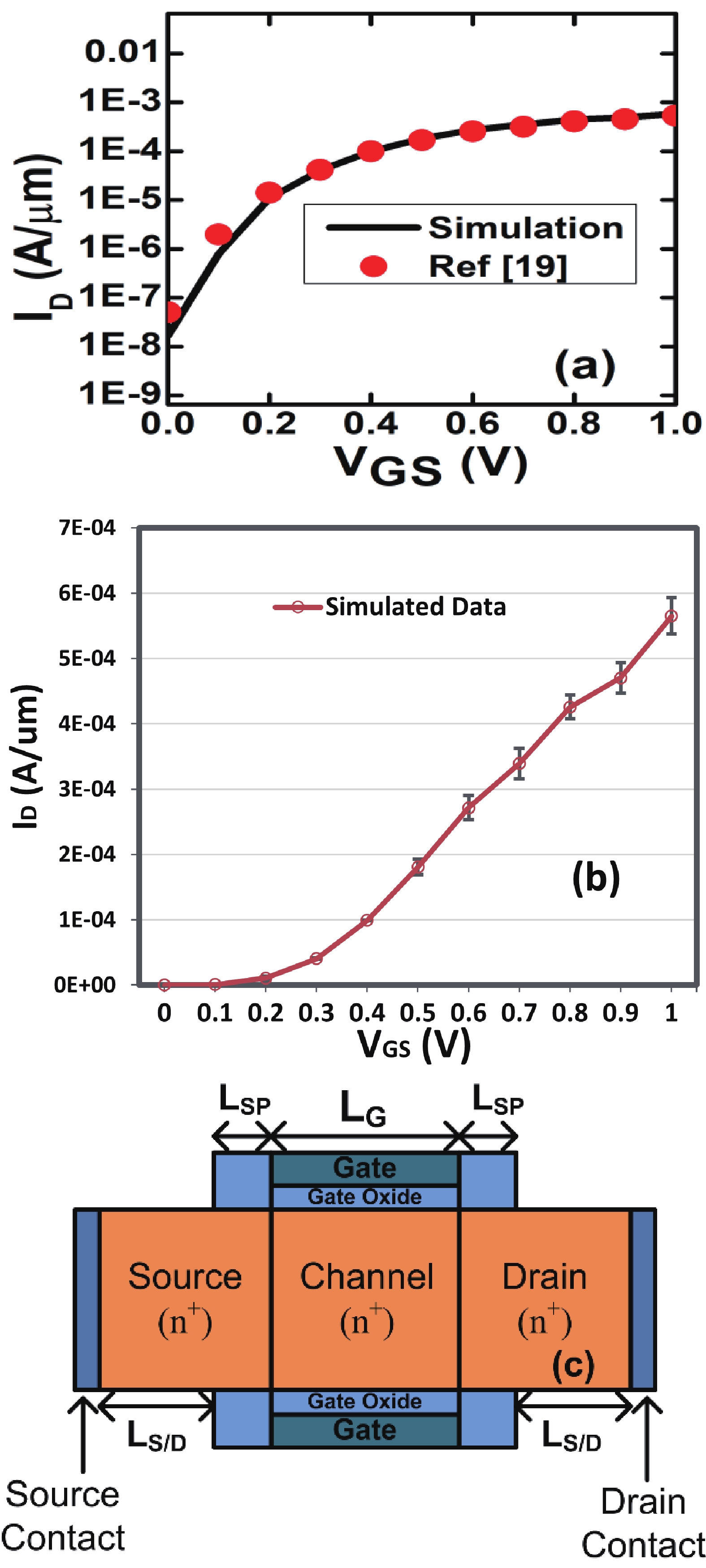
Fig. 1.
(Color online) (a) Calibration of the tool against the experimental data presented in Ref. [19]. (b) Simulated I−V curve with error bars. (c) Cross-sectional representation of the junctionless FinFET device.
ARTICLES
Devenderpal Singh, Shalini Chaudhary, Basudha Dewan and Menka Yadav
Corresponding author: Devenderpal Singh, 2020rec9502@mnit.ac.in
Abstract: This manuscript explores the behavior of a junctionless tri-gate FinFET at the nano-scale region using SiGe material for the channel. For the analysis, three different channel structures are used: (a) tri-layer stack channel (TLSC) (Si–SiGe–Si), (b) double layer stack channel (DLSC) (SiGe–Si), (c) single layer channel (SLC) (Si). The I−V characteristics, subthreshold swing (SS), drain-induced barrier lowering (DIBL), threshold voltage (Vt), drain current (ION), OFF current (IOFF), and ON-OFF current ratio (ION/IOFF) are observed for the structures at a 20 nm gate length. It is seen that TLSC provides 21.3% and 14.3% more ON current than DLSC and SLC, respectively. The paper also explores the analog and RF factors such as input transconductance (gm), output transconductance (gds), gain (gm/gds), transconductance generation factor (TGF), cut-off frequency (fT), maximum oscillation frequency (fmax), gain frequency product (GFP) and linearity performance parameters such as second and third-order harmonics (gm2, gm3), voltage intercept points (VIP2, VIP3) and 1-dB compression points for the three structures. The results show that the TLSC has a high analog performance due to more gm and provides 16.3%, 48.4% more gain than SLC and DLSC, respectively and it also provides better linearity. All the results are obtained using the VisualTCAD tool.
Keywords: short channel effects (SCEs), junctionless FinFET, analog and RF parameters, SiGe
| [1] |
Hu C M. Device challenges and opportunities. Digest of Technical Papers, 2004 Symposium on VLSI Technology, 2004, 4 doi: 10.1109/VLSIT.2004.1345359
|
| [2] |
Skotnicki T, Hutchby J A, King T J, et al. The end of CMOS scaling: Toward the introduction of new materials and structural changes to improve MOSFET performance. IEEE Circuits Devices Mag, 2005, 21, 16 doi: 10.1109/MCD.2005.1388765
|
| [3] |
Bhattacharya D, Jha N K. FinFETs: From devices to architectures. Adv Electron, 2014, 2014, 1 doi: 10.1155/2014/365689
|
| [4] |
Bulusu A, Dasgupta S. Insights into channel potentials and electron quasi-Fermi potentials for DG tunnel FETs. J Semicond, 2015, 36, 014005 doi: 10.1088/1674-4926/36/1/014005
|
| [5] |
Narendar V, Mishra R A. Analytical modeling and simulation of multigate FinFET devices and the impact of high-k dielectrics on short channel effects (SCEs). Superlattices Microstruct, 2015, 85, 357 doi: 10.1016/j.spmi.2015.06.004
|
| [6] |
Yeh M S, Wu Y C, Hung M F, et al. Fabrication, characterization and simulation of Ω-gate twin poly-Si FinFET nonvolatile memory. Nanoscale Res Lett, 2013, 8, 331 doi: 10.1186/1556-276X-8-331
|
| [7] |
Leung G, Chui C O. Variability of inversion-mode and junctionless FinFETs due to line edge roughness. IEEE Electron Device Lett, 2011, 32, 1489 doi: 10.1109/LED.2011.2164233
|
| [8] |
Colinge J P, Lee C W, Afzalian A, et al. Nanowire transistors without junctions. Nature Nanotech, 2010, 5, 225 doi: 10.1038/nnano.2010.15
|
| [9] |
Liu X, Wu M L, Jin X S, et al. The optimal design of 15 nm gate-length junctionless SOI FinFETs for reducing leakage current. Semicond Sci Technol, 2013, 28, 105013 doi: 10.1088/0268-1242/28/10/105013
|
| [10] |
Chang W T, Lin Y S, Shih C T. Threshold voltage and transconductance shifting reliance on strained-SiGe channel dimension. Solid State Electron, 2015, 110, 10 doi: 10.1016/j.sse.2014.11.012
|
| [11] |
Das R, Goswami R, Baishya S. Tri-gate heterojunction SOI Ge-FinFETs. Superlattices Microstruct, 2016, 91, 51 doi: 10.1016/j.spmi.2015.12.039
|
| [12] |
Kumar M J, Venkataraman V, Nawal S. Impact of strain or Ge content on the threshold voltage of nanoscale strained-Si/SiGe bulk MOSFETs. IEEE Trans Device Mater Reliab, 2007, 7, 181 doi: 10.1109/TDMR.2006.889269
|
| [13] |
Singh T V, Jagadesh Kumar M. Effect of the Ge mole fraction on the formation of a conduction path in cylindrical strained-silicon-on-SiGe MOSFETs. Superlattices Microstruct, 2008, 44, 79 doi: 10.1016/j.spmi.2008.02.007
|
| [14] |
Venkataraman V, Nawal S, Kumar M J. Compact analytical threshold-voltage model of nanoscale fully depleted strained-Si on silicon–germanium-on-insu lator (SGOI) MOSFETs. IEEE Trans Electron Devices, 2007, 54, 554 doi: 10.1109/TED.2006.890369
|
| [15] |
Ding F, Wu Y T, Connelly D, et al. Simulation-based study of Si/Si0.9Ge0.1/Si hetero-channel FinFET for enhanced performance in low-power applications. IEEE Electron Device Lett, 2019, 40, 363 doi: 10.1109/LED.2019.2895323
|
| [16] |
Jaisawal R K, Rathore S, Kondekar P N, et al. Assessing the analog/RF and linearity performances of FinFET using high threshold voltage techniques. Semicond Sci Technol, 2022, 37, 055010 doi: 10.1088/1361-6641/ac6128
|
| [17] |
Ghosh D, Kranti Abhinav. Impact of channel doping and spacer architecture on analog/RF perfromance of lower power junctionless MOSFETs . Semicond Sci Technol, 2015, 30, 015002 doi: 10.1088/0268-1242/30/1/015002
|
| [18] |
Genius C. A CMOS TCAD Simulation Tool, User's Guide.
|
| [19] |
Rios R, Cappellani A, Armstrong M, et al. Comparison of junctionless and conventional trigate transistors with Lg down to 26 nm. IEEE Electron Device Lett, 2011, 32, 1170 doi: 10.1109/LED.2011.2158978
|
| [20] |
Colinge J P. FinFETs and other multi-gate transistors. Springer, 2008
|
| [21] |
Badaroglu M. More Moore. 2021 IEEE International Roadmap for Devices and Systems Outbriefs, 2022, 1
|
| [22] |
Rahimian M, Orouji A A, Aminbeidokhti A. A novel deep submicron SiGe-on-insulator (SGOI) MOSFET with modified channel band energy for electrical performance improvement. Curr Appl Phys, 2013, 13, 779 doi: 10.1016/j.cap.2012.12.005
|
| [23] |
Hu L D, Lou H J, Li W T, et al. Suppression of statistical variability in junctionless FinFET using accumulation-mode and charge plasma structure. IEEE Trans Electron Devices, 2021, 68, 399 doi: 10.1109/TED.2020.3040137
|
| [24] |
Seo J H, Yuan H, Kang I M. Design optimization of silicon-based junctionless fin-type field-effect transistors for low standby power technology. J Electr Eng Technol, 2013, 8, 1497 doi: 10.5370/JEET.2013.8.6.1497
|
| [25] |
Biswas K, Sarkar A, Sarkar C K. Linearity and analog performance analysis of silicon junctionless bulk FinFET considering gate electrode workfunction variability and different fin aspect ratio. Silicon, 2022, 14, 7531 doi: 10.1007/s12633-021-01513-6
|
| [26] |
Srivastava N A, Priya A, Mishra R A. Analog and radio-frequency performance of nanoscale SOI MOSFET for RFIC based communication systems. Microelectron J, 2020, 98, 104731 doi: 10.1016/j.mejo.2020.104731
|
| [27] |
Jegadheesan V, Sivasankaran K. RF stability performance of SOI junctionless FinFET and impact of process variation. Microelectron J, 2017, 59, 15 doi: 10.1016/j.mejo.2016.11.004
|
| [28] |
Barman K R, Baishya S. An insight into the DC and analog/RF response of a junctionless vertical super-thin body FET towards high-K gate dielectrics. Silicon, 2022, 14, 6113 doi: 10.1007/s12633-021-01393-w
|
| [29] |
Manikandan S, Balamurugan N B. The improved RF/stability and linearity performance of the ultrathin-body Gaussian-doped junctionless FinFET. J Comput Electron, 2020, 19, 613 doi: 10.1007/s10825-020-01472-y
|
| [30] |
Schwierz F, Liou J J. Semiconductor devices for RF applications: Evolution and current status. Microelectron Reliab, 2001, 41, 145 doi: 10.1016/S0026-2714(00)00076-7
|
| [31] |
Sarkar A, Kumar Das A, De S, et al. Effect of gate engineering in double-gate MOSFETs for analog/RF applications. Microelectron J, 2012, 43, 873 doi: 10.1016/j.mejo.2012.06.002
|
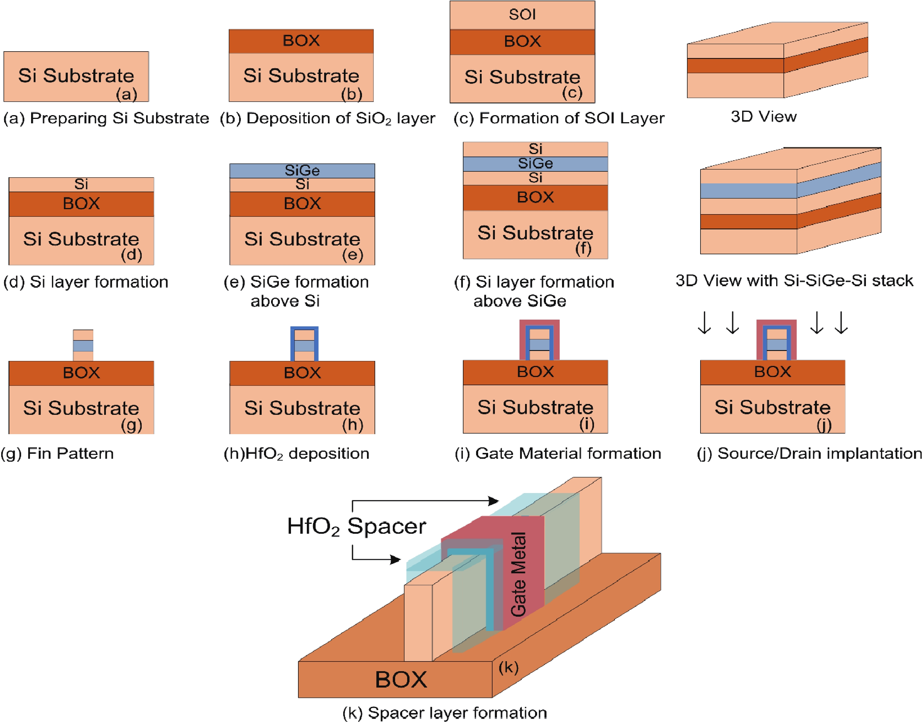
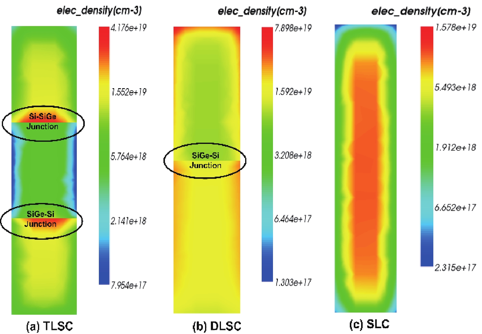
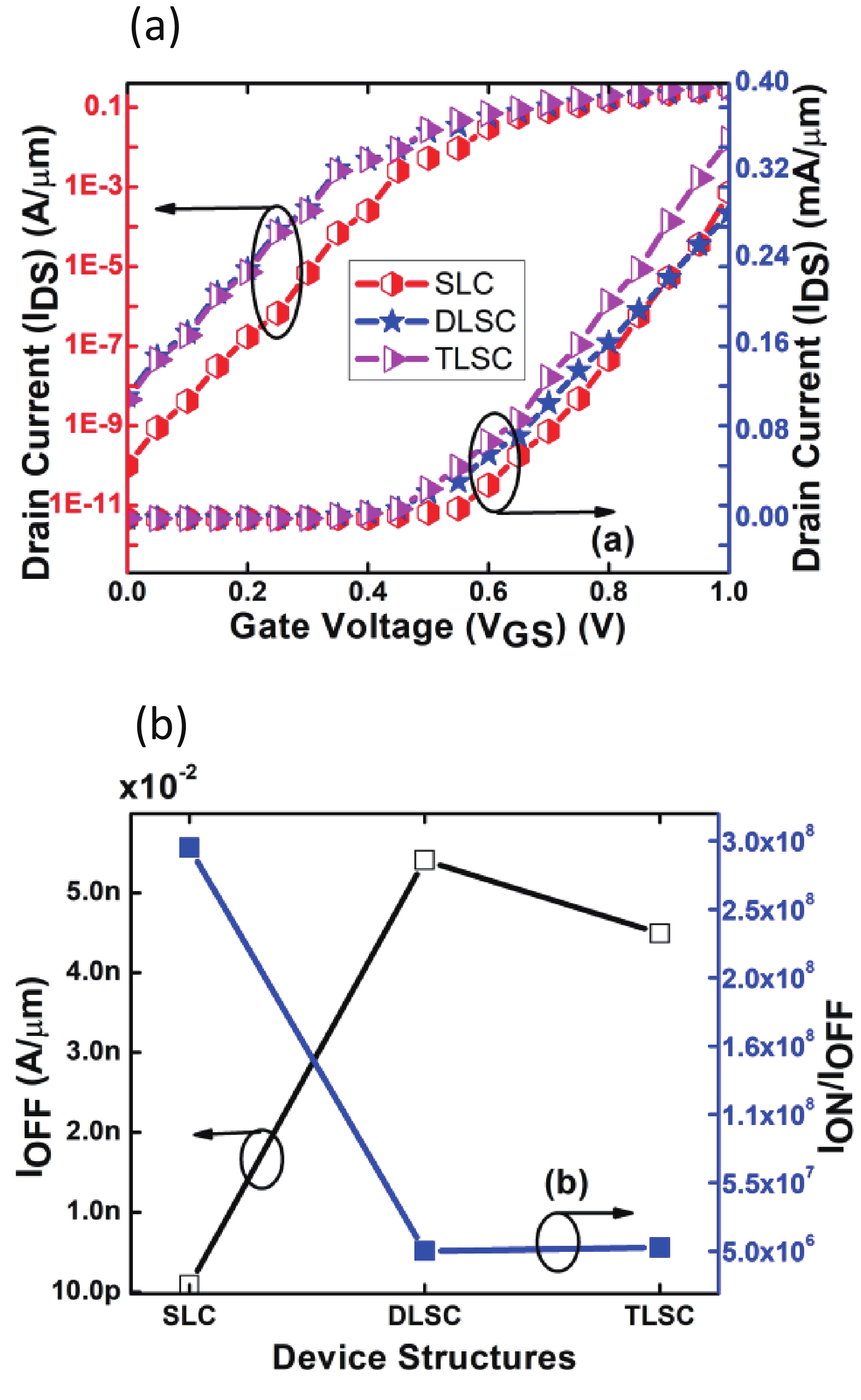
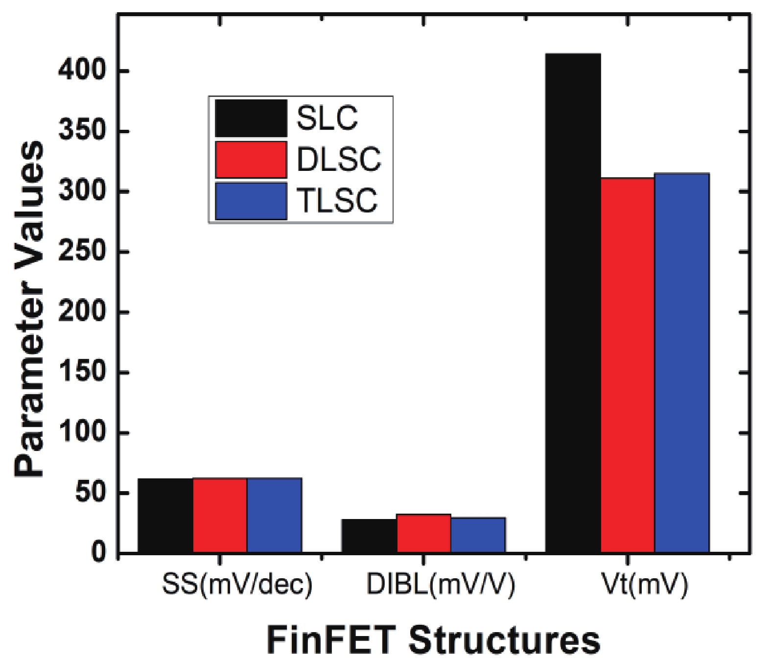
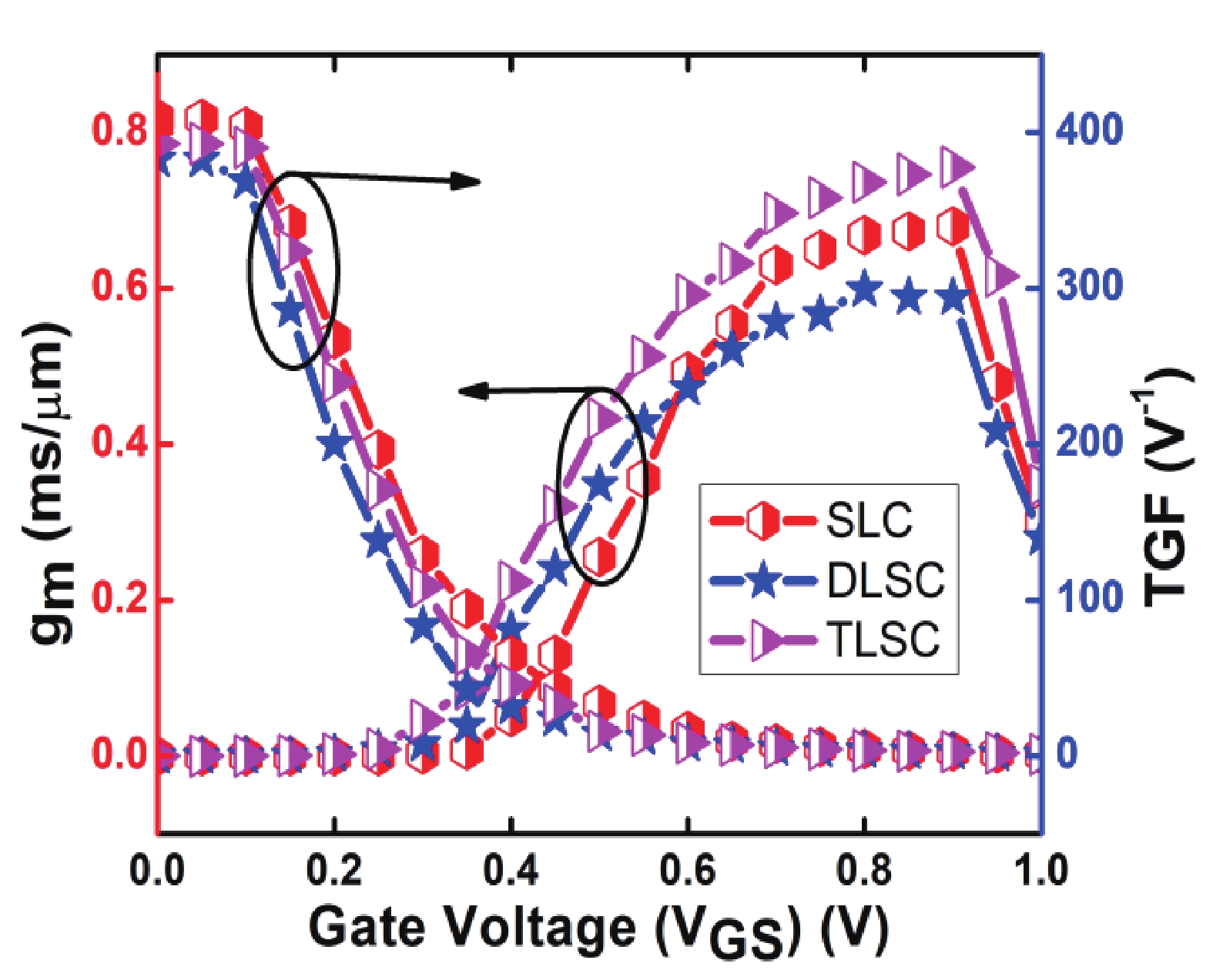
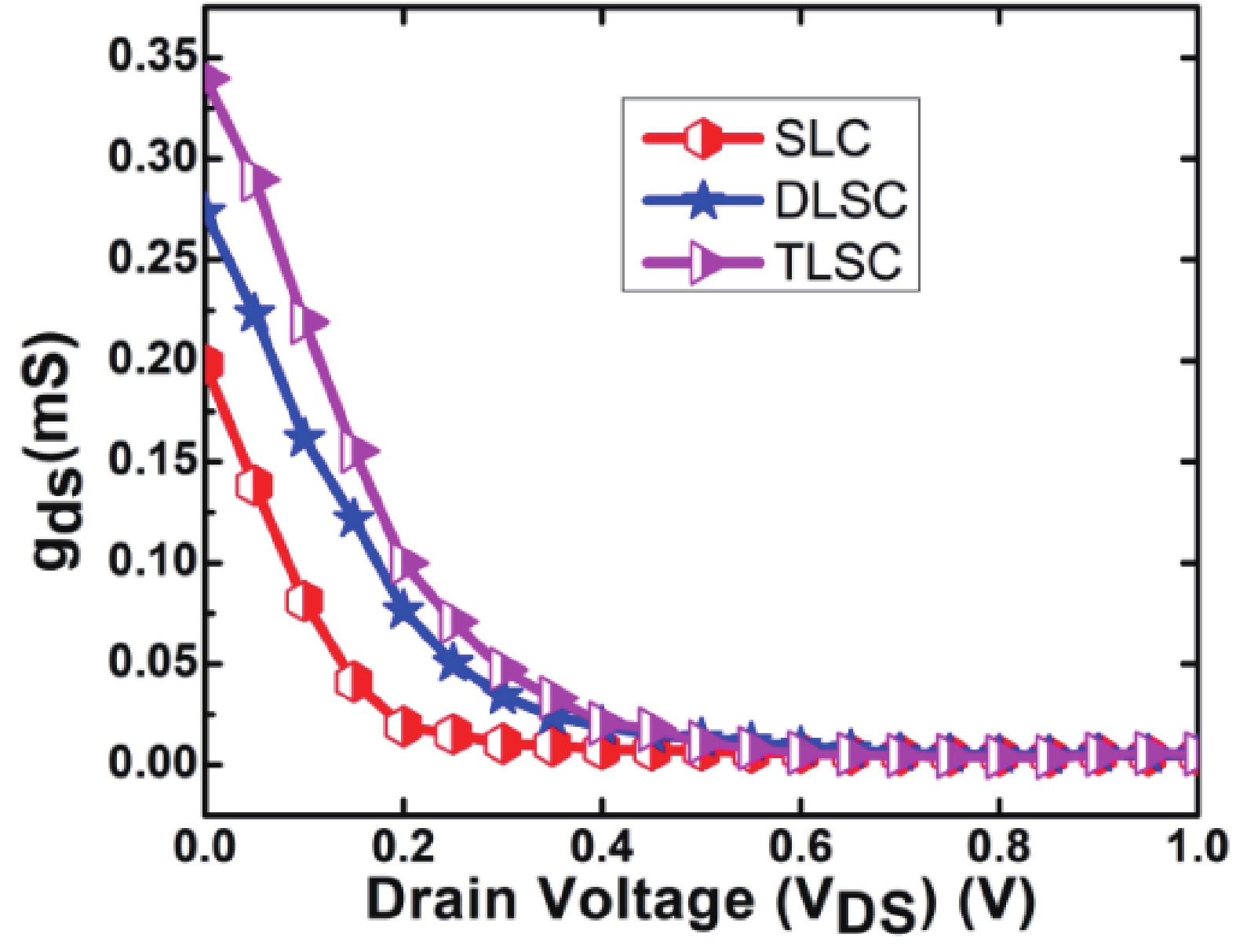
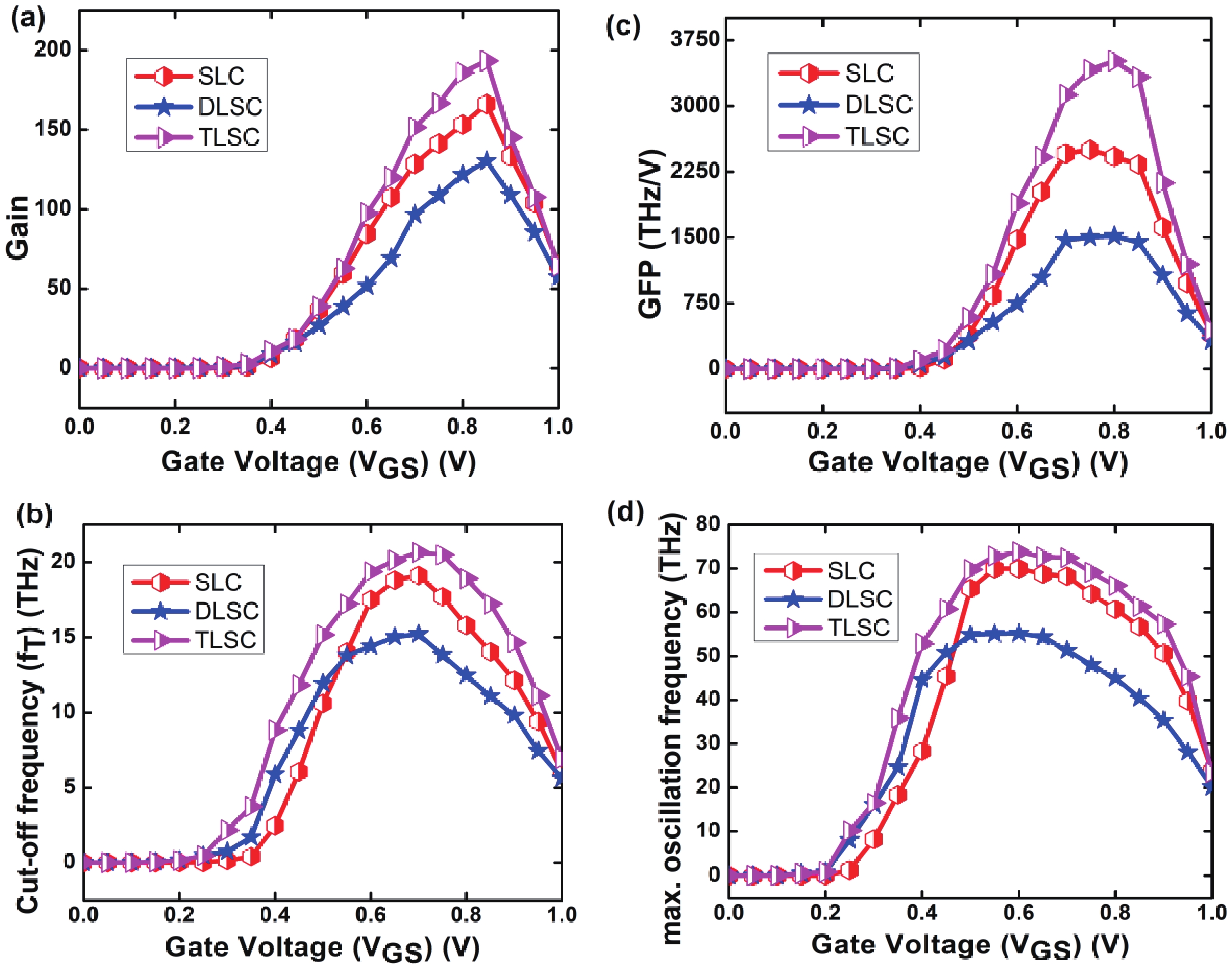
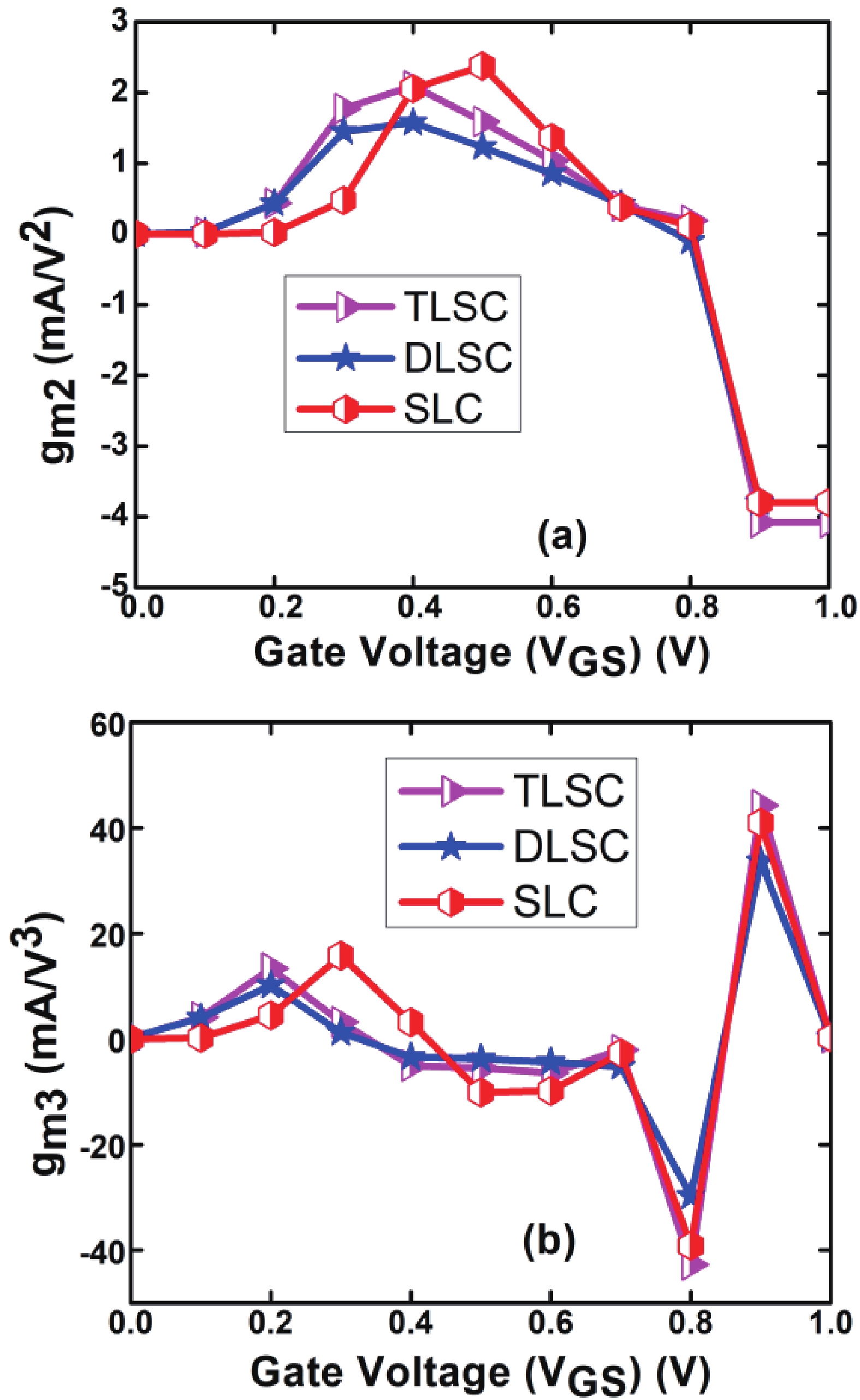
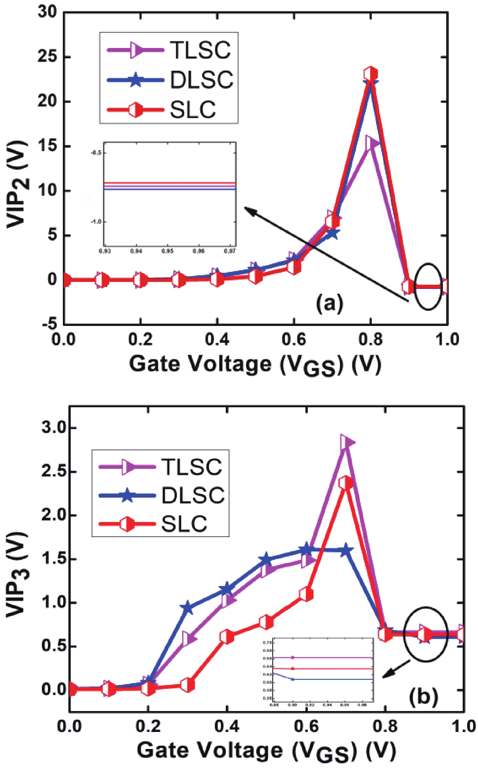
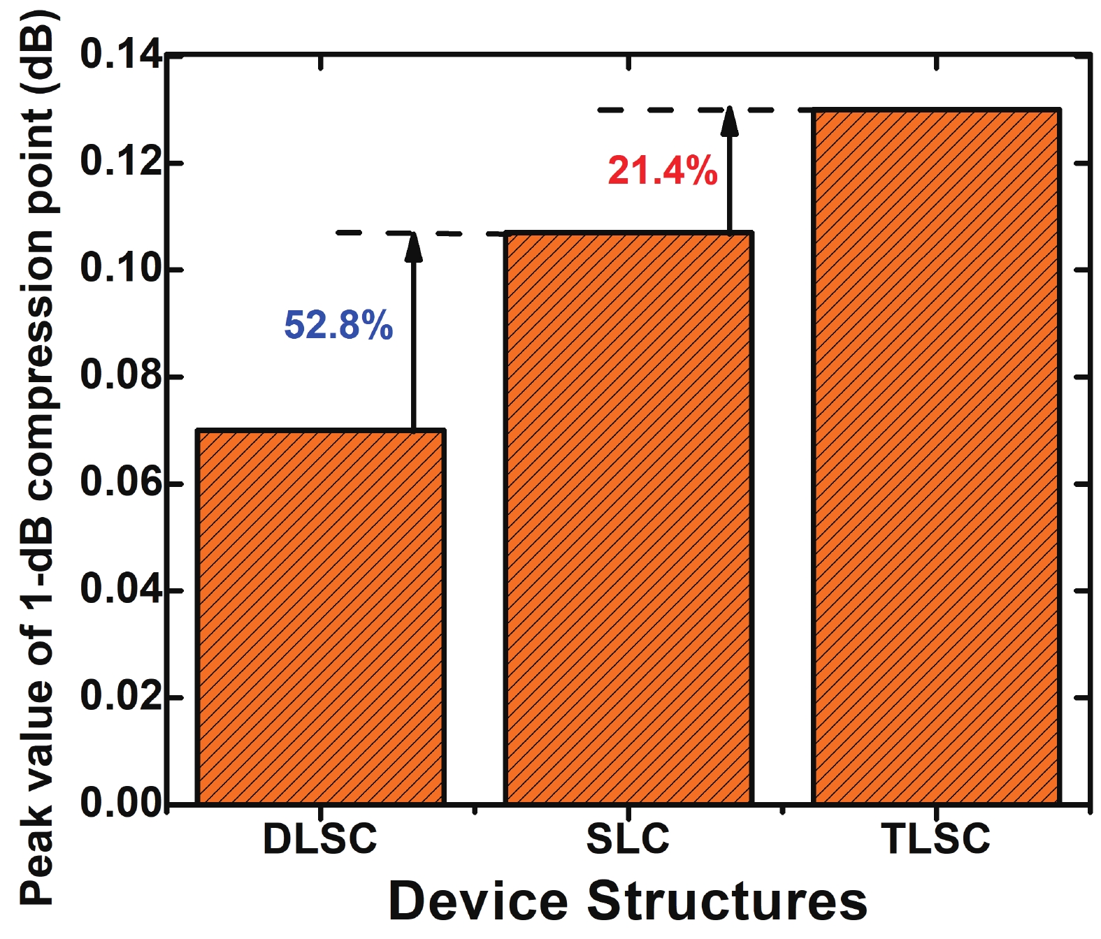
Table 1. Parameters and dimensions used for simulation.
| Device structures | |||
| Tri layer stack channel (TLSC) | Double layer stack channel (DLSC) | Single layer channel (SLC) | |
| Source/Drain material | Si | Si | Si |
| Gate length (LG) (nm) | 20 | 20 | 20 |
| Source/Drain length (LS/D) (nm) | 30 | 30 | 30 |
| Channel material | Si + Si0.75Ge0.25+Si | Si + Si0.75Ge0.25 | Si |
| Spacer material | HfO2 | HfO2 | HfO2 |
| Spacer length (LSP) (nm) | 7 | 7 | 7 |
| Total Fin height (HFin) (nm) | 36 | 36 | 36 |
| Height of each layer (nm) | 12 | 18 | 36 |
| Fin thickness (TFin) (nm) | 7 | 7 | 7 |
 DownLoad: CSV
Table 2. Summary of parameters of three junctionless structures in terms of ION, IOFF, ION/IOFF, SS, DIBL and Vt.
| Parameters | TLSC (This work) |
DLSC (This work) |
SLC (This work) |
Junctionless accumulation mode FinFET[23] |
Junctionless FinFET[24] | Junctionless bulk FinFET[25] |
| Gate length (LG) (nm) | 20 | 20 | 20 | 20 | 20 | 20 |
| Fin height (HFin) (nm) | 36 | 36 | 36 | 10 | 10 | 20 |
| Channel doping (cm−3) | 1 × 10¹⁹ | 1 × 10¹⁹ | 1 × 10¹⁹ | 5 × 10¹⁷ | 2.7 × 10¹⁹ | 1 × 10¹⁸ |
| ION (mA/µm) | 0.342 | 0.280 | 0.299 | 0.1 | 0.39 | 0.18 |
| IOFF(A/µm) (× 10−2) | 4.5 × 10⁻⁹ | 5.42 × 10⁻⁹ | 9.88 × 10⁻¹¹ | 1 × 10⁻¹⁰ | − | 1.45 × 10⁻¹⁰ |
| ION/IOFF | 7.6 × 10⁶ | 5 × 10⁶ | 3 × 10⁸ | 1 × 10⁶ | − | 1.2 × 10⁶ |
| SS (mV/dec) (VDS = 0.05 V) | 62.67 | 62.76 | 61.94 | − | − | − |
| SS (mV/dec) (VDS = 0.7 V) | 62.29 | 62.34 | 61.64 | 66 | 67.3 | 78 |
| DIBL (mV/V) | 29.6 | 32.2 | 28.07 | − | 56 | 42 |
| Vt (V) (VDS = 0.05 V) | 0.334 | 0.332 | 0.433 | |||
| Vt (V) (VDS = 0.7 V) | 0.315 | 0.317 | 0.413 | 0.25 | 0.3 | 0.15 |
DownLoad: CSV
Table 3. RF and analog parameter comparison of different structures at 20 nm gate length.
| Parameter (Peak values) |
TLSC (This work) |
DLSC (This work) |
SLC (This work) |
Junctionless FinFET[27] | Junctionless verticle super-thin body FET[28] |
Gaussian doped- junctionless FinFET[29] |
| gm (mS) | 0.75 | 0.58 | 0.67 | 0.062 | 0.067 | 0.25 |
| TGF (V−1) | 392.8 | 391.7 | 408.9 | − | − | − |
| gds (mS) | 0.339 | 0.273 | 0.198 | − | − | − |
| fT (THz) | 20.5 | 15.2 | 19.11 | 0.140 | 0.285 | 9.13 |
| fmax (THz) | 73.82 | 69.93 | 55.16 | − | − | − |
| Gain | 193.36 | 130.26 | 166.23 | − | − | − |
DownLoad: CSV
| [1] |
Hu C M. Device challenges and opportunities. Digest of Technical Papers, 2004 Symposium on VLSI Technology, 2004, 4 doi: 10.1109/VLSIT.2004.1345359
|
| [2] |
Skotnicki T, Hutchby J A, King T J, et al. The end of CMOS scaling: Toward the introduction of new materials and structural changes to improve MOSFET performance. IEEE Circuits Devices Mag, 2005, 21, 16 doi: 10.1109/MCD.2005.1388765
|
| [3] |
Bhattacharya D, Jha N K. FinFETs: From devices to architectures. Adv Electron, 2014, 2014, 1 doi: 10.1155/2014/365689
|
| [4] |
Bulusu A, Dasgupta S. Insights into channel potentials and electron quasi-Fermi potentials for DG tunnel FETs. J Semicond, 2015, 36, 014005 doi: 10.1088/1674-4926/36/1/014005
|
| [5] |
Narendar V, Mishra R A. Analytical modeling and simulation of multigate FinFET devices and the impact of high-k dielectrics on short channel effects (SCEs). Superlattices Microstruct, 2015, 85, 357 doi: 10.1016/j.spmi.2015.06.004
|
| [6] |
Yeh M S, Wu Y C, Hung M F, et al. Fabrication, characterization and simulation of Ω-gate twin poly-Si FinFET nonvolatile memory. Nanoscale Res Lett, 2013, 8, 331 doi: 10.1186/1556-276X-8-331
|
| [7] |
Leung G, Chui C O. Variability of inversion-mode and junctionless FinFETs due to line edge roughness. IEEE Electron Device Lett, 2011, 32, 1489 doi: 10.1109/LED.2011.2164233
|
| [8] |
Colinge J P, Lee C W, Afzalian A, et al. Nanowire transistors without junctions. Nature Nanotech, 2010, 5, 225 doi: 10.1038/nnano.2010.15
|
| [9] |
Liu X, Wu M L, Jin X S, et al. The optimal design of 15 nm gate-length junctionless SOI FinFETs for reducing leakage current. Semicond Sci Technol, 2013, 28, 105013 doi: 10.1088/0268-1242/28/10/105013
|
| [10] |
Chang W T, Lin Y S, Shih C T. Threshold voltage and transconductance shifting reliance on strained-SiGe channel dimension. Solid State Electron, 2015, 110, 10 doi: 10.1016/j.sse.2014.11.012
|
| [11] |
Das R, Goswami R, Baishya S. Tri-gate heterojunction SOI Ge-FinFETs. Superlattices Microstruct, 2016, 91, 51 doi: 10.1016/j.spmi.2015.12.039
|
| [12] |
Kumar M J, Venkataraman V, Nawal S. Impact of strain or Ge content on the threshold voltage of nanoscale strained-Si/SiGe bulk MOSFETs. IEEE Trans Device Mater Reliab, 2007, 7, 181 doi: 10.1109/TDMR.2006.889269
|
| [13] |
Singh T V, Jagadesh Kumar M. Effect of the Ge mole fraction on the formation of a conduction path in cylindrical strained-silicon-on-SiGe MOSFETs. Superlattices Microstruct, 2008, 44, 79 doi: 10.1016/j.spmi.2008.02.007
|
| [14] |
Venkataraman V, Nawal S, Kumar M J. Compact analytical threshold-voltage model of nanoscale fully depleted strained-Si on silicon–germanium-on-insu lator (SGOI) MOSFETs. IEEE Trans Electron Devices, 2007, 54, 554 doi: 10.1109/TED.2006.890369
|
| [15] |
Ding F, Wu Y T, Connelly D, et al. Simulation-based study of Si/Si0.9Ge0.1/Si hetero-channel FinFET for enhanced performance in low-power applications. IEEE Electron Device Lett, 2019, 40, 363 doi: 10.1109/LED.2019.2895323
|
| [16] |
Jaisawal R K, Rathore S, Kondekar P N, et al. Assessing the analog/RF and linearity performances of FinFET using high threshold voltage techniques. Semicond Sci Technol, 2022, 37, 055010 doi: 10.1088/1361-6641/ac6128
|
| [17] |
Ghosh D, Kranti Abhinav. Impact of channel doping and spacer architecture on analog/RF perfromance of lower power junctionless MOSFETs . Semicond Sci Technol, 2015, 30, 015002 doi: 10.1088/0268-1242/30/1/015002
|
| [18] |
Genius C. A CMOS TCAD Simulation Tool, User's Guide.
|
| [19] |
Rios R, Cappellani A, Armstrong M, et al. Comparison of junctionless and conventional trigate transistors with Lg down to 26 nm. IEEE Electron Device Lett, 2011, 32, 1170 doi: 10.1109/LED.2011.2158978
|
| [20] |
Colinge J P. FinFETs and other multi-gate transistors. Springer, 2008
|
| [21] |
Badaroglu M. More Moore. 2021 IEEE International Roadmap for Devices and Systems Outbriefs, 2022, 1
|
| [22] |
Rahimian M, Orouji A A, Aminbeidokhti A. A novel deep submicron SiGe-on-insulator (SGOI) MOSFET with modified channel band energy for electrical performance improvement. Curr Appl Phys, 2013, 13, 779 doi: 10.1016/j.cap.2012.12.005
|
| [23] |
Hu L D, Lou H J, Li W T, et al. Suppression of statistical variability in junctionless FinFET using accumulation-mode and charge plasma structure. IEEE Trans Electron Devices, 2021, 68, 399 doi: 10.1109/TED.2020.3040137
|
| [24] |
Seo J H, Yuan H, Kang I M. Design optimization of silicon-based junctionless fin-type field-effect transistors for low standby power technology. J Electr Eng Technol, 2013, 8, 1497 doi: 10.5370/JEET.2013.8.6.1497
|
| [25] |
Biswas K, Sarkar A, Sarkar C K. Linearity and analog performance analysis of silicon junctionless bulk FinFET considering gate electrode workfunction variability and different fin aspect ratio. Silicon, 2022, 14, 7531 doi: 10.1007/s12633-021-01513-6
|
| [26] |
Srivastava N A, Priya A, Mishra R A. Analog and radio-frequency performance of nanoscale SOI MOSFET for RFIC based communication systems. Microelectron J, 2020, 98, 104731 doi: 10.1016/j.mejo.2020.104731
|
| [27] |
Jegadheesan V, Sivasankaran K. RF stability performance of SOI junctionless FinFET and impact of process variation. Microelectron J, 2017, 59, 15 doi: 10.1016/j.mejo.2016.11.004
|
| [28] |
Barman K R, Baishya S. An insight into the DC and analog/RF response of a junctionless vertical super-thin body FET towards high-K gate dielectrics. Silicon, 2022, 14, 6113 doi: 10.1007/s12633-021-01393-w
|
| [29] |
Manikandan S, Balamurugan N B. The improved RF/stability and linearity performance of the ultrathin-body Gaussian-doped junctionless FinFET. J Comput Electron, 2020, 19, 613 doi: 10.1007/s10825-020-01472-y
|
| [30] |
Schwierz F, Liou J J. Semiconductor devices for RF applications: Evolution and current status. Microelectron Reliab, 2001, 41, 145 doi: 10.1016/S0026-2714(00)00076-7
|
| [31] |
Sarkar A, Kumar Das A, De S, et al. Effect of gate engineering in double-gate MOSFETs for analog/RF applications. Microelectron J, 2012, 43, 873 doi: 10.1016/j.mejo.2012.06.002
|


Article views: 2874 Times PDF downloads: 227 Times Cited by: 0 Times
Received: 11 February 2023 Revised: 03 March 2023 Online: Accepted Manuscript: 31 August 2023Corrected proof: 18 October 2023Uncorrected proof: 20 October 2023Published: 10 November 2023
| Citation: |
Devenderpal Singh, Shalini Chaudhary, Basudha Dewan, Menka Yadav. Performance optimization of tri-gate junctionless FinFET using channel stack engineering for digital and analog/RF design[J]. Journal of Semiconductors, 2023, 44(11): 114103. doi: 10.1088/1674-4926/44/11/114103
****
D Singh, S Chaudhary, B Dewan, M Yadav. Performance optimization of tri-gate junctionless FinFET using channel stack engineering for digital and analog/RF design[J]. J. Semicond, 2023, 44(11): 114103. doi: 10.1088/1674-4926/44/11/114103

|
 Devenderpal Singh:completed M.Tech degree in VLSI Design and CAD from Thapar University, India in 2013. He has worked as a Research Associate at IIT Jodhpur and Assistant Professor at Chitkara University, Chandigarh, India, during 2014−2019. He is currently pursuing Ph.D in the Department of Electronics and Communication Engineering from Malaviya National Institute of Technology, Jaipur, India. His research interests include Microelectronic device modeling and simulation, SRAM design, Compute-In-Memory
 Shalini Chaudhary:received M.Tech degree in VLSI designing from the Banasthali University, India. She is currently pursuing Ph.D degree in Department of Electronics and Communication Engineering from Malaviya National Institute of Technology, Jaipur, India. Her research interests include micro and nano-electronic device modeling and simulation
 Basudha Dewan:received M.Tech degree in Electronics and Communication Engineering from Punjab Engineering College (PEC), Chandigarh, India, in 2018. She is currently pursuing Ph.D in the Department of Electronics and Communication Engineering from Malaviya National Institute of Technology, Jaipur, India. Her research intersets include modeling and simulation of advanced semiconductor devices, design and development of semiconducotr based hybrid sensor systems
 Menka Yadav:has completed her B.E. from Government Engineering College Ajmer in 2006, M.Tech from MNIT Jaipur in 2008 and Ph.D from IIT Roorkee in 2016. She has worked at BML University Gurugram, NIT Tiruchirappalli before joining MNIT Jaipur in 2019. Her research interest is device design and modeling. Applications of emerging devices to digital, analog and sensor domain, Solar cell etc
| [1] |
Hu C M. Device challenges and opportunities. Digest of Technical Papers, 2004 Symposium on VLSI Technology, 2004, 4 doi: 10.1109/VLSIT.2004.1345359
|
| [2] |
Skotnicki T, Hutchby J A, King T J, et al. The end of CMOS scaling: Toward the introduction of new materials and structural changes to improve MOSFET performance. IEEE Circuits Devices Mag, 2005, 21, 16 doi: 10.1109/MCD.2005.1388765
|
| [3] |
Bhattacharya D, Jha N K. FinFETs: From devices to architectures. Adv Electron, 2014, 2014, 1 doi: 10.1155/2014/365689
|
| [4] |
Bulusu A, Dasgupta S. Insights into channel potentials and electron quasi-Fermi potentials for DG tunnel FETs. J Semicond, 2015, 36, 014005 doi: 10.1088/1674-4926/36/1/014005
|
| [5] |
Narendar V, Mishra R A. Analytical modeling and simulation of multigate FinFET devices and the impact of high-k dielectrics on short channel effects (SCEs). Superlattices Microstruct, 2015, 85, 357 doi: 10.1016/j.spmi.2015.06.004
|
| [6] |
Yeh M S, Wu Y C, Hung M F, et al. Fabrication, characterization and simulation of Ω-gate twin poly-Si FinFET nonvolatile memory. Nanoscale Res Lett, 2013, 8, 331 doi: 10.1186/1556-276X-8-331
|
| [7] |
Leung G, Chui C O. Variability of inversion-mode and junctionless FinFETs due to line edge roughness. IEEE Electron Device Lett, 2011, 32, 1489 doi: 10.1109/LED.2011.2164233
|
| [8] |
Colinge J P, Lee C W, Afzalian A, et al. Nanowire transistors without junctions. Nature Nanotech, 2010, 5, 225 doi: 10.1038/nnano.2010.15
|
| [9] |
Liu X, Wu M L, Jin X S, et al. The optimal design of 15 nm gate-length junctionless SOI FinFETs for reducing leakage current. Semicond Sci Technol, 2013, 28, 105013 doi: 10.1088/0268-1242/28/10/105013
|
| [10] |
Chang W T, Lin Y S, Shih C T. Threshold voltage and transconductance shifting reliance on strained-SiGe channel dimension. Solid State Electron, 2015, 110, 10 doi: 10.1016/j.sse.2014.11.012
|
| [11] |
Das R, Goswami R, Baishya S. Tri-gate heterojunction SOI Ge-FinFETs. Superlattices Microstruct, 2016, 91, 51 doi: 10.1016/j.spmi.2015.12.039
|
| [12] |
Kumar M J, Venkataraman V, Nawal S. Impact of strain or Ge content on the threshold voltage of nanoscale strained-Si/SiGe bulk MOSFETs. IEEE Trans Device Mater Reliab, 2007, 7, 181 doi: 10.1109/TDMR.2006.889269
|
| [13] |
Singh T V, Jagadesh Kumar M. Effect of the Ge mole fraction on the formation of a conduction path in cylindrical strained-silicon-on-SiGe MOSFETs. Superlattices Microstruct, 2008, 44, 79 doi: 10.1016/j.spmi.2008.02.007
|
| [14] |
Venkataraman V, Nawal S, Kumar M J. Compact analytical threshold-voltage model of nanoscale fully depleted strained-Si on silicon–germanium-on-insu lator (SGOI) MOSFETs. IEEE Trans Electron Devices, 2007, 54, 554 doi: 10.1109/TED.2006.890369
|
| [15] |
Ding F, Wu Y T, Connelly D, et al. Simulation-based study of Si/Si0.9Ge0.1/Si hetero-channel FinFET for enhanced performance in low-power applications. IEEE Electron Device Lett, 2019, 40, 363 doi: 10.1109/LED.2019.2895323
|
| [16] |
Jaisawal R K, Rathore S, Kondekar P N, et al. Assessing the analog/RF and linearity performances of FinFET using high threshold voltage techniques. Semicond Sci Technol, 2022, 37, 055010 doi: 10.1088/1361-6641/ac6128
|
| [17] |
Ghosh D, Kranti Abhinav. Impact of channel doping and spacer architecture on analog/RF perfromance of lower power junctionless MOSFETs . Semicond Sci Technol, 2015, 30, 015002 doi: 10.1088/0268-1242/30/1/015002
|
| [18] |
Genius C. A CMOS TCAD Simulation Tool, User's Guide.
|
| [19] |
Rios R, Cappellani A, Armstrong M, et al. Comparison of junctionless and conventional trigate transistors with Lg down to 26 nm. IEEE Electron Device Lett, 2011, 32, 1170 doi: 10.1109/LED.2011.2158978
|
| [20] |
Colinge J P. FinFETs and other multi-gate transistors. Springer, 2008
|
| [21] |
Badaroglu M. More Moore. 2021 IEEE International Roadmap for Devices and Systems Outbriefs, 2022, 1
|
| [22] |
Rahimian M, Orouji A A, Aminbeidokhti A. A novel deep submicron SiGe-on-insulator (SGOI) MOSFET with modified channel band energy for electrical performance improvement. Curr Appl Phys, 2013, 13, 779 doi: 10.1016/j.cap.2012.12.005
|
| [23] |
Hu L D, Lou H J, Li W T, et al. Suppression of statistical variability in junctionless FinFET using accumulation-mode and charge plasma structure. IEEE Trans Electron Devices, 2021, 68, 399 doi: 10.1109/TED.2020.3040137
|
| [24] |
Seo J H, Yuan H, Kang I M. Design optimization of silicon-based junctionless fin-type field-effect transistors for low standby power technology. J Electr Eng Technol, 2013, 8, 1497 doi: 10.5370/JEET.2013.8.6.1497
|
| [25] |
Biswas K, Sarkar A, Sarkar C K. Linearity and analog performance analysis of silicon junctionless bulk FinFET considering gate electrode workfunction variability and different fin aspect ratio. Silicon, 2022, 14, 7531 doi: 10.1007/s12633-021-01513-6
|
| [26] |
Srivastava N A, Priya A, Mishra R A. Analog and radio-frequency performance of nanoscale SOI MOSFET for RFIC based communication systems. Microelectron J, 2020, 98, 104731 doi: 10.1016/j.mejo.2020.104731
|
| [27] |
Jegadheesan V, Sivasankaran K. RF stability performance of SOI junctionless FinFET and impact of process variation. Microelectron J, 2017, 59, 15 doi: 10.1016/j.mejo.2016.11.004
|
| [28] |
Barman K R, Baishya S. An insight into the DC and analog/RF response of a junctionless vertical super-thin body FET towards high-K gate dielectrics. Silicon, 2022, 14, 6113 doi: 10.1007/s12633-021-01393-w
|
| [29] |
Manikandan S, Balamurugan N B. The improved RF/stability and linearity performance of the ultrathin-body Gaussian-doped junctionless FinFET. J Comput Electron, 2020, 19, 613 doi: 10.1007/s10825-020-01472-y
|
| [30] |
Schwierz F, Liou J J. Semiconductor devices for RF applications: Evolution and current status. Microelectron Reliab, 2001, 41, 145 doi: 10.1016/S0026-2714(00)00076-7
|
| [31] |
Sarkar A, Kumar Das A, De S, et al. Effect of gate engineering in double-gate MOSFETs for analog/RF applications. Microelectron J, 2012, 43, 873 doi: 10.1016/j.mejo.2012.06.002
|

 WeChat ID
Journal of Semiconductors © 2017 All Rights Reserved 京ICP备05085259号-2


