


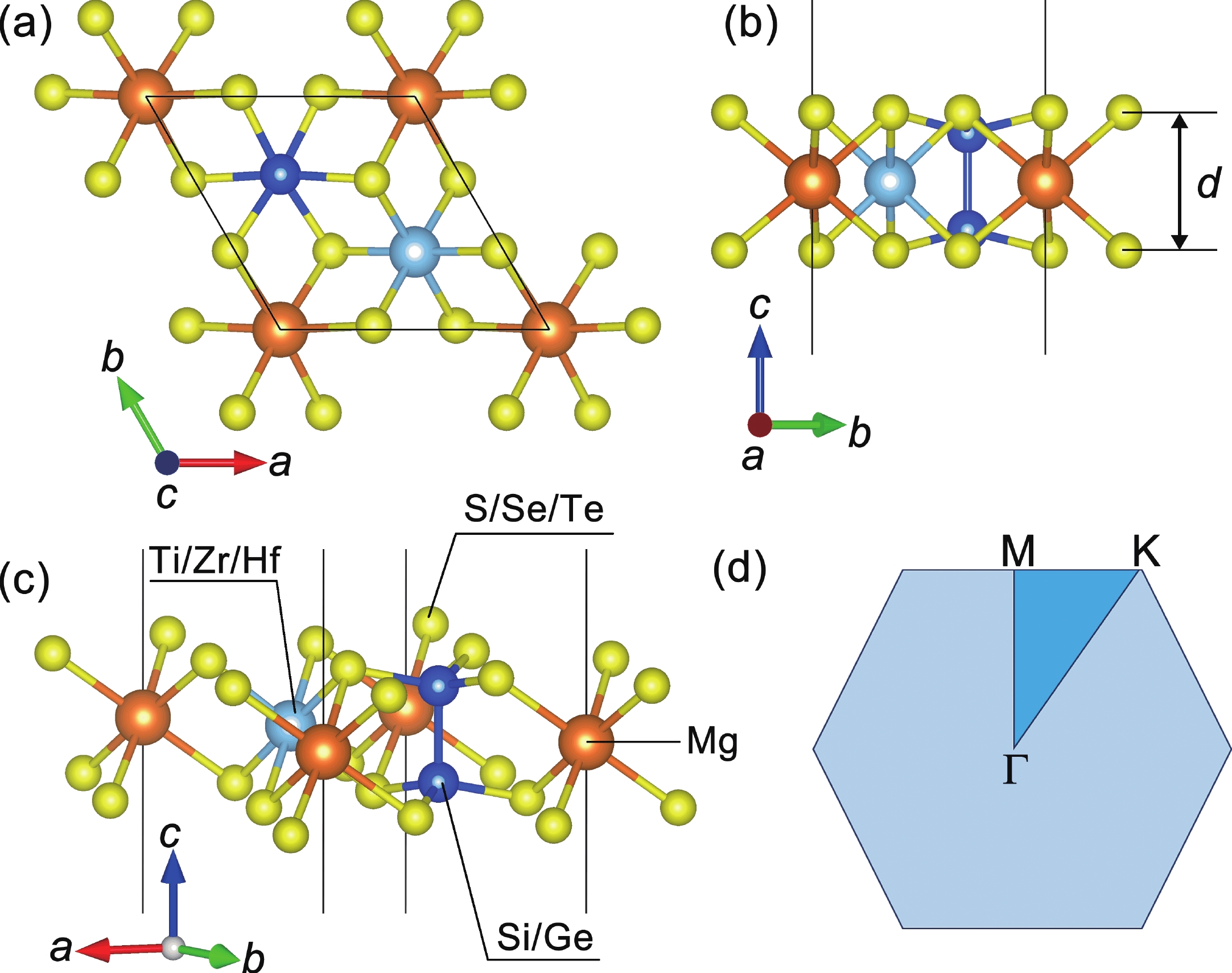
Fig. 1.
(Color online) (a) The top view and (b, c) side view of monolayer MgMX2Y6. (d) The corresponding first Brillouin zone of MgMX2Y6 monolayers.
ARTICLES
Junhui Yuan1, Kanhao Xue1, 2, , Xiangshui Miao1, 2 and Lei Ye1, 2,
Corresponding author: Kanhao Xue, xkh@hust.edu.cn; Lei Ye, leiye@hust.edu.cn
Abstract: Inspired by the recently predicted 2D MX2Y6 (M = metal element; X = Si/Ge/Sn; Y = S/Se/Te), we explore the possible applications of alkaline earth metal (using magnesium as example) in this family based on the idea of element replacement and valence electron balance. Herein, we report a new family of 2D quaternary compounds, namely MgMX2Y6 (M = Ti/Zr/Hf; X = Si/Ge; Y = S/Se/Te) monolayers, with superior kinetic, thermodynamic and mechanical stability. In addition, our results indicate that MgMX2Y6 monolayers are all indirect band gap semiconductors with band gap values ranging from 0.870 to 2.500 eV. Moreover, the band edges and optical properties of 2D MgMX2Y6 are suitable for constructing multifunctional optoelectronic devices. Furthermore, for comparison, the mechanical, electronic and optical properties of In2X2Y6 monolayers have been discussed in detail. The success of introducing Mg into the 2D MX2Y6 family indicates that more potential materials, such as Ca- and Sr-based 2D MX2Y6 monolayers, may be discovered in the future. Therefore, this work not only broadens the existing family of 2D semiconductors, but it also provides beneficial results for the future.
Keywords: two-dimensional materials, MgMX2Y6 monolayer, In2X2Y6 monolayer, semiconductor, first-principles calculations
| [1] |
Novoselov K S, Geim A K, Morozov S V, et al. Electric field effect in atomically thin carbon films. Science, 2004, 306, 666 doi: 10.1126/science.1102896
|
| [2] |
Akinwande D, Huyghebaert C, Wang C H, et al. Graphene and two-dimensional materials for silicon technology. Nature, 2019, 573, 507 doi: 10.1038/s41586-019-1573-9
|
| [3] |
Yuan J H, Yu N N, Xue K H, et al. Ideal strength and elastic instability in single-layer 8-Pmmn borophene. RSC Adv, 2017, 7, 8654 doi: 10.1039/C6RA28454J
|
| [4] |
Yuan J H, Yu N N, Xue K H, et al. Stability, electronic and thermodynamic properties of aluminene from first-principles calculations. Appl Surf Sci, 2017, 409, 85 doi: 10.1016/j.apsusc.2017.02.238
|
| [5] |
Balendhran S, Walia S, Nili H, et al. Elemental analogues of graphene: Silicene, germanene, stanene, and phosphorene. Small, 2015, 11, 640 doi: 10.1002/smll.201402041
|
| [6] |
Yuan P W, Zhang T, Sun J T, et al. Recent progress in 2D group-V elemental monolayers: Fabrications and properties. J Semicond, 2020, 41, 081003 doi: 10.1088/1674-4926/41/8/081003
|
| [7] |
Wang Y X, Qiu G, Wang R X, et al. Field-effect transistors made from solution-grown two-dimensional tellurene. Nat Electron, 2018, 1, 228 doi: 10.1038/s41928-018-0058-4
|
| [8] |
Liu Y, Duan X D, Huang Y, et al. Two-dimensional transistors beyond graphene and TMDCs. Chem Soc Rev, 2018, 47, 6388 doi: 10.1039/C8CS00318A
|
| [9] |
Tong L, Peng Z R, Lin R F, et al. 2D materials-based homogeneous transistor-memory architecture for neuromorphic hardware. Science, 2021, 373, 1353 doi: 10.1126/science.abg3161
|
| [10] |
Morales-García Á, Calle-Vallejo F, Illas F. MXenes: New horizons in catalysis. ACS Catal, 2020, 10, 13487 doi: 10.1021/acscatal.0c03106
|
| [11] |
Wang L, Shi Y P, Liu M F, et al. Intercalated architecture of MA2Z4 family layered van der Waals materials with emerging topological, magnetic and superconducting properties. Nat Commun, 2021, 12, 2361 doi: 10.1038/s41467-021-22324-8
|
| [12] |
Ding W J, Zhu J B, Wang Z, et al. Prediction of intrinsic two-dimensional ferroelectrics in In2Se3 and other III2-VI3 van der Waals materials. Nat Commun, 2017, 8, 14956 doi: 10.1038/ncomms14956
|
| [13] |
Deng J, Deng D H, Bao X H. Robust catalysis on 2D materials encapsulating metals: Concept, application, and perspective. Adv Mater, 2017, 29, 1606967 doi: 10.1002/adma.201606967
|
| [14] |
Lemme M C, Akinwande D, Huyghebaert C, et al. 2D materials for future heterogeneous electronics. Nat Commun, 2022, 13, 1392 doi: 10.1038/s41467-022-29001-4
|
| [15] |
Tang K, Wang Y, Gong C H, et al. Electronic and photoelectronic memristors based on 2D materials. Adv Elect Mater, 2022, 8, 2101099 doi: 10.1002/aelm.202101099
|
| [16] |
Anichini C, Czepa W, Pakulski D, et al. Chemical sensing with 2D materials. Chem Soc Rev, 2018, 47, 4860 doi: 10.1039/C8CS00417J
|
| [17] |
Wu F, Tian H, Shen Y, et al. Vertical MoS2 transistors with sub-1-nm gate lengths. Nature, 2022, 603, 259 doi: 10.1038/s41586-021-04323-3
|
| [18] |
Li X F, Yu Z Q, Xiong X, et al. High-speed black phosphorus field-effect transistors approaching ballistic limit. Sci Adv, 2019, 5, eaau3194 doi: 10.1126/sciadv.aau3194
|
| [19] |
Wang Y C, Lv J, Zhu L, et al. CALYPSO: A method for crystal structure prediction. Comput Phys Commun, 2012, 183, 2063 doi: 10.1016/j.cpc.2012.05.008
|
| [20] |
Glass C W, Oganov A R, Hansen N. USPEX—Evolutionary crystal structure prediction. Comput Phys Commun, 2006, 175, 713 doi: 10.1016/j.cpc.2006.07.020
|
| [21] |
Yu W Y, Niu C Y, Zhu Z L, et al. Atomically thin binary V-V compound semiconductor: A first-principles study. J Mater Chem C, 2016, 4, 6581 doi: 10.1039/C6TC01505K
|
| [22] |
Jin X, Tao L, Zhang Y Y, et al. Intrinsically scale-free ferroelectricity in two-dimensional M2X2Y6. Nano Res, 2022, 15, 3704 doi: 10.1007/s12274-021-3919-5
|
| [23] |
Miao N H, Li W, Zhu L G, et al. Tunable phase transitions and high photovoltaic performance of two-dimensional In2Ge2Te6 semiconductors. Nanoscale Horiz, 2020, 5, 1566 doi: 10.1039/D0NH00395F
|
| [24] |
Hao K R, Ma X Y, Lyu H Y, et al. The atlas of ferroicity in two-dimensional MGeX3 family: Room-temperature ferromagnetic half metals and unexpected ferroelectricity and ferroelasticity. Nano Res, 2021, 14, 4732 doi: 10.1007/s12274-021-3415-6
|
| [25] |
Hao K R, Ma X Y, Zhang Z, et al. Ferroelectric and room-temperature ferromagnetic semiconductors in the 2D MIMIIGe2X6 family: First-principles and machine learning investigations. J Phys Chem Lett, 2021, 12, 10040 doi: 10.1021/acs.jpclett.1c02782
|
| [26] |
Nityananda R, Hohenberg P, Kohn W. Inhomogeneous electron gas. Reson, 2017, 22, 809 doi: 10.1007/s12045-017-0529-3
|
| [27] |
Blöchl P E. Projector augmented-wave method. Phys Rev B, 1994, 50, 17953 doi: 10.1103/PhysRevB.50.17953
|
| [28] |
Kresse G, Joubert D. From ultrasoft pseudopotentials to the projector augmented-wave method. Phys Rev B, 1999, 59, 1758 doi: 10.1103/PhysRevB.59.1758
|
| [29] |
Kresse G, Furthmüller J. Efficiency of ab-initio total energy calculations for metals and semiconductors using a plane-wave basis set. Comput Mater Sci, 1996, 6, 15 doi: 10.1016/0927-0256(96)00008-0
|
| [30] |
Kresse G, Furthmüller J. Efficient iterative schemes for ab initio total-energy calculations using a plane-wave basis set. Phys Rev B, 1996, 54, 11169 doi: 10.1103/PhysRevB.54.11169
|
| [31] |
Perdew J P, Burke K, Ernzerhof M. Generalized gradient approximation made simple. Phys Rev Lett, 1996, 77, 3865 doi: 10.1103/PhysRevLett.77.3865
|
| [32] |
Xue K H, Yuan J H, Fonseca L R C, et al. Improved LDA-1/2 method for band structure calculations in covalent semiconductors. Comput Mater Sci, 2018, 153, 493 doi: 10.1016/j.commatsci.2018.06.036
|
| [33] |
Yuan J H, Chen Q, Fonseca L R C, et al. GGA-1/2 self-energy correction for accurate band structure calculations: The case of resistive switching oxides. J Phys Commun, 2018, 2, 105005 doi: 10.1088/2399-6528/aade7e
|
| [34] |
Krukau A V, Vydrov O A, Izmaylov A F, et al. Influence of the exchange screening parameter on the performance of screened hybrid functionals. J Chem Phys, 2006, 125, 224106 doi: 10.1063/1.2404663
|
| [35] |
Togo A, Oba F, Tanaka I. First-principles calculations of the ferroelastic transition between rutile-type and CaCl2-type SiO2 at high pressures. Phys Rev B, 2008, 78, 134106 doi: 10.1103/PhysRevB.78.134106
|
| [36] |
Jin H, Tan X X, Wang T, et al. Discovery of two-dimensional multinary component photocatalysts accelerated by machine learning. J Phys Chem Lett, 2022, 13, 7228 doi: 10.1021/acs.jpclett.2c01862
|
| [37] |
Kamal C, Ezawa M. Arsenene: Two-dimensional buckled and puckered honeycomb arsenic systems. Phys Rev B, 2015, 91, 085423 doi: 10.1103/PhysRevB.91.085423
|
| [38] |
Liu Z, Wang H D, Sun J Y, et al. Penta-Pt2N4: An ideal two-dimensional material for nanoelectronics. Nanoscale, 2018, 10, 16169 doi: 10.1039/C8NR05561K
|
| [39] |
Yuan J H, Song Y Q, Chen Q, et al. Single-layer planar penta-X2N4 (X = Ni, Pd and Pt) as direct-bandgap semiconductors from first principle calculations. Appl Surf Sci, 2019, 469, 456 doi: 10.1016/j.apsusc.2018.11.041
|
| [40] |
Born M, Huang K. Dynamical theory of crystal lattices. Oxford: Clarendon Press, 1954
|
| [41] |
Tang W, Sanville E, Henkelman G. A grid-based Bader analysis algorithm without lattice bias. J Phys: Condens Matter, 2009, 21, 084204 doi: 10.1088/0953-8984/21/8/084204
|
| [42] |
Liu F, Ming P B, Li J. Ab initio calculation of ideal strength and phonon instability of graphene under tension. Phys Rev B, 2007, 76, 064120 doi: 10.1103/PhysRevB.76.064120
|
| [43] |
Andrew R C, Mapasha R E, Ukpong A M, et al. Mechanical properties of graphene and boronitrene. Phys Rev B, 2012, 85, 125428 doi: 10.1103/PhysRevB.85.125428
|
| [44] |
Li J W, Medhekar N V, Shenoy V B. Bonding charge density and ultimate strength of monolayer transition metal dichalcogenides. J Phys Chem C, 2013, 117, 15842 doi: 10.1021/jp403986v
|
| [45] |
Li J, Zhou W H, Xu L L, et al. Revealing the weak Fermi level pinning effect of 2D semiconductor/2D metal contact: A case of monolayer In2Ge2Te6 and its Janus structure In2Ge2Te3Se3. Mater Today Phys, 2022, 26, 100749 doi: 10.1016/j.mtphys.2022.100749
|
| [46] |
Yuan J H, Zhang B, Song Y Q, et al. Planar penta-transition metal phosphide and arsenide as narrow-gap semiconductors with ultrahigh carrier mobility. J Mater Sci, 2019, 54, 7035 doi: 10.1007/s10853-019-03380-4
|
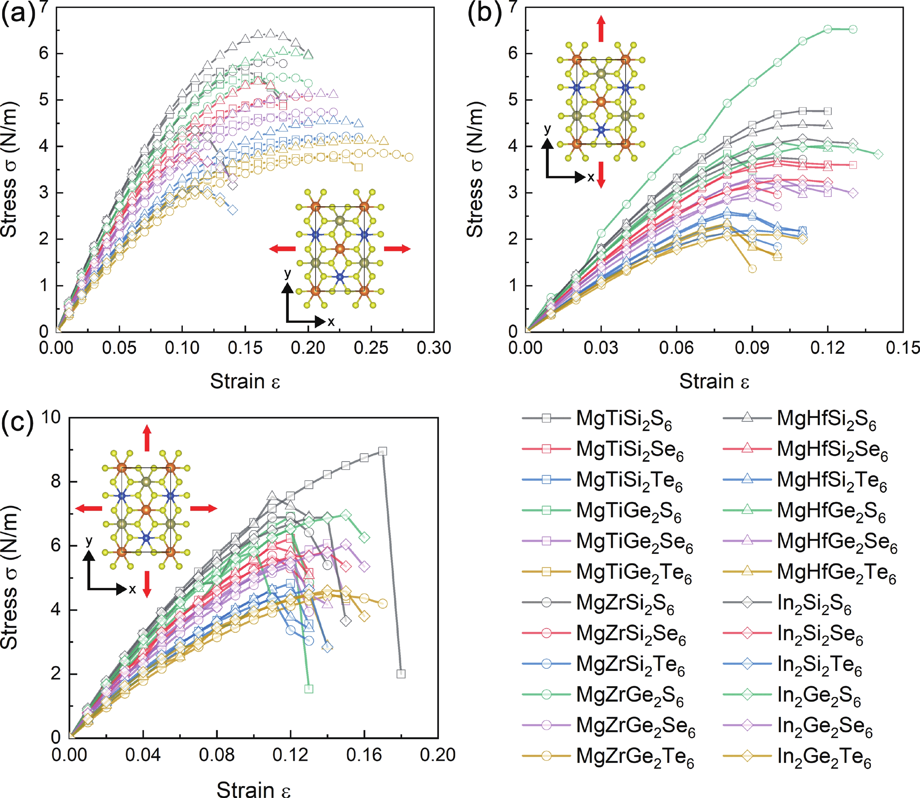
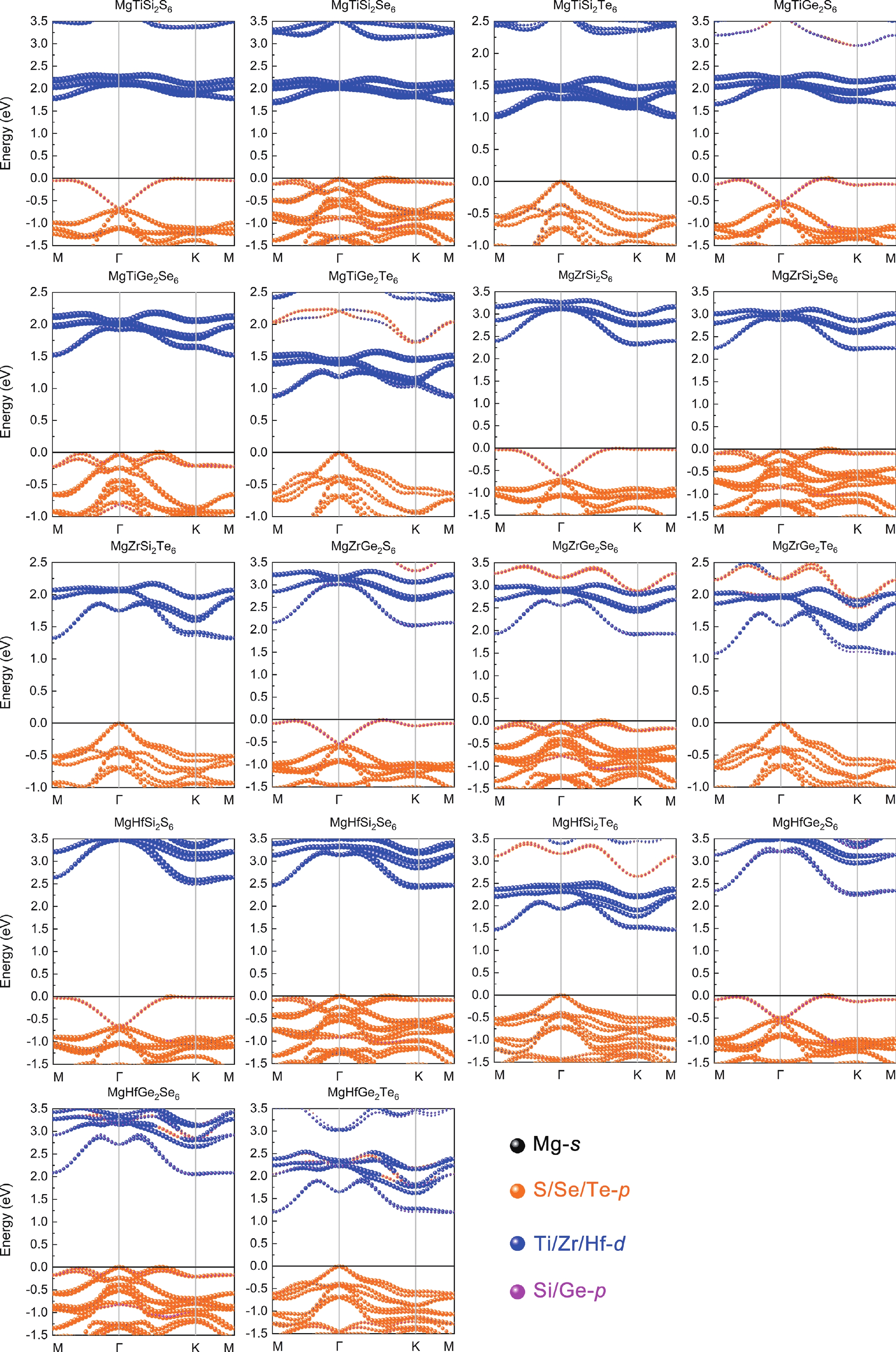
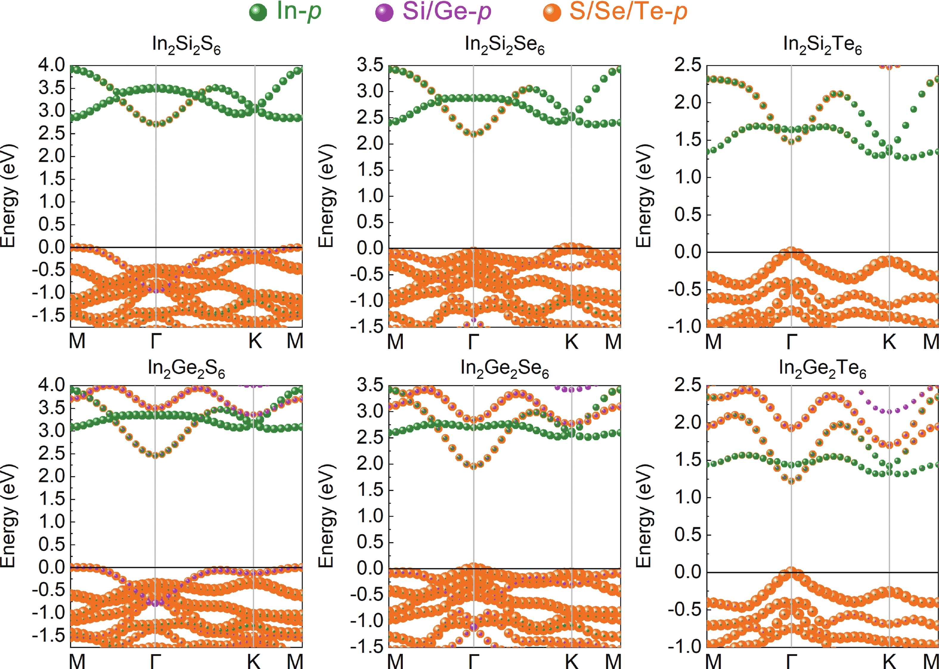
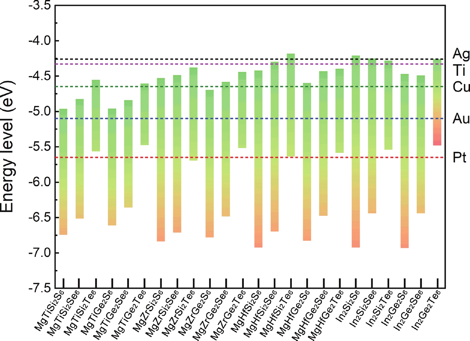
Table 1. Calculated lattice constant a/b (Å), bond length Mg (In)-Y/M-Y/X-X/X-Y (Å), buckling height d (Å), band gaps at HSE06+SOC ($E_{\text{g}}^{{\text{HSE}} + {\text{SOC}}}$, eV) levels, the valence band maximum (VBM, eV) and conduce band minimum (CBM, eV) at HSE06+SOC level.
| Material | a/b | Mg/In-Y | M-Y | X-X | X-Y | d | VBM | CBM | $E_{\text{g}}^{{\text{HSE}} + {\text{SOC}}}$ |
| MgTiSi2S6 | 6.147 | 2.654 | 2.490 | 2.231 | 2.144 | 3.16 | −6.74 | −4.96 | 1.783 |
| MgTiSi2Se6 | 6.461 | 2.798 | 2.619 | 2.254 | 2.299 | 3.37 | −6.51 | −4.82 | 1.691 |
| MgTiSi2Te6 | 7.015 | 3.026 | 2.825 | 2.295 | 2.530 | 3.63 | −5.56 | −4.55 | 1.011 |
| MgTiGe2S6 | 6.269 | 2.653 | 2.487 | 2.355 | 2.257 | 3.15 | −6.61 | −4.96 | 1.654 |
| MgTiGe2Se6 | 6.572 | 2.798 | 2.620 | 2.385 | 2.401 | 3.37 | −6.36 | −4.84 | 1.517 |
| MgTiGe2Te6 | 7.107 | 3.026 | 2.825 | 2.435 | 2.617 | 3.64 | −5.47 | −4.60 | 0.870 |
| MgZrSi2S6 | 6.250 | 2.681 | 2.607 | 2.233 | 2.149 | 3.26 | −6.83 | −4.53 | 2.307 |
| MgZrSi2Se6 | 6.556 | 2.820 | 2.739 | 2.261 | 2.302 | 3.48 | −6.71 | −4.49 | 2.225 |
| MgZrSi2Te6 | 7.102 | 3.045 | 2.947 | 2.303 | 2.530 | 3.74 | −5.69 | −4.38 | 1.314 |
| MgZrGe2S6 | 6.372 | 2.678 | 2.608 | 2.354 | 2.261 | 3.26 | −6.78 | −4.69 | 2.084 |
| MgZrGe2Se6 | 6.662 | 2.818 | 2.740 | 2.388 | 2.402 | 3.49 | −6.48 | −4.58 | 1.905 |
| MgZrGe2Te6 | 7.187 | 3.042 | 2.946 | 2.440 | 2.616 | 3.76 | −5.52 | −4.44 | 1.074 |
| MgHfSi2S6 | 6.218 | 2.675 | 2.580 | 2.228 | 2.151 | 3.25 | −6.92 | −4.42 | 2.500 |
| MgHfSi2Se6 | 6.530 | 2.815 | 2.711 | 2.256 | 2.303 | 3.46 | −6.69 | −4.30 | 2.398 |
| MgHfSi2Te6 | 7.084 | 3.041 | 2.919 | 2.300 | 2.532 | 3.72 | −5.64 | −4.18 | 1.456 |
| MgHfGe2S6 | 6.341 | 2.674 | 2.580 | 2.348 | 2.262 | 3.25 | −6.83 | −4.60 | 2.232 |
| MgHfGe2Se6 | 6.638 | 2.815 | 2.711 | 2.383 | 2.404 | 3.46 | −6.47 | −4.43 | 2.045 |
| MgHfGe2Te6 | 7.172 | 3.041 | 2.917 | 2.436 | 2.618 | 3.73 | −5.58 | −4.39 | 1.189 |
| In2Si2S6 | 6.278 | 2.706 | − | 2.270 | 2.150 | 3.41 | −6.92 | −4.21 | 2.704 |
| In2Si2Se6 | 6.600 | 2.835 | − | 2.294 | 2.303 | 3.59 | −6.44 | −4.25 | 2.185 |
| In2Si2Te6 | 7.153 | 3.044 | − | 2.329 | 2.533 | 3.83 | −5.54 | −4.28 | 1.261 |
| In2Ge2S6 | 6.385 | 2.708 | − | 2.375 | 2.259 | 3.43 | −6.93 | −4.47 | 2.459 |
| In2Ge2Se6 | 6.696 | 2.836 | − | 2.409 | 2.401 | 3.61 | −6.44 | −4.49 | 1.952 |
| In2Ge2Te6 | 7.234 | 3.043 | − | 2.457 | 2.616 | 3.85 | −5.48 | −4.26 | 1.220 |
 DownLoad: CSV
Table 2. Calculated elastic constant C11/C22/C12/C66 (N/m), axial Young’s modulus Y11/Y22 (N/m), Poisson’s ratio v11/v22, ultimate strength σ* (N/m), ultimate strain ε*, corresponding to the ultimate strength for x, y, and biaxial tensions of MgMX2Y6 and In2X2Y6 MLs.
| Material | C11/C22 | C12 | C66 | $ C_{11}^2 - C_{12}^2 $ | Y11/Y22 | v11/v22 | x | y | Biaxial | |||||
| σ* | ε* | σ* | ε* | σ* | ε* | |||||||||
| MgTiSi2S6 | 71.88 | 20.35 | 25.76 | 4752.31 | 66.12 | 0.28 | 5.67 | 0.14 | 4.77 | 0.11 | 8.95 | 0.17 | ||
| MgTiSi2Se6 | 59.69 | 17.27 | 21.21 | 3264.25 | 54.69 | 0.29 | 4.93 | 0.16 | 3.70 | 0.10 | 6.23 | 0.12 | ||
| MgTiSi2Te6 | 45.56 | 13.51 | 16.03 | 1893.41 | 41.56 | 0.30 | 4.16 | 0.20 | 2.53 | 0.08 | 4.83 | 0.12 | ||
| MgTiGe2S6 | 66.55 | 19.82 | 23.36 | 4036.08 | 60.65 | 0.30 | 5.46 | 0.15 | 3.85 | 0.08 | 6.92 | 0.12 | ||
| MgTiGe2Se6 | 55.27 | 16.54 | 19.37 | 2781.04 | 50.32 | 0.30 | 4.63 | 0.18 | 3.32 | 0.10 | 6.07 | 0.14 | ||
| MgTiGe2Te6 | 41.09 | 11.18 | 14.95 | 1563.48 | 38.05 | 0.27 | 3.78 | 0.22 | 2.29 | 0.08 | 4.51 | 0.14 | ||
| MgZrSi2S6 | 65.28 | 18.17 | 23.56 | 3932.06 | 60.23 | 0.28 | 5.83 | 0.17 | 3.76 | 0.10 | 6.90 | 0.12 | ||
| MgZrSi2Se6 | 55.89 | 15.63 | 20.13 | 2879.43 | 51.52 | 0.28 | 5.08 | 0.19 | 3.13 | 0.09 | 5.70 | 0.11 | ||
| MgZrSi2Te6 | 43.58 | 12.34 | 15.62 | 1746.97 | 40.09 | 0.28 | 4.23 | 0.23 | 2.33 | 0.08 | 4.38 | 0.11 | ||
| MgZrGe2S6 | 60.66 | 17.36 | 21.65 | 3378.06 | 55.69 | 0.29 | 5.50 | 0.17 | 6.53 | 0.12 | 6.53 | 0.12 | ||
| MgZrGe2Se6 | 51.80 | 14.83 | 18.49 | 2463.40 | 47.56 | 0.29 | 4.74 | 0.20 | 2.90 | 0.09 | 5.38 | 0.12 | ||
| MgZrGe2Te6 | 40.76 | 11.50 | 14.63 | 1529.26 | 37.52 | 0.28 | 3.87 | 0.25 | 2.14 | 0.08 | 4.44 | 0.15 | ||
| MgHfSi2S6 | 73.04 | 20.68 | 26.18 | 4907.98 | 67.19 | 0.28 | 6.42 | 0.17 | 4.47 | 0.12 | 7.53 | 0.11 | ||
| MgHfSi2Se6 | 60.66 | 17.55 | 21.55 | 3371.17 | 55.58 | 0.29 | 5.98 | 0.11 | 3.63 | 0.10 | 5.54 | 0.19 | ||
| MgHfSi2Te6 | 45.56 | 13.51 | 16.03 | 1893.41 | 41.56 | 0.30 | 4.56 | 0.22 | 2.52 | 0.09 | 4.63 | 0.11 | ||
| MgHfGe2S6 | 60.66 | 17.36 | 21.65 | 3378.06 | 55.69 | 0.29 | 6.04 | 0.18 | 4.09 | 0.10 | 6.07 | 0.10 | ||
| MgHfGe2Se6 | 51.80 | 14.83 | 18.49 | 2463.40 | 47.56 | 0.29 | 5.14 | 0.20 | 3.27 | 0.09 | 5.66 | 0.12 | ||
| MgHfGe2Te6 | 40.76 | 11.50 | 14.63 | 1529.26 | 37.52 | 0.28 | 4.13 | 0.23 | 2.34 | 0.08 | 4.49 | 0.13 | ||
| In2Si2S6 | 73.27 | 22.19 | 25.54 | 4876.27 | 66.55 | 0.30 | 4.35 | 0.11 | 4.17 | 0.11 | 6.89 | 0.14 | ||
| In2Si2Se6 | 62.45 | 19.03 | 21.71 | 3537.50 | 56.65 | 0.30 | 3.78 | 0.11 | 3.28 | 0.11 | 5.81 | 0.14 | ||
| In2Si2Te | 50.16 | 14.99 | 17.59 | 2291.59 | 45.69 | 0.30 | 3.05 | 0.11 | 2.20 | 0.09 | 4.63 | 0.13 | ||
| In2Ge2S6 | 68.56 | 21.01 | 23.77 | 4258.46 | 62.11 | 0.31 | 4.22 | 0.10 | 4.02 | 0.12 | 6.97 | 0.15 | ||
| In2Ge2Se6 | 58.56 | 18.09 | 20.23 | 3101.50 | 52.96 | 0.31 | 3.70 | 0.11 | 3.17 | 0.11 | 6.04 | 0.15 | ||
| In2Ge2Te6 | 47.12 | 14.28 | 16.42 | 2016.88 | 42.80 | 0.30 | 3.03 | 0.12 | 2.10 | 0.09 | 4.61 | 0.14 | ||
DownLoad: CSV
Table 3. Bader charge analysis of MgMX2Y6 and In2X2Y6 MLs.
| Material | Mg/In | Ti/Zr/Hf | Si/Ge | S/Se/Te | Material | Mg/In | Ti/Zr/Hf | Si/Ge | S/Se/Te |
| MgTiSi2S6 | +2 | +1.96 | +3.00 | −1.66 | MgHfSi2S6 | +2 | +3.98 | +2.98 | −1.99 |
| MgTiSi2Se6 | +2 | +2.04 | +2.96 | −1.66 | MgHfSi2Se6 | +2 | +3.76 | +2.94 | −1.94 |
| MgTiSi2Te6 | +2 | +1.98 | +0.65 | −0.88 | MgHfSi2Te6 | +2 | +2.88 | +0.74 | −1.06 |
| MgTiGe2S6 | +2 | +1.98 | +3.02 | −1.67 | MgHfGe2S6 | +2 | +3.98 | +2.98 | −1.99 |
| MgTiGe2Se6 | +2 | +1.72 | +2.97 | −1.61 | MgHfGe2Se6 | +2 | +3.96 | +2.96 | −1.98 |
| MgTiGe2Te6 | +2 | +1.58 | +0.46 | −0.75 | MgHfGe2Te6 | +2 | +2.88 | +0.50 | −0.98 |
| MgZrSi2S6 | +2 | +2.24 | +2.98 | −1.70 | In2Si2S6 | +3 | − | +3.00 | −2.00 |
| MgZrSi2Se6 | +2 | +2.06 | +2.95 | −1.66 | In2Si2Se6 | +3 | − | +2.97 | −1.99 |
| MgZrSi2Te6 | +2 | +1.78 | +0.75 | −0.88 | In2Si2Te6 | +3 | − | +0.54 | −1.18 |
| MgZrGe2S6 | +2 | +2.24 | +2.98 | −1.70 | In2Ge2S6 | +3 | − | +2.97 | −1.99 |
| MgZrGe2Se6 | +2 | +2.06 | +2.95 | −1.66 | In2Ge2Se6 | +3 | − | +2.97 | −1.99 |
| MgZrGe2Te6 | +2 | +1.84 | +0.51 | −0.81 | In2Ge2Te6 | +3 | − | +0.48 | −1.16 |
DownLoad: CSV
| [1] |
Novoselov K S, Geim A K, Morozov S V, et al. Electric field effect in atomically thin carbon films. Science, 2004, 306, 666 doi: 10.1126/science.1102896
|
| [2] |
Akinwande D, Huyghebaert C, Wang C H, et al. Graphene and two-dimensional materials for silicon technology. Nature, 2019, 573, 507 doi: 10.1038/s41586-019-1573-9
|
| [3] |
Yuan J H, Yu N N, Xue K H, et al. Ideal strength and elastic instability in single-layer 8-Pmmn borophene. RSC Adv, 2017, 7, 8654 doi: 10.1039/C6RA28454J
|
| [4] |
Yuan J H, Yu N N, Xue K H, et al. Stability, electronic and thermodynamic properties of aluminene from first-principles calculations. Appl Surf Sci, 2017, 409, 85 doi: 10.1016/j.apsusc.2017.02.238
|
| [5] |
Balendhran S, Walia S, Nili H, et al. Elemental analogues of graphene: Silicene, germanene, stanene, and phosphorene. Small, 2015, 11, 640 doi: 10.1002/smll.201402041
|
| [6] |
Yuan P W, Zhang T, Sun J T, et al. Recent progress in 2D group-V elemental monolayers: Fabrications and properties. J Semicond, 2020, 41, 081003 doi: 10.1088/1674-4926/41/8/081003
|
| [7] |
Wang Y X, Qiu G, Wang R X, et al. Field-effect transistors made from solution-grown two-dimensional tellurene. Nat Electron, 2018, 1, 228 doi: 10.1038/s41928-018-0058-4
|
| [8] |
Liu Y, Duan X D, Huang Y, et al. Two-dimensional transistors beyond graphene and TMDCs. Chem Soc Rev, 2018, 47, 6388 doi: 10.1039/C8CS00318A
|
| [9] |
Tong L, Peng Z R, Lin R F, et al. 2D materials-based homogeneous transistor-memory architecture for neuromorphic hardware. Science, 2021, 373, 1353 doi: 10.1126/science.abg3161
|
| [10] |
Morales-García Á, Calle-Vallejo F, Illas F. MXenes: New horizons in catalysis. ACS Catal, 2020, 10, 13487 doi: 10.1021/acscatal.0c03106
|
| [11] |
Wang L, Shi Y P, Liu M F, et al. Intercalated architecture of MA2Z4 family layered van der Waals materials with emerging topological, magnetic and superconducting properties. Nat Commun, 2021, 12, 2361 doi: 10.1038/s41467-021-22324-8
|
| [12] |
Ding W J, Zhu J B, Wang Z, et al. Prediction of intrinsic two-dimensional ferroelectrics in In2Se3 and other III2-VI3 van der Waals materials. Nat Commun, 2017, 8, 14956 doi: 10.1038/ncomms14956
|
| [13] |
Deng J, Deng D H, Bao X H. Robust catalysis on 2D materials encapsulating metals: Concept, application, and perspective. Adv Mater, 2017, 29, 1606967 doi: 10.1002/adma.201606967
|
| [14] |
Lemme M C, Akinwande D, Huyghebaert C, et al. 2D materials for future heterogeneous electronics. Nat Commun, 2022, 13, 1392 doi: 10.1038/s41467-022-29001-4
|
| [15] |
Tang K, Wang Y, Gong C H, et al. Electronic and photoelectronic memristors based on 2D materials. Adv Elect Mater, 2022, 8, 2101099 doi: 10.1002/aelm.202101099
|
| [16] |
Anichini C, Czepa W, Pakulski D, et al. Chemical sensing with 2D materials. Chem Soc Rev, 2018, 47, 4860 doi: 10.1039/C8CS00417J
|
| [17] |
Wu F, Tian H, Shen Y, et al. Vertical MoS2 transistors with sub-1-nm gate lengths. Nature, 2022, 603, 259 doi: 10.1038/s41586-021-04323-3
|
| [18] |
Li X F, Yu Z Q, Xiong X, et al. High-speed black phosphorus field-effect transistors approaching ballistic limit. Sci Adv, 2019, 5, eaau3194 doi: 10.1126/sciadv.aau3194
|
| [19] |
Wang Y C, Lv J, Zhu L, et al. CALYPSO: A method for crystal structure prediction. Comput Phys Commun, 2012, 183, 2063 doi: 10.1016/j.cpc.2012.05.008
|
| [20] |
Glass C W, Oganov A R, Hansen N. USPEX—Evolutionary crystal structure prediction. Comput Phys Commun, 2006, 175, 713 doi: 10.1016/j.cpc.2006.07.020
|
| [21] |
Yu W Y, Niu C Y, Zhu Z L, et al. Atomically thin binary V-V compound semiconductor: A first-principles study. J Mater Chem C, 2016, 4, 6581 doi: 10.1039/C6TC01505K
|
| [22] |
Jin X, Tao L, Zhang Y Y, et al. Intrinsically scale-free ferroelectricity in two-dimensional M2X2Y6. Nano Res, 2022, 15, 3704 doi: 10.1007/s12274-021-3919-5
|
| [23] |
Miao N H, Li W, Zhu L G, et al. Tunable phase transitions and high photovoltaic performance of two-dimensional In2Ge2Te6 semiconductors. Nanoscale Horiz, 2020, 5, 1566 doi: 10.1039/D0NH00395F
|
| [24] |
Hao K R, Ma X Y, Lyu H Y, et al. The atlas of ferroicity in two-dimensional MGeX3 family: Room-temperature ferromagnetic half metals and unexpected ferroelectricity and ferroelasticity. Nano Res, 2021, 14, 4732 doi: 10.1007/s12274-021-3415-6
|
| [25] |
Hao K R, Ma X Y, Zhang Z, et al. Ferroelectric and room-temperature ferromagnetic semiconductors in the 2D MIMIIGe2X6 family: First-principles and machine learning investigations. J Phys Chem Lett, 2021, 12, 10040 doi: 10.1021/acs.jpclett.1c02782
|
| [26] |
Nityananda R, Hohenberg P, Kohn W. Inhomogeneous electron gas. Reson, 2017, 22, 809 doi: 10.1007/s12045-017-0529-3
|
| [27] |
Blöchl P E. Projector augmented-wave method. Phys Rev B, 1994, 50, 17953 doi: 10.1103/PhysRevB.50.17953
|
| [28] |
Kresse G, Joubert D. From ultrasoft pseudopotentials to the projector augmented-wave method. Phys Rev B, 1999, 59, 1758 doi: 10.1103/PhysRevB.59.1758
|
| [29] |
Kresse G, Furthmüller J. Efficiency of ab-initio total energy calculations for metals and semiconductors using a plane-wave basis set. Comput Mater Sci, 1996, 6, 15 doi: 10.1016/0927-0256(96)00008-0
|
| [30] |
Kresse G, Furthmüller J. Efficient iterative schemes for ab initio total-energy calculations using a plane-wave basis set. Phys Rev B, 1996, 54, 11169 doi: 10.1103/PhysRevB.54.11169
|
| [31] |
Perdew J P, Burke K, Ernzerhof M. Generalized gradient approximation made simple. Phys Rev Lett, 1996, 77, 3865 doi: 10.1103/PhysRevLett.77.3865
|
| [32] |
Xue K H, Yuan J H, Fonseca L R C, et al. Improved LDA-1/2 method for band structure calculations in covalent semiconductors. Comput Mater Sci, 2018, 153, 493 doi: 10.1016/j.commatsci.2018.06.036
|
| [33] |
Yuan J H, Chen Q, Fonseca L R C, et al. GGA-1/2 self-energy correction for accurate band structure calculations: The case of resistive switching oxides. J Phys Commun, 2018, 2, 105005 doi: 10.1088/2399-6528/aade7e
|
| [34] |
Krukau A V, Vydrov O A, Izmaylov A F, et al. Influence of the exchange screening parameter on the performance of screened hybrid functionals. J Chem Phys, 2006, 125, 224106 doi: 10.1063/1.2404663
|
| [35] |
Togo A, Oba F, Tanaka I. First-principles calculations of the ferroelastic transition between rutile-type and CaCl2-type SiO2 at high pressures. Phys Rev B, 2008, 78, 134106 doi: 10.1103/PhysRevB.78.134106
|
| [36] |
Jin H, Tan X X, Wang T, et al. Discovery of two-dimensional multinary component photocatalysts accelerated by machine learning. J Phys Chem Lett, 2022, 13, 7228 doi: 10.1021/acs.jpclett.2c01862
|
| [37] |
Kamal C, Ezawa M. Arsenene: Two-dimensional buckled and puckered honeycomb arsenic systems. Phys Rev B, 2015, 91, 085423 doi: 10.1103/PhysRevB.91.085423
|
| [38] |
Liu Z, Wang H D, Sun J Y, et al. Penta-Pt2N4: An ideal two-dimensional material for nanoelectronics. Nanoscale, 2018, 10, 16169 doi: 10.1039/C8NR05561K
|
| [39] |
Yuan J H, Song Y Q, Chen Q, et al. Single-layer planar penta-X2N4 (X = Ni, Pd and Pt) as direct-bandgap semiconductors from first principle calculations. Appl Surf Sci, 2019, 469, 456 doi: 10.1016/j.apsusc.2018.11.041
|
| [40] |
Born M, Huang K. Dynamical theory of crystal lattices. Oxford: Clarendon Press, 1954
|
| [41] |
Tang W, Sanville E, Henkelman G. A grid-based Bader analysis algorithm without lattice bias. J Phys: Condens Matter, 2009, 21, 084204 doi: 10.1088/0953-8984/21/8/084204
|
| [42] |
Liu F, Ming P B, Li J. Ab initio calculation of ideal strength and phonon instability of graphene under tension. Phys Rev B, 2007, 76, 064120 doi: 10.1103/PhysRevB.76.064120
|
| [43] |
Andrew R C, Mapasha R E, Ukpong A M, et al. Mechanical properties of graphene and boronitrene. Phys Rev B, 2012, 85, 125428 doi: 10.1103/PhysRevB.85.125428
|
| [44] |
Li J W, Medhekar N V, Shenoy V B. Bonding charge density and ultimate strength of monolayer transition metal dichalcogenides. J Phys Chem C, 2013, 117, 15842 doi: 10.1021/jp403986v
|
| [45] |
Li J, Zhou W H, Xu L L, et al. Revealing the weak Fermi level pinning effect of 2D semiconductor/2D metal contact: A case of monolayer In2Ge2Te6 and its Janus structure In2Ge2Te3Se3. Mater Today Phys, 2022, 26, 100749 doi: 10.1016/j.mtphys.2022.100749
|
| [46] |
Yuan J H, Zhang B, Song Y Q, et al. Planar penta-transition metal phosphide and arsenide as narrow-gap semiconductors with ultrahigh carrier mobility. J Mater Sci, 2019, 54, 7035 doi: 10.1007/s10853-019-03380-4
|


Article views: 2412 Times PDF downloads: 82 Times Cited by: 0 Times
Received: 01 November 2022 Revised: 06 December 2022 Online: Accepted Manuscript: 31 January 2023Uncorrected proof: 06 February 2023Published: 10 April 2023
| Citation: |
Junhui Yuan, Kanhao Xue, Xiangshui Miao, Lei Ye. A family of flexible two-dimensional semiconductors: MgMX2Y6 (M = Ti/Zr/Hf; X = Si/Ge; Y = S/Se/Te)[J]. Journal of Semiconductors, 2023, 44(4): 042101. doi: 10.1088/1674-4926/44/4/042101
****
J H Yuan, K H Xue, X S Miao, L Ye. A family of flexible two-dimensional semiconductors: MgMX2Y6 (M = Ti/Zr/Hf; X = Si/Ge; Y = S/Se/Te)[J]. J. Semicond, 2023, 44(4): 042101. doi: 10.1088/1674-4926/44/4/042101

|
 Junhui Yuan:received the B.S./M.S. degree from Wuhan University of Technology, P. R. China, in 2013/2016 and the Ph.D. degree in Microelectronics and Solid-State Electronics, Huazhong University of Science and Technology, P.R. China, in 2020. He is currently a postdoctoral fellow in the School of Integrated Circuits, Huazhong University of Science and Technology. He is working on the theory research of Hafnia-based ferroelectricity. His research interests include modeling of volatile and non-volatile resistive switching, novel shell DFT-1/2 computational method and prediction of novel functional materials
 Kanhao Xue:received the B.S. and M.S. degrees in electronic engineering from Tsinghua University, Beijing, China, and the Ph.D. degree in electrical engineering from the University of Colorado at Colorado Springs, USA, in 2010. Hs is now a professor at School of Integrated Circuits, Huazhong University of Science and Technology. He is working on first-principles calculations and novel methods on electronic band structure calculation in semiconductors. He has authored and co-authored more than 120 articles in international refereed journals
 Lei Ye:received the B.S. and M.S. degrees from Hunan University, and the Ph.D. degree in electrical engineering from the Chinese University of Hongkong. He is now a professor at School of Integrated Circuits, Huazhong University of Science and Technology. He is working on 2D materials and 2D materials-based devices. He has authored and co-authored more than 70 articles in international refereed journals, including: Science, Nature communications
| [1] |
Novoselov K S, Geim A K, Morozov S V, et al. Electric field effect in atomically thin carbon films. Science, 2004, 306, 666 doi: 10.1126/science.1102896
|
| [2] |
Akinwande D, Huyghebaert C, Wang C H, et al. Graphene and two-dimensional materials for silicon technology. Nature, 2019, 573, 507 doi: 10.1038/s41586-019-1573-9
|
| [3] |
Yuan J H, Yu N N, Xue K H, et al. Ideal strength and elastic instability in single-layer 8-Pmmn borophene. RSC Adv, 2017, 7, 8654 doi: 10.1039/C6RA28454J
|
| [4] |
Yuan J H, Yu N N, Xue K H, et al. Stability, electronic and thermodynamic properties of aluminene from first-principles calculations. Appl Surf Sci, 2017, 409, 85 doi: 10.1016/j.apsusc.2017.02.238
|
| [5] |
Balendhran S, Walia S, Nili H, et al. Elemental analogues of graphene: Silicene, germanene, stanene, and phosphorene. Small, 2015, 11, 640 doi: 10.1002/smll.201402041
|
| [6] |
Yuan P W, Zhang T, Sun J T, et al. Recent progress in 2D group-V elemental monolayers: Fabrications and properties. J Semicond, 2020, 41, 081003 doi: 10.1088/1674-4926/41/8/081003
|
| [7] |
Wang Y X, Qiu G, Wang R X, et al. Field-effect transistors made from solution-grown two-dimensional tellurene. Nat Electron, 2018, 1, 228 doi: 10.1038/s41928-018-0058-4
|
| [8] |
Liu Y, Duan X D, Huang Y, et al. Two-dimensional transistors beyond graphene and TMDCs. Chem Soc Rev, 2018, 47, 6388 doi: 10.1039/C8CS00318A
|
| [9] |
Tong L, Peng Z R, Lin R F, et al. 2D materials-based homogeneous transistor-memory architecture for neuromorphic hardware. Science, 2021, 373, 1353 doi: 10.1126/science.abg3161
|
| [10] |
Morales-García Á, Calle-Vallejo F, Illas F. MXenes: New horizons in catalysis. ACS Catal, 2020, 10, 13487 doi: 10.1021/acscatal.0c03106
|
| [11] |
Wang L, Shi Y P, Liu M F, et al. Intercalated architecture of MA2Z4 family layered van der Waals materials with emerging topological, magnetic and superconducting properties. Nat Commun, 2021, 12, 2361 doi: 10.1038/s41467-021-22324-8
|
| [12] |
Ding W J, Zhu J B, Wang Z, et al. Prediction of intrinsic two-dimensional ferroelectrics in In2Se3 and other III2-VI3 van der Waals materials. Nat Commun, 2017, 8, 14956 doi: 10.1038/ncomms14956
|
| [13] |
Deng J, Deng D H, Bao X H. Robust catalysis on 2D materials encapsulating metals: Concept, application, and perspective. Adv Mater, 2017, 29, 1606967 doi: 10.1002/adma.201606967
|
| [14] |
Lemme M C, Akinwande D, Huyghebaert C, et al. 2D materials for future heterogeneous electronics. Nat Commun, 2022, 13, 1392 doi: 10.1038/s41467-022-29001-4
|
| [15] |
Tang K, Wang Y, Gong C H, et al. Electronic and photoelectronic memristors based on 2D materials. Adv Elect Mater, 2022, 8, 2101099 doi: 10.1002/aelm.202101099
|
| [16] |
Anichini C, Czepa W, Pakulski D, et al. Chemical sensing with 2D materials. Chem Soc Rev, 2018, 47, 4860 doi: 10.1039/C8CS00417J
|
| [17] |
Wu F, Tian H, Shen Y, et al. Vertical MoS2 transistors with sub-1-nm gate lengths. Nature, 2022, 603, 259 doi: 10.1038/s41586-021-04323-3
|
| [18] |
Li X F, Yu Z Q, Xiong X, et al. High-speed black phosphorus field-effect transistors approaching ballistic limit. Sci Adv, 2019, 5, eaau3194 doi: 10.1126/sciadv.aau3194
|
| [19] |
Wang Y C, Lv J, Zhu L, et al. CALYPSO: A method for crystal structure prediction. Comput Phys Commun, 2012, 183, 2063 doi: 10.1016/j.cpc.2012.05.008
|
| [20] |
Glass C W, Oganov A R, Hansen N. USPEX—Evolutionary crystal structure prediction. Comput Phys Commun, 2006, 175, 713 doi: 10.1016/j.cpc.2006.07.020
|
| [21] |
Yu W Y, Niu C Y, Zhu Z L, et al. Atomically thin binary V-V compound semiconductor: A first-principles study. J Mater Chem C, 2016, 4, 6581 doi: 10.1039/C6TC01505K
|
| [22] |
Jin X, Tao L, Zhang Y Y, et al. Intrinsically scale-free ferroelectricity in two-dimensional M2X2Y6. Nano Res, 2022, 15, 3704 doi: 10.1007/s12274-021-3919-5
|
| [23] |
Miao N H, Li W, Zhu L G, et al. Tunable phase transitions and high photovoltaic performance of two-dimensional In2Ge2Te6 semiconductors. Nanoscale Horiz, 2020, 5, 1566 doi: 10.1039/D0NH00395F
|
| [24] |
Hao K R, Ma X Y, Lyu H Y, et al. The atlas of ferroicity in two-dimensional MGeX3 family: Room-temperature ferromagnetic half metals and unexpected ferroelectricity and ferroelasticity. Nano Res, 2021, 14, 4732 doi: 10.1007/s12274-021-3415-6
|
| [25] |
Hao K R, Ma X Y, Zhang Z, et al. Ferroelectric and room-temperature ferromagnetic semiconductors in the 2D MIMIIGe2X6 family: First-principles and machine learning investigations. J Phys Chem Lett, 2021, 12, 10040 doi: 10.1021/acs.jpclett.1c02782
|
| [26] |
Nityananda R, Hohenberg P, Kohn W. Inhomogeneous electron gas. Reson, 2017, 22, 809 doi: 10.1007/s12045-017-0529-3
|
| [27] |
Blöchl P E. Projector augmented-wave method. Phys Rev B, 1994, 50, 17953 doi: 10.1103/PhysRevB.50.17953
|
| [28] |
Kresse G, Joubert D. From ultrasoft pseudopotentials to the projector augmented-wave method. Phys Rev B, 1999, 59, 1758 doi: 10.1103/PhysRevB.59.1758
|
| [29] |
Kresse G, Furthmüller J. Efficiency of ab-initio total energy calculations for metals and semiconductors using a plane-wave basis set. Comput Mater Sci, 1996, 6, 15 doi: 10.1016/0927-0256(96)00008-0
|
| [30] |
Kresse G, Furthmüller J. Efficient iterative schemes for ab initio total-energy calculations using a plane-wave basis set. Phys Rev B, 1996, 54, 11169 doi: 10.1103/PhysRevB.54.11169
|
| [31] |
Perdew J P, Burke K, Ernzerhof M. Generalized gradient approximation made simple. Phys Rev Lett, 1996, 77, 3865 doi: 10.1103/PhysRevLett.77.3865
|
| [32] |
Xue K H, Yuan J H, Fonseca L R C, et al. Improved LDA-1/2 method for band structure calculations in covalent semiconductors. Comput Mater Sci, 2018, 153, 493 doi: 10.1016/j.commatsci.2018.06.036
|
| [33] |
Yuan J H, Chen Q, Fonseca L R C, et al. GGA-1/2 self-energy correction for accurate band structure calculations: The case of resistive switching oxides. J Phys Commun, 2018, 2, 105005 doi: 10.1088/2399-6528/aade7e
|
| [34] |
Krukau A V, Vydrov O A, Izmaylov A F, et al. Influence of the exchange screening parameter on the performance of screened hybrid functionals. J Chem Phys, 2006, 125, 224106 doi: 10.1063/1.2404663
|
| [35] |
Togo A, Oba F, Tanaka I. First-principles calculations of the ferroelastic transition between rutile-type and CaCl2-type SiO2 at high pressures. Phys Rev B, 2008, 78, 134106 doi: 10.1103/PhysRevB.78.134106
|
| [36] |
Jin H, Tan X X, Wang T, et al. Discovery of two-dimensional multinary component photocatalysts accelerated by machine learning. J Phys Chem Lett, 2022, 13, 7228 doi: 10.1021/acs.jpclett.2c01862
|
| [37] |
Kamal C, Ezawa M. Arsenene: Two-dimensional buckled and puckered honeycomb arsenic systems. Phys Rev B, 2015, 91, 085423 doi: 10.1103/PhysRevB.91.085423
|
| [38] |
Liu Z, Wang H D, Sun J Y, et al. Penta-Pt2N4: An ideal two-dimensional material for nanoelectronics. Nanoscale, 2018, 10, 16169 doi: 10.1039/C8NR05561K
|
| [39] |
Yuan J H, Song Y Q, Chen Q, et al. Single-layer planar penta-X2N4 (X = Ni, Pd and Pt) as direct-bandgap semiconductors from first principle calculations. Appl Surf Sci, 2019, 469, 456 doi: 10.1016/j.apsusc.2018.11.041
|
| [40] |
Born M, Huang K. Dynamical theory of crystal lattices. Oxford: Clarendon Press, 1954
|
| [41] |
Tang W, Sanville E, Henkelman G. A grid-based Bader analysis algorithm without lattice bias. J Phys: Condens Matter, 2009, 21, 084204 doi: 10.1088/0953-8984/21/8/084204
|
| [42] |
Liu F, Ming P B, Li J. Ab initio calculation of ideal strength and phonon instability of graphene under tension. Phys Rev B, 2007, 76, 064120 doi: 10.1103/PhysRevB.76.064120
|
| [43] |
Andrew R C, Mapasha R E, Ukpong A M, et al. Mechanical properties of graphene and boronitrene. Phys Rev B, 2012, 85, 125428 doi: 10.1103/PhysRevB.85.125428
|
| [44] |
Li J W, Medhekar N V, Shenoy V B. Bonding charge density and ultimate strength of monolayer transition metal dichalcogenides. J Phys Chem C, 2013, 117, 15842 doi: 10.1021/jp403986v
|
| [45] |
Li J, Zhou W H, Xu L L, et al. Revealing the weak Fermi level pinning effect of 2D semiconductor/2D metal contact: A case of monolayer In2Ge2Te6 and its Janus structure In2Ge2Te3Se3. Mater Today Phys, 2022, 26, 100749 doi: 10.1016/j.mtphys.2022.100749
|
| [46] |
Yuan J H, Zhang B, Song Y Q, et al. Planar penta-transition metal phosphide and arsenide as narrow-gap semiconductors with ultrahigh carrier mobility. J Mater Sci, 2019, 54, 7035 doi: 10.1007/s10853-019-03380-4
|

 WeChat ID
Journal of Semiconductors © 2017 All Rights Reserved 京ICP备05085259号-2


