


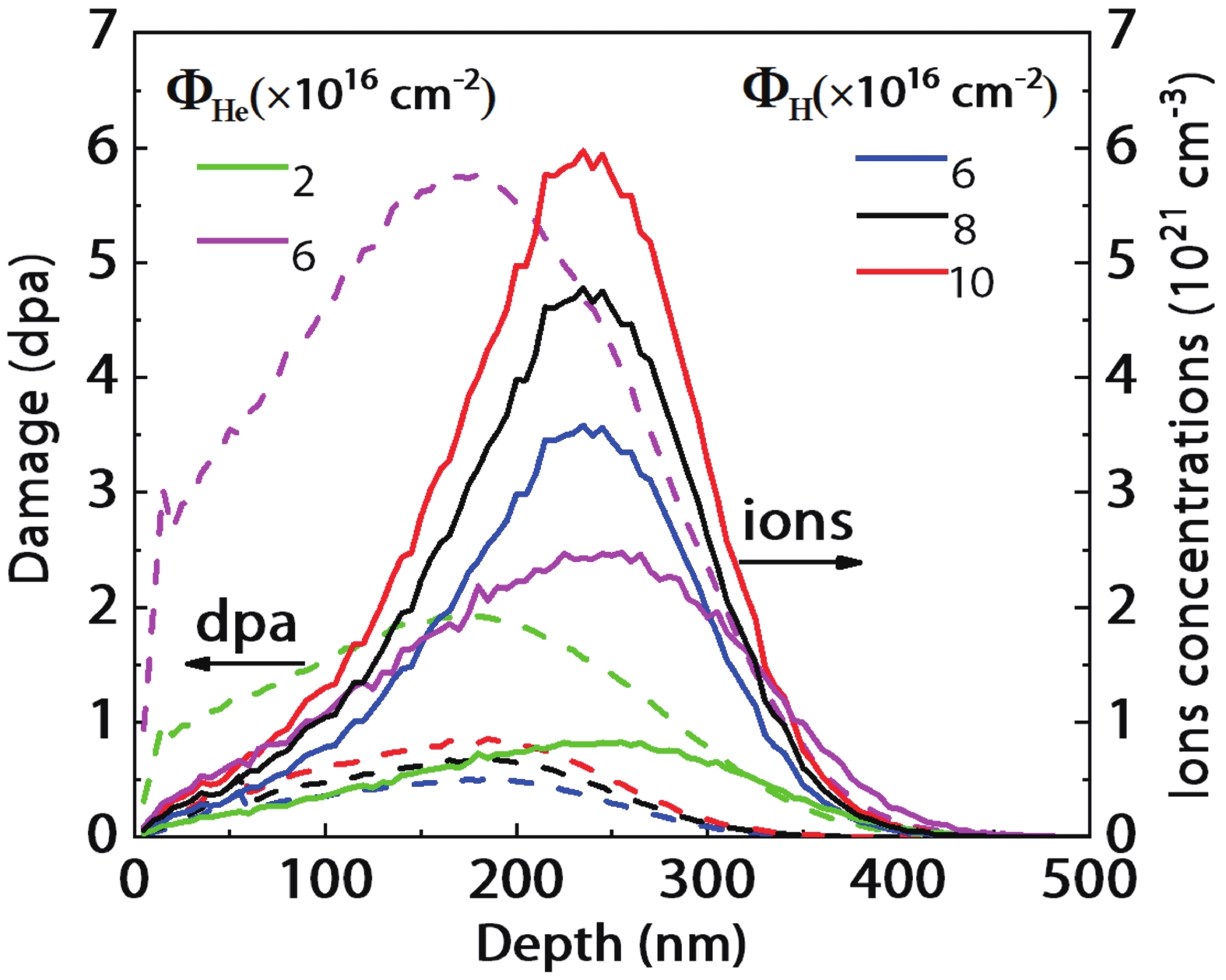
Fig. 1.
(Color online) Distribution of concentration and implantation damage with depth in GaAs crystal implanted with different fluences of H and He ions.
ARTICLES
Rui Huang1, , Zhiyong Wang2, Hui Li1, Qing Wang1 and Yecai Guo1
Corresponding author: Rui Huang, ruihuang@cwxu.edu.cn
Abstract: In this work, the surface morphology and internal defect evolution process of GaAs substrates implanted with light ions of different fluence combinations are studied. The influence of H and He ions implantation on the atomic mechanism of the blister phenomenon observed after annealing is investigated. Raman spectroscopy is used to measure the surface stress change of different samples before and after implantation and annealing. Optical microscopy and atomic force microscopy are used to characterize the morphology changes of the GaAs surface under different annealing conditions. The evolution of bubbles and defects in GaAs crystals is revealed by transmission electron microscopy. Through this study, it is hoped that ion implantation fluence, surface exfoliation efficiency and exfoliation cost can be optimized. At the same time, it also lays a foundation for the heterointegration of GaAs film on Si.
Keywords: surface morphology, internal defect evolution, surface stress, bubbles and defects
| [1] |
Bruel M. Silicon on insulator material technology. Electron Lett, 1995, 31, 1201 doi: 10.1049/el:19950805
|
| [2] |
Tong Q Y, Gösele U M. Wafer bonding and layer splitting for microsystems. Adv Mater, 1999, 11, 1409 doi: 10.1002/(SICI)1521-4095(199912)11:17<1409::AID-ADMA1409>3.0.CO;2-W
|
| [3] |
Singh R, Radu I, Scholz R, et al. Investigation of helium implantation induced blistering in InP. J Lumin, 2006, 121, 379 doi: 10.1016/j.jlumin.2006.08.073
|
| [4] |
Lin J, You T, Wang M, et al. Efficient ion-slicing of InP thin film for Si-based hetero-integration. Nanotechnology, 2018, 29, 504002 doi: 10.1088/1361-6528/aae281
|
| [5] |
Hebras X, Nguyen P, Bourdelle K K, et al. Comparison of platelet formation in hydrogen and helium-implanted silicon. Nucl Instruments Methods Phys Res Sect B, 2007, 262, 24 doi: 10.1016/j.nimb.2007.04.158
|
| [6] |
Cherkashin N, Daghbouj N, Darras F X, et al. Cracks and blisters formed close to a silicon wafer surface by He-H co-implantation at low energy. J Appl Phys, 2015, 118, 245301 doi: doi.org/10.1063/1.4938108
|
| [7] |
Personnic S, Bourdelle K K, Letertre F, et al. Impact of the transient formation of molecular hydrogen on the microcrack nucleation and evolution in H-implanted Si (001). J Appl Phys, 2008, 103, 023508 doi: 10.1063/1.2829807
|
| [8] |
Cherkashin N, Daghbouj N, Seine G, et al. Impact of He and H relative depth distributions on the result of sequential He+ and H+ ion implantation and annealing in silicon. J Appl Phys, 2018, 123, 161556 doi: 10.1063/1.5012505
|
| [9] |
Daghbouj N, Cherkashin N, Claverie A. A method to determine the pressure and densities of gas stored in blisters: Application to H and He sequential ion implantation in silicon. Microelectron Eng, 2018, 190, 54 doi: 10.1016/j.mee.2018.01.006
|
| [10] |
Daghbouj N, Cherkashin N, Darras F X, et al. Effect of the order of He+ and H+ ion co-implantation on damage generation and thermal evolution of complexes, platelets, and blisters in silicon. J Appl Phys, 2016, 119, 135308 doi: 10.1063/1.4945032
|
| [11] |
Nastasi M, Höchbauer T, Lee J K, et al. Nucleation and growth of platelets in hydrogen-ion-implanted silicon. Appl Phys Lett, 2005, 86, 154102 doi: 10.1063/1.1900309
|
| [12] |
Cherkashin N, Darras F X, Pochet P, et al. Modelling of point defect complex formation and its application to H+ ion implanted silicon. Acta Mater, 2015, 99, 187 doi: 10.1016/j.actamat.2015.07.078
|
| [13] |
Weldon M K. On the mechanism of the hydrogen-induced exfoliation of silicon. J Vac Sci Technol B, Microelectron Nanom Struct, 1997, 15, 1065 doi: 10.1116/1.589416
|
| [14] |
Reboh S, De Mattos A, Barbot J F, et al. Localized exfoliation versus delamination in H and He coimplanted (001) Si. J Appl Phys, 2009, 105, 093528 doi: 10.1063/1.3116738
|
| [15] |
Radu I, Szafraniak I, Scholz R, et al. GaAs on Si heterostructures obtained by He and/or H implantation and direct wafer bonding. J Appl Phys, 2003, 94, 7820 doi: 10.1063/1.1627459
|
| [16] |
Gawlik G, Jagielski J, Piatkowski B. GaAs on Si: Towards a low-temperature “smart-cut” technology. Vacuum, 2003, 70, 103 doi: 10.1016/S0042-207X(02)00627-9
|
| [17] |
Giguère A, Desrosiers N, Terreault B. Blistering effects of low energy hydrogen and helium ions implanted in GaAs(100) crystals. Nucl Instruments Methods Phys Res Sect B, 2006, 242, 620 doi: 10.1016/j.nimb.2005.08.187
|
| [18] |
Woo H J, Choi H W, Kim G D, et al. Blistering/exfoliation kinetics of GaAs by hydrogen and helium implantations. Surf Coatings Technol, 2009, 203, 2370 doi: 10.1016/j.surfcoat.2009.03.043
|
| [19] |
Sun J, Lin J, Jin T, et al. Efficient ion-slicing of 4-inch GaAs thin film for Si-based hetero-integration with ultra-smooth surface. Sci China Mater, 2022, 22, 211 doi: 10.1007/s40843-022-2135-y
|
| [20] |
Qian C, Terreault B. Blistering of silicon crystals by low keV hydrogen and helium ions. J Appl Phys, 2001, 90, 5152 doi: 10.1063/1.1413234
|
| [21] |
Barcz A, Kozubal M, Jakieła R, et al. Diffusion and impurity segregation in hydrogen-implanted silicon carbide. J Appl Phys, 2014, 115, 223710 doi: 10.1063/1.4882996
|
| [22] |
Li B S, Wang Z G, Zhang H P. Study of surface blistering in GaN by hydrogen implantation at elevated temperatures. Thin Solid Films, 2015, 590, 64 doi: 10.1016/j.tsf.2015.07.039
|
| [23] | |
| [24] |
Daghbouj N, Lin J, Sen H S, et al. Blister formation in He-H co-implanted InP: A comprehensive atomistic study. Appl Surf Sci, 2021, 552, 149426 doi: 10.1016/j.apsusc.2021.149426
|
| [25] |
Cevher Z, Folkes P A, Hier H S, et al. Optimization of the defects and the nonradiative lifetime of GaAs/AlGaAs double heterostructures. J Appl Phys, 2017, 123, 161512 doi: 10.1063/1.4986297
|
| [26] |
Jiménez J, Martín E, Prieto A C. Raman microprobe: a non-destructive tool for studying local misorientations in GaAs. Mater Lett, 1991, 12, 132 doi: 10.1016/0167-577X(91)90160-8
|
| [27] |
Gant T A, Shen H, Flemish J R, et al. Raman study of low growth temperature GaAs. Appl Phys Lett, 1992, 60, 12 doi: 10.1063/1.107347
|
| [28] |
Pizani P S, Lanciotti F, Jasinevicius R G, et al. Raman characterization of structural disorder and residual strains in micromachined GaAs. J Appl Phys, 2000, 87, 1280 doi: 10.1063/1.372009
|
| [29] |
Chandrasekaran N, Soga T, Jimbo T. GaAs film on Si substrate transplanted from GaAs/Ge structure by direct bonding. Appl Phys Lett, 2003, 82, 22 doi: 10.1063/1.1534915
|
| [30] |
Frabboni S, Corni F, Nobili C, et al. Nanovoid formation in helium-implanted single-crystal silicon studied by in situ techniques. Phys Rev B, 2004, 69, 165209 doi: 10.1103/PhysRevB.69.165209
|
| [31] |
Evans J H. Mechanisms of void coarsening in helium implanted silicon. Nucl Instruments Methods Phys Res Sect B, 2002, 196, 1 doi: 10.1016/S0168-583X(02)01246-6
|
| [32] |
Collino R R, Dick B B, Naab F, et al. Blister formation in ion-implanted GaAs: Role of diffusivity. Appl Phys Lett, 2009, 95, 111912 doi: 10.1063/1.3224199
|
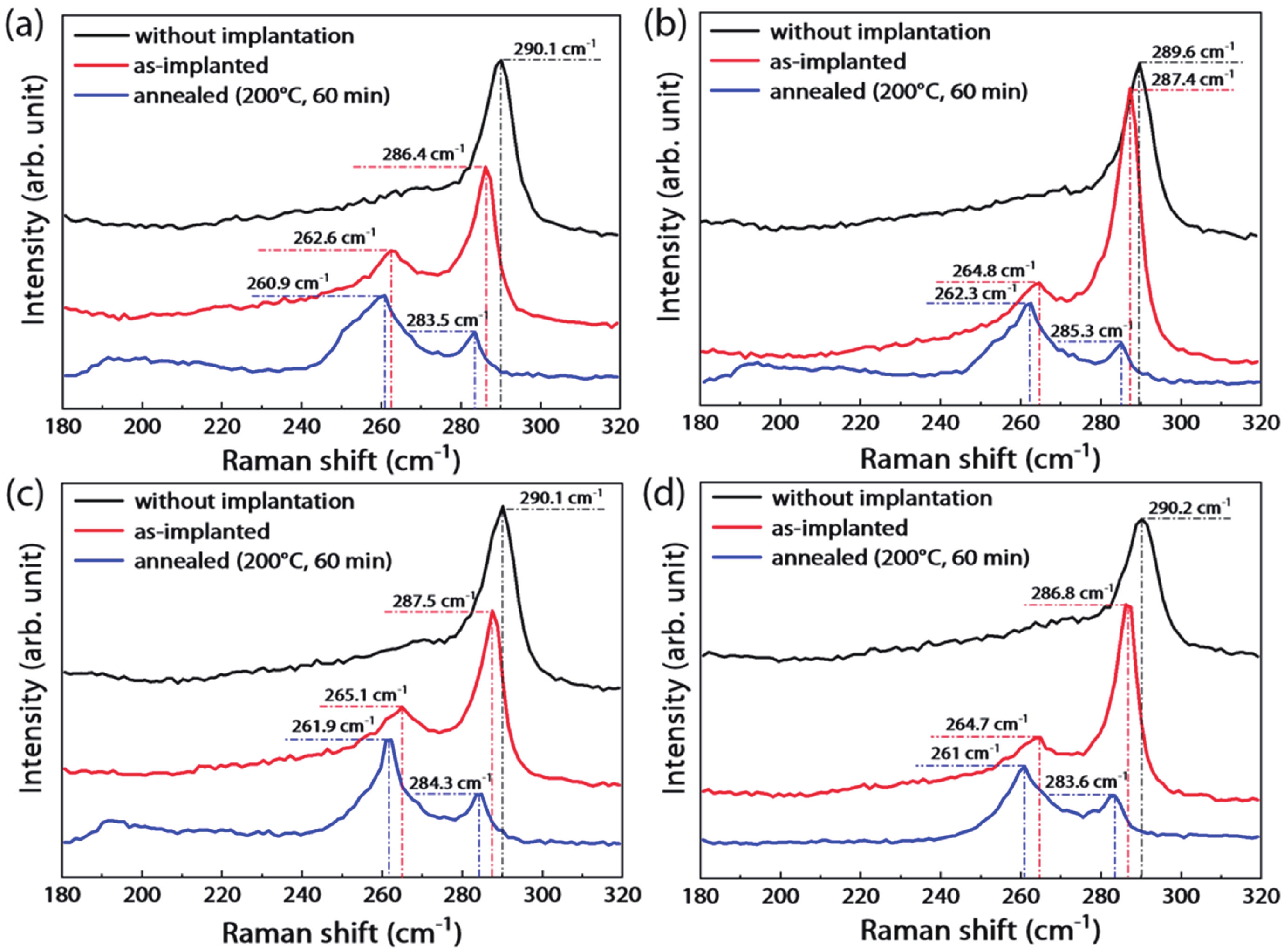
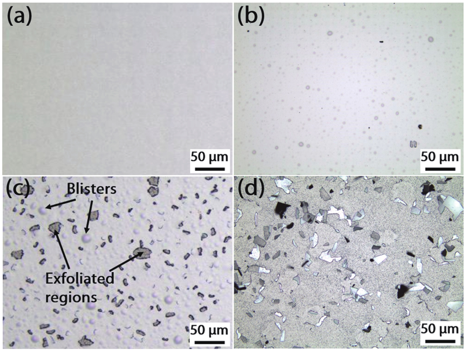
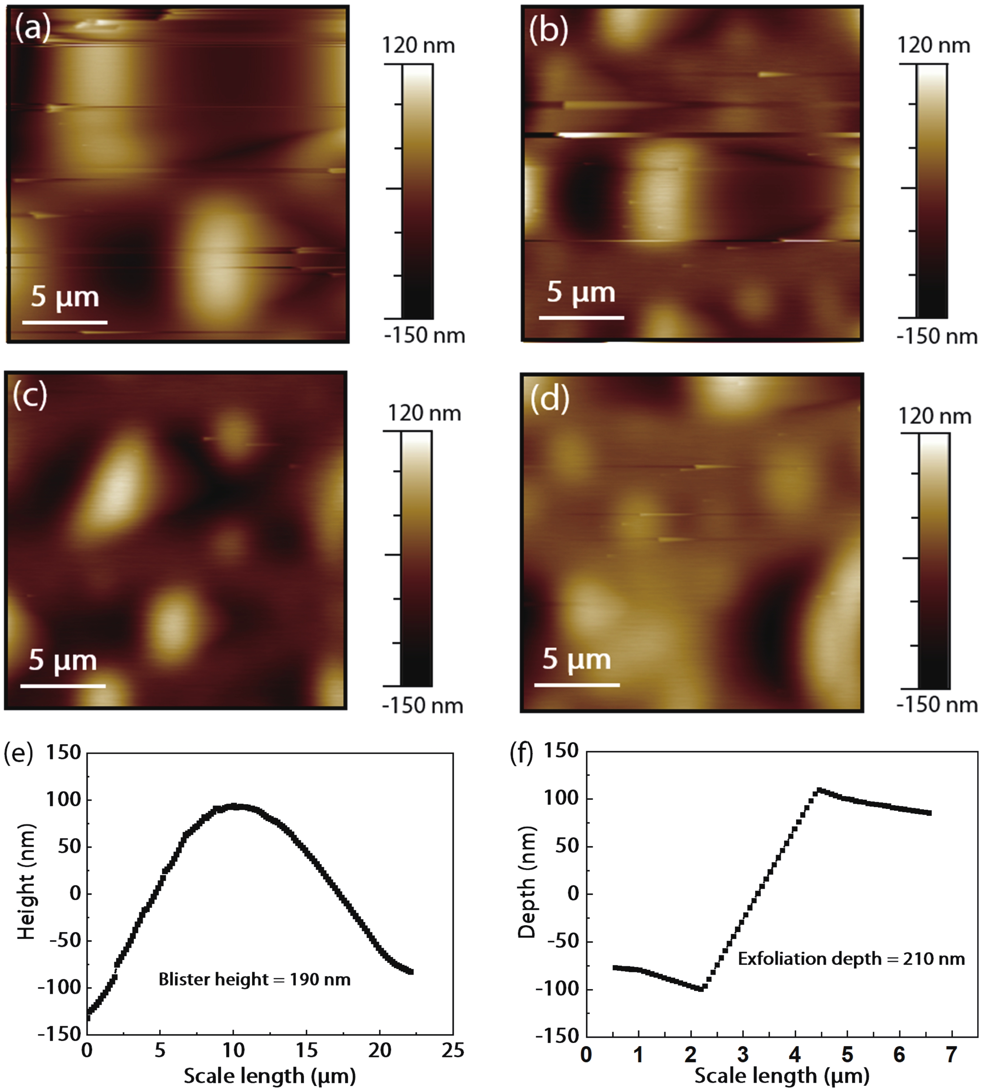
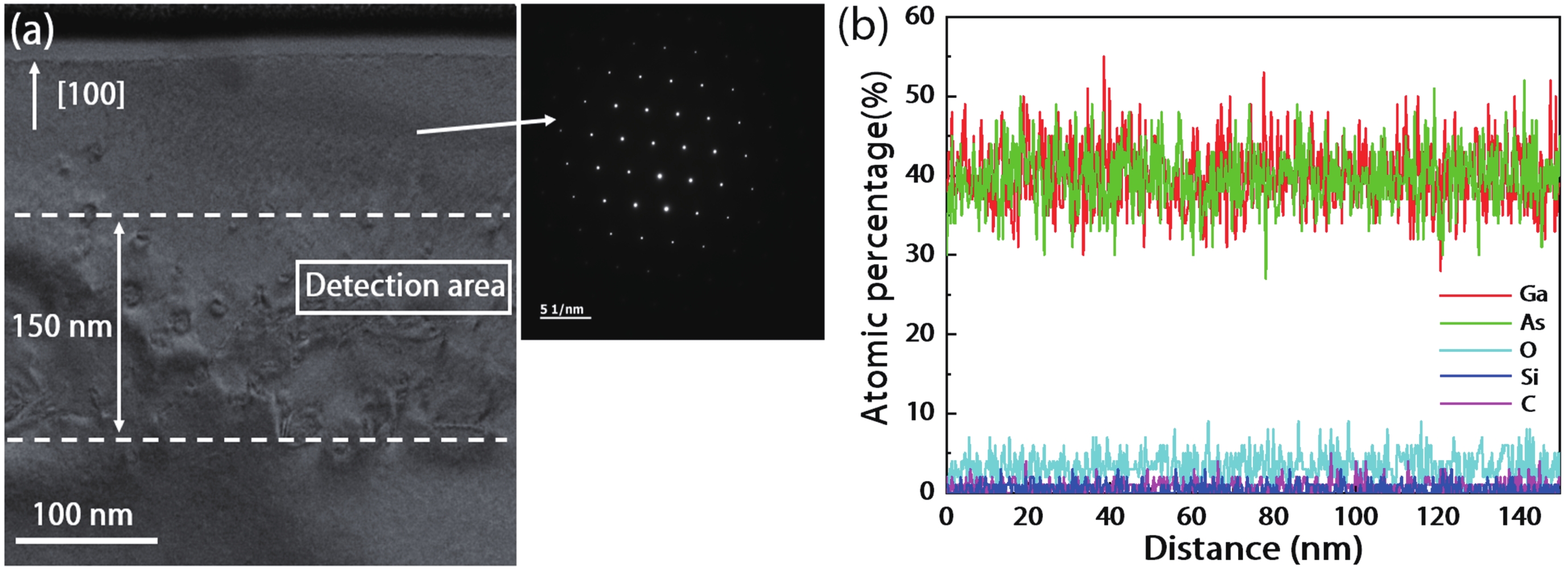
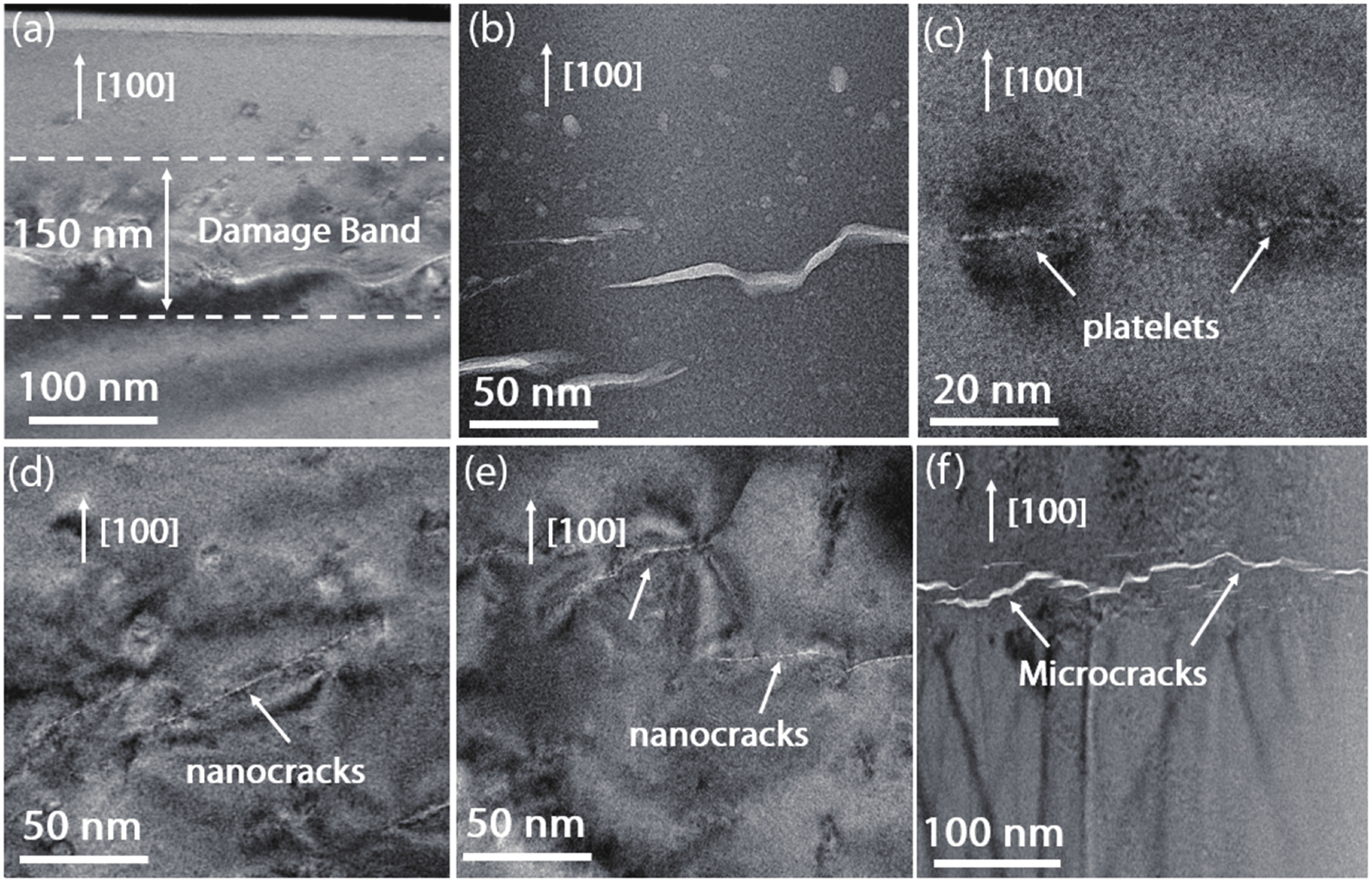
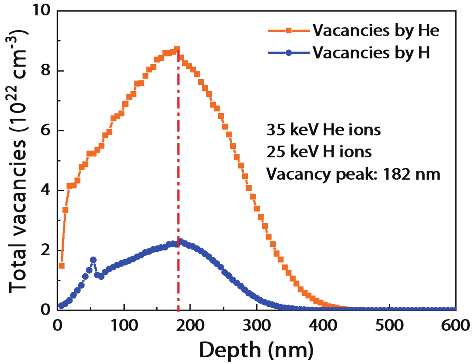
Table 1. Implantation parameters of four samples.
| Sample | Material | He+ fluence (1016 cm–2) | H+ fluence (1016 cm–2) | He+ energy (keV) | H+ energy (keV) |
| a | GaAs | 6 | — | 35 | — |
| b | GaAs | 2 | 6 | 35 | 25 |
| c | GaAs | — | 8 | — | 25 |
| d | GaAs | — | 10 | — | 25 |
 DownLoad: CSV
| [1] |
Bruel M. Silicon on insulator material technology. Electron Lett, 1995, 31, 1201 doi: 10.1049/el:19950805
|
| [2] |
Tong Q Y, Gösele U M. Wafer bonding and layer splitting for microsystems. Adv Mater, 1999, 11, 1409 doi: 10.1002/(SICI)1521-4095(199912)11:17<1409::AID-ADMA1409>3.0.CO;2-W
|
| [3] |
Singh R, Radu I, Scholz R, et al. Investigation of helium implantation induced blistering in InP. J Lumin, 2006, 121, 379 doi: 10.1016/j.jlumin.2006.08.073
|
| [4] |
Lin J, You T, Wang M, et al. Efficient ion-slicing of InP thin film for Si-based hetero-integration. Nanotechnology, 2018, 29, 504002 doi: 10.1088/1361-6528/aae281
|
| [5] |
Hebras X, Nguyen P, Bourdelle K K, et al. Comparison of platelet formation in hydrogen and helium-implanted silicon. Nucl Instruments Methods Phys Res Sect B, 2007, 262, 24 doi: 10.1016/j.nimb.2007.04.158
|
| [6] |
Cherkashin N, Daghbouj N, Darras F X, et al. Cracks and blisters formed close to a silicon wafer surface by He-H co-implantation at low energy. J Appl Phys, 2015, 118, 245301 doi: doi.org/10.1063/1.4938108
|
| [7] |
Personnic S, Bourdelle K K, Letertre F, et al. Impact of the transient formation of molecular hydrogen on the microcrack nucleation and evolution in H-implanted Si (001). J Appl Phys, 2008, 103, 023508 doi: 10.1063/1.2829807
|
| [8] |
Cherkashin N, Daghbouj N, Seine G, et al. Impact of He and H relative depth distributions on the result of sequential He+ and H+ ion implantation and annealing in silicon. J Appl Phys, 2018, 123, 161556 doi: 10.1063/1.5012505
|
| [9] |
Daghbouj N, Cherkashin N, Claverie A. A method to determine the pressure and densities of gas stored in blisters: Application to H and He sequential ion implantation in silicon. Microelectron Eng, 2018, 190, 54 doi: 10.1016/j.mee.2018.01.006
|
| [10] |
Daghbouj N, Cherkashin N, Darras F X, et al. Effect of the order of He+ and H+ ion co-implantation on damage generation and thermal evolution of complexes, platelets, and blisters in silicon. J Appl Phys, 2016, 119, 135308 doi: 10.1063/1.4945032
|
| [11] |
Nastasi M, Höchbauer T, Lee J K, et al. Nucleation and growth of platelets in hydrogen-ion-implanted silicon. Appl Phys Lett, 2005, 86, 154102 doi: 10.1063/1.1900309
|
| [12] |
Cherkashin N, Darras F X, Pochet P, et al. Modelling of point defect complex formation and its application to H+ ion implanted silicon. Acta Mater, 2015, 99, 187 doi: 10.1016/j.actamat.2015.07.078
|
| [13] |
Weldon M K. On the mechanism of the hydrogen-induced exfoliation of silicon. J Vac Sci Technol B, Microelectron Nanom Struct, 1997, 15, 1065 doi: 10.1116/1.589416
|
| [14] |
Reboh S, De Mattos A, Barbot J F, et al. Localized exfoliation versus delamination in H and He coimplanted (001) Si. J Appl Phys, 2009, 105, 093528 doi: 10.1063/1.3116738
|
| [15] |
Radu I, Szafraniak I, Scholz R, et al. GaAs on Si heterostructures obtained by He and/or H implantation and direct wafer bonding. J Appl Phys, 2003, 94, 7820 doi: 10.1063/1.1627459
|
| [16] |
Gawlik G, Jagielski J, Piatkowski B. GaAs on Si: Towards a low-temperature “smart-cut” technology. Vacuum, 2003, 70, 103 doi: 10.1016/S0042-207X(02)00627-9
|
| [17] |
Giguère A, Desrosiers N, Terreault B. Blistering effects of low energy hydrogen and helium ions implanted in GaAs(100) crystals. Nucl Instruments Methods Phys Res Sect B, 2006, 242, 620 doi: 10.1016/j.nimb.2005.08.187
|
| [18] |
Woo H J, Choi H W, Kim G D, et al. Blistering/exfoliation kinetics of GaAs by hydrogen and helium implantations. Surf Coatings Technol, 2009, 203, 2370 doi: 10.1016/j.surfcoat.2009.03.043
|
| [19] |
Sun J, Lin J, Jin T, et al. Efficient ion-slicing of 4-inch GaAs thin film for Si-based hetero-integration with ultra-smooth surface. Sci China Mater, 2022, 22, 211 doi: 10.1007/s40843-022-2135-y
|
| [20] |
Qian C, Terreault B. Blistering of silicon crystals by low keV hydrogen and helium ions. J Appl Phys, 2001, 90, 5152 doi: 10.1063/1.1413234
|
| [21] |
Barcz A, Kozubal M, Jakieła R, et al. Diffusion and impurity segregation in hydrogen-implanted silicon carbide. J Appl Phys, 2014, 115, 223710 doi: 10.1063/1.4882996
|
| [22] |
Li B S, Wang Z G, Zhang H P. Study of surface blistering in GaN by hydrogen implantation at elevated temperatures. Thin Solid Films, 2015, 590, 64 doi: 10.1016/j.tsf.2015.07.039
|
| [23] | |
| [24] |
Daghbouj N, Lin J, Sen H S, et al. Blister formation in He-H co-implanted InP: A comprehensive atomistic study. Appl Surf Sci, 2021, 552, 149426 doi: 10.1016/j.apsusc.2021.149426
|
| [25] |
Cevher Z, Folkes P A, Hier H S, et al. Optimization of the defects and the nonradiative lifetime of GaAs/AlGaAs double heterostructures. J Appl Phys, 2017, 123, 161512 doi: 10.1063/1.4986297
|
| [26] |
Jiménez J, Martín E, Prieto A C. Raman microprobe: a non-destructive tool for studying local misorientations in GaAs. Mater Lett, 1991, 12, 132 doi: 10.1016/0167-577X(91)90160-8
|
| [27] |
Gant T A, Shen H, Flemish J R, et al. Raman study of low growth temperature GaAs. Appl Phys Lett, 1992, 60, 12 doi: 10.1063/1.107347
|
| [28] |
Pizani P S, Lanciotti F, Jasinevicius R G, et al. Raman characterization of structural disorder and residual strains in micromachined GaAs. J Appl Phys, 2000, 87, 1280 doi: 10.1063/1.372009
|
| [29] |
Chandrasekaran N, Soga T, Jimbo T. GaAs film on Si substrate transplanted from GaAs/Ge structure by direct bonding. Appl Phys Lett, 2003, 82, 22 doi: 10.1063/1.1534915
|
| [30] |
Frabboni S, Corni F, Nobili C, et al. Nanovoid formation in helium-implanted single-crystal silicon studied by in situ techniques. Phys Rev B, 2004, 69, 165209 doi: 10.1103/PhysRevB.69.165209
|
| [31] |
Evans J H. Mechanisms of void coarsening in helium implanted silicon. Nucl Instruments Methods Phys Res Sect B, 2002, 196, 1 doi: 10.1016/S0168-583X(02)01246-6
|
| [32] |
Collino R R, Dick B B, Naab F, et al. Blister formation in ion-implanted GaAs: Role of diffusivity. Appl Phys Lett, 2009, 95, 111912 doi: 10.1063/1.3224199
|


Article views: 1840 Times PDF downloads: 79 Times Cited by: 0 Times
Received: 11 December 2022 Revised: 29 December 2022 Online: Accepted Manuscript: 27 February 2023Uncorrected proof: 28 February 2023Published: 10 May 2023
| Citation: |
Rui Huang, Zhiyong Wang, Hui Li, Qing Wang, Yecai Guo. Study of surface morphology in GaAs by hydrogen and helium implantation at elevated temperature[J]. Journal of Semiconductors, 2023, 44(5): 052102. doi: 10.1088/1674-4926/44/5/052102
****
R Huang, Z Y Wang, H Li, Q Wang, Y C Guo. Study of surface morphology in GaAs by hydrogen and helium implantation at elevated temperature[J]. J. Semicond, 2023, 44(5): 052102. doi: 10.1088/1674-4926/44/5/052102

|
 Rui Huang:received his Ph.D. degree at Beijing University of Technology. He is currently a lecturer in Wuxi University. His research mainly focuses on wafer bonding, smart-cut, semiconductor materials, additive manufacturing technologies and Silicon-based heterointegration
| [1] |
Bruel M. Silicon on insulator material technology. Electron Lett, 1995, 31, 1201 doi: 10.1049/el:19950805
|
| [2] |
Tong Q Y, Gösele U M. Wafer bonding and layer splitting for microsystems. Adv Mater, 1999, 11, 1409 doi: 10.1002/(SICI)1521-4095(199912)11:17<1409::AID-ADMA1409>3.0.CO;2-W
|
| [3] |
Singh R, Radu I, Scholz R, et al. Investigation of helium implantation induced blistering in InP. J Lumin, 2006, 121, 379 doi: 10.1016/j.jlumin.2006.08.073
|
| [4] |
Lin J, You T, Wang M, et al. Efficient ion-slicing of InP thin film for Si-based hetero-integration. Nanotechnology, 2018, 29, 504002 doi: 10.1088/1361-6528/aae281
|
| [5] |
Hebras X, Nguyen P, Bourdelle K K, et al. Comparison of platelet formation in hydrogen and helium-implanted silicon. Nucl Instruments Methods Phys Res Sect B, 2007, 262, 24 doi: 10.1016/j.nimb.2007.04.158
|
| [6] |
Cherkashin N, Daghbouj N, Darras F X, et al. Cracks and blisters formed close to a silicon wafer surface by He-H co-implantation at low energy. J Appl Phys, 2015, 118, 245301 doi: doi.org/10.1063/1.4938108
|
| [7] |
Personnic S, Bourdelle K K, Letertre F, et al. Impact of the transient formation of molecular hydrogen on the microcrack nucleation and evolution in H-implanted Si (001). J Appl Phys, 2008, 103, 023508 doi: 10.1063/1.2829807
|
| [8] |
Cherkashin N, Daghbouj N, Seine G, et al. Impact of He and H relative depth distributions on the result of sequential He+ and H+ ion implantation and annealing in silicon. J Appl Phys, 2018, 123, 161556 doi: 10.1063/1.5012505
|
| [9] |
Daghbouj N, Cherkashin N, Claverie A. A method to determine the pressure and densities of gas stored in blisters: Application to H and He sequential ion implantation in silicon. Microelectron Eng, 2018, 190, 54 doi: 10.1016/j.mee.2018.01.006
|
| [10] |
Daghbouj N, Cherkashin N, Darras F X, et al. Effect of the order of He+ and H+ ion co-implantation on damage generation and thermal evolution of complexes, platelets, and blisters in silicon. J Appl Phys, 2016, 119, 135308 doi: 10.1063/1.4945032
|
| [11] |
Nastasi M, Höchbauer T, Lee J K, et al. Nucleation and growth of platelets in hydrogen-ion-implanted silicon. Appl Phys Lett, 2005, 86, 154102 doi: 10.1063/1.1900309
|
| [12] |
Cherkashin N, Darras F X, Pochet P, et al. Modelling of point defect complex formation and its application to H+ ion implanted silicon. Acta Mater, 2015, 99, 187 doi: 10.1016/j.actamat.2015.07.078
|
| [13] |
Weldon M K. On the mechanism of the hydrogen-induced exfoliation of silicon. J Vac Sci Technol B, Microelectron Nanom Struct, 1997, 15, 1065 doi: 10.1116/1.589416
|
| [14] |
Reboh S, De Mattos A, Barbot J F, et al. Localized exfoliation versus delamination in H and He coimplanted (001) Si. J Appl Phys, 2009, 105, 093528 doi: 10.1063/1.3116738
|
| [15] |
Radu I, Szafraniak I, Scholz R, et al. GaAs on Si heterostructures obtained by He and/or H implantation and direct wafer bonding. J Appl Phys, 2003, 94, 7820 doi: 10.1063/1.1627459
|
| [16] |
Gawlik G, Jagielski J, Piatkowski B. GaAs on Si: Towards a low-temperature “smart-cut” technology. Vacuum, 2003, 70, 103 doi: 10.1016/S0042-207X(02)00627-9
|
| [17] |
Giguère A, Desrosiers N, Terreault B. Blistering effects of low energy hydrogen and helium ions implanted in GaAs(100) crystals. Nucl Instruments Methods Phys Res Sect B, 2006, 242, 620 doi: 10.1016/j.nimb.2005.08.187
|
| [18] |
Woo H J, Choi H W, Kim G D, et al. Blistering/exfoliation kinetics of GaAs by hydrogen and helium implantations. Surf Coatings Technol, 2009, 203, 2370 doi: 10.1016/j.surfcoat.2009.03.043
|
| [19] |
Sun J, Lin J, Jin T, et al. Efficient ion-slicing of 4-inch GaAs thin film for Si-based hetero-integration with ultra-smooth surface. Sci China Mater, 2022, 22, 211 doi: 10.1007/s40843-022-2135-y
|
| [20] |
Qian C, Terreault B. Blistering of silicon crystals by low keV hydrogen and helium ions. J Appl Phys, 2001, 90, 5152 doi: 10.1063/1.1413234
|
| [21] |
Barcz A, Kozubal M, Jakieła R, et al. Diffusion and impurity segregation in hydrogen-implanted silicon carbide. J Appl Phys, 2014, 115, 223710 doi: 10.1063/1.4882996
|
| [22] |
Li B S, Wang Z G, Zhang H P. Study of surface blistering in GaN by hydrogen implantation at elevated temperatures. Thin Solid Films, 2015, 590, 64 doi: 10.1016/j.tsf.2015.07.039
|
| [23] | |
| [24] |
Daghbouj N, Lin J, Sen H S, et al. Blister formation in He-H co-implanted InP: A comprehensive atomistic study. Appl Surf Sci, 2021, 552, 149426 doi: 10.1016/j.apsusc.2021.149426
|
| [25] |
Cevher Z, Folkes P A, Hier H S, et al. Optimization of the defects and the nonradiative lifetime of GaAs/AlGaAs double heterostructures. J Appl Phys, 2017, 123, 161512 doi: 10.1063/1.4986297
|
| [26] |
Jiménez J, Martín E, Prieto A C. Raman microprobe: a non-destructive tool for studying local misorientations in GaAs. Mater Lett, 1991, 12, 132 doi: 10.1016/0167-577X(91)90160-8
|
| [27] |
Gant T A, Shen H, Flemish J R, et al. Raman study of low growth temperature GaAs. Appl Phys Lett, 1992, 60, 12 doi: 10.1063/1.107347
|
| [28] |
Pizani P S, Lanciotti F, Jasinevicius R G, et al. Raman characterization of structural disorder and residual strains in micromachined GaAs. J Appl Phys, 2000, 87, 1280 doi: 10.1063/1.372009
|
| [29] |
Chandrasekaran N, Soga T, Jimbo T. GaAs film on Si substrate transplanted from GaAs/Ge structure by direct bonding. Appl Phys Lett, 2003, 82, 22 doi: 10.1063/1.1534915
|
| [30] |
Frabboni S, Corni F, Nobili C, et al. Nanovoid formation in helium-implanted single-crystal silicon studied by in situ techniques. Phys Rev B, 2004, 69, 165209 doi: 10.1103/PhysRevB.69.165209
|
| [31] |
Evans J H. Mechanisms of void coarsening in helium implanted silicon. Nucl Instruments Methods Phys Res Sect B, 2002, 196, 1 doi: 10.1016/S0168-583X(02)01246-6
|
| [32] |
Collino R R, Dick B B, Naab F, et al. Blister formation in ion-implanted GaAs: Role of diffusivity. Appl Phys Lett, 2009, 95, 111912 doi: 10.1063/1.3224199
|

 WeChat ID
Journal of Semiconductors © 2017 All Rights Reserved 京ICP备05085259号-2


