| Citation: |
Wenbo Tang, Xueli Han, Xiaodong Zhang, Botong Li, Yongjian Ma, Li Zhang, Tiwei Chen, Xin Zhou, Chunxu Bian, Yu Hu, Duanyang Chen, Hongji Qi, Zhongming Zeng, Baoshun Zhang. Homoepitaxial growth of (100) Si-doped β-Ga2O3 films via MOCVD[J]. Journal of Semiconductors, 2023, 44(6): 062801. doi: 10.1088/1674-4926/44/6/062801
****
W B Tang, X L Han, X D Zhang, B T Li, Y J Ma, L Zhang, T W Chen, X Zhou, C X Bian, Y Hu, D Y Chen, H J Qi, Z M Zeng, B S Zhang. Homoepitaxial growth of (100) Si-doped β-Ga2O3 films via MOCVD[J]. J. Semicond, 2023, 44(6): 062801. doi: 10.1088/1674-4926/44/6/062801
|
Homoepitaxial growth of (100) Si-doped β-Ga2O3 films via MOCVD
DOI: 10.1088/1674-4926/44/6/062801
More Information
-
Abstract
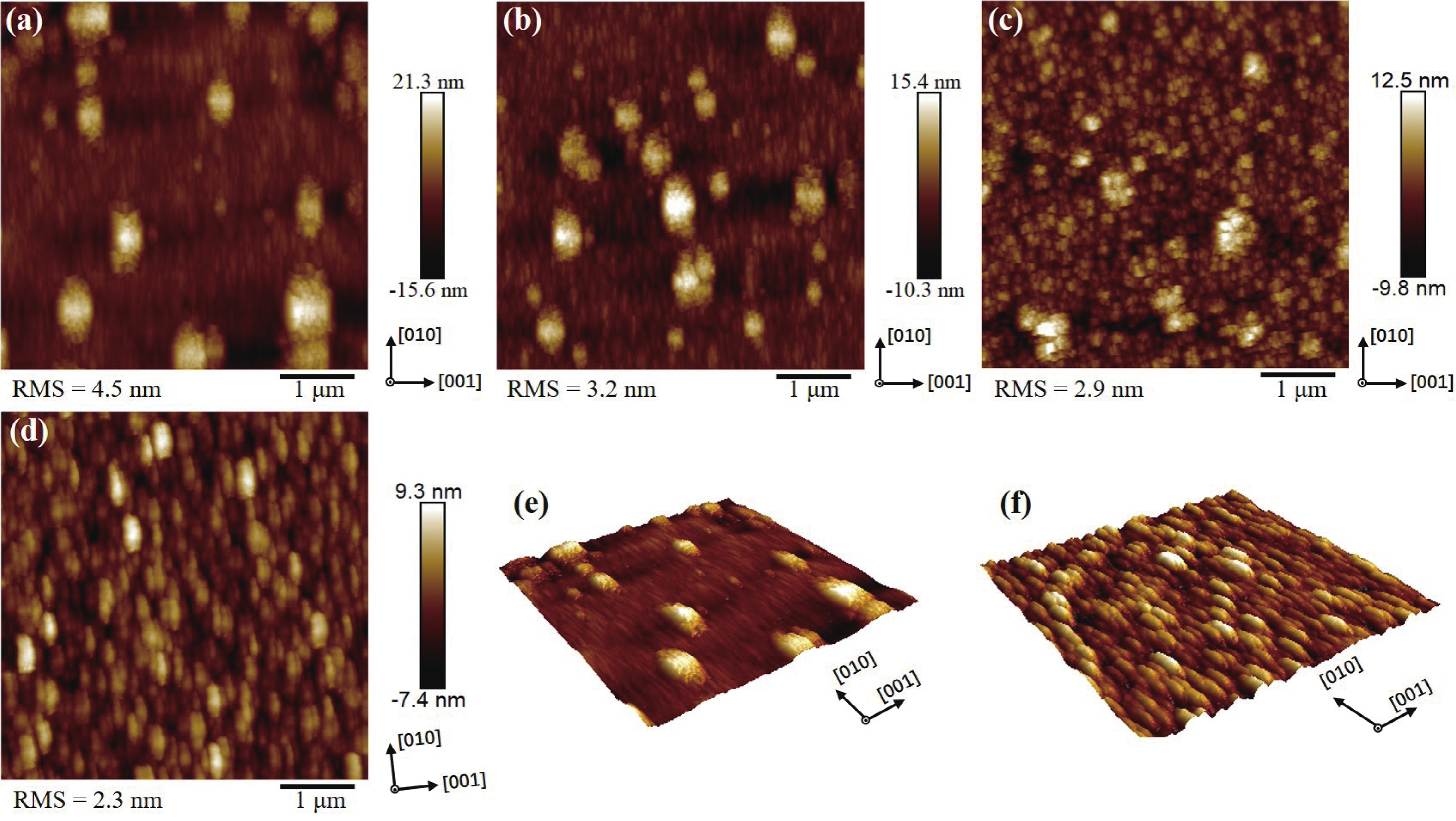
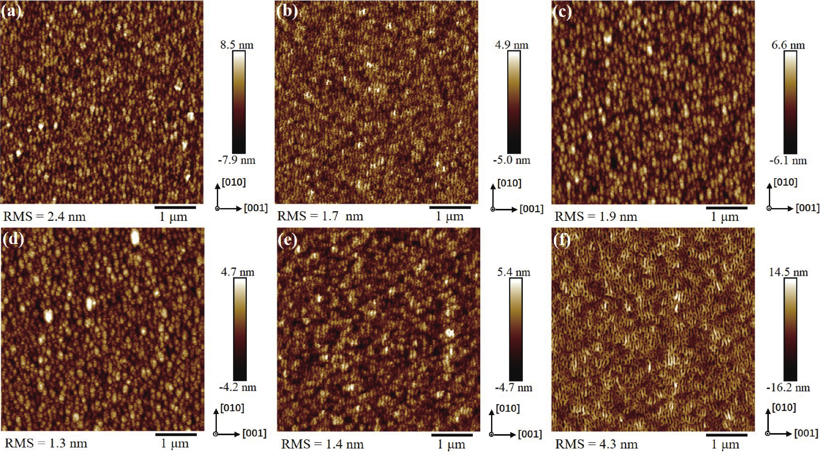
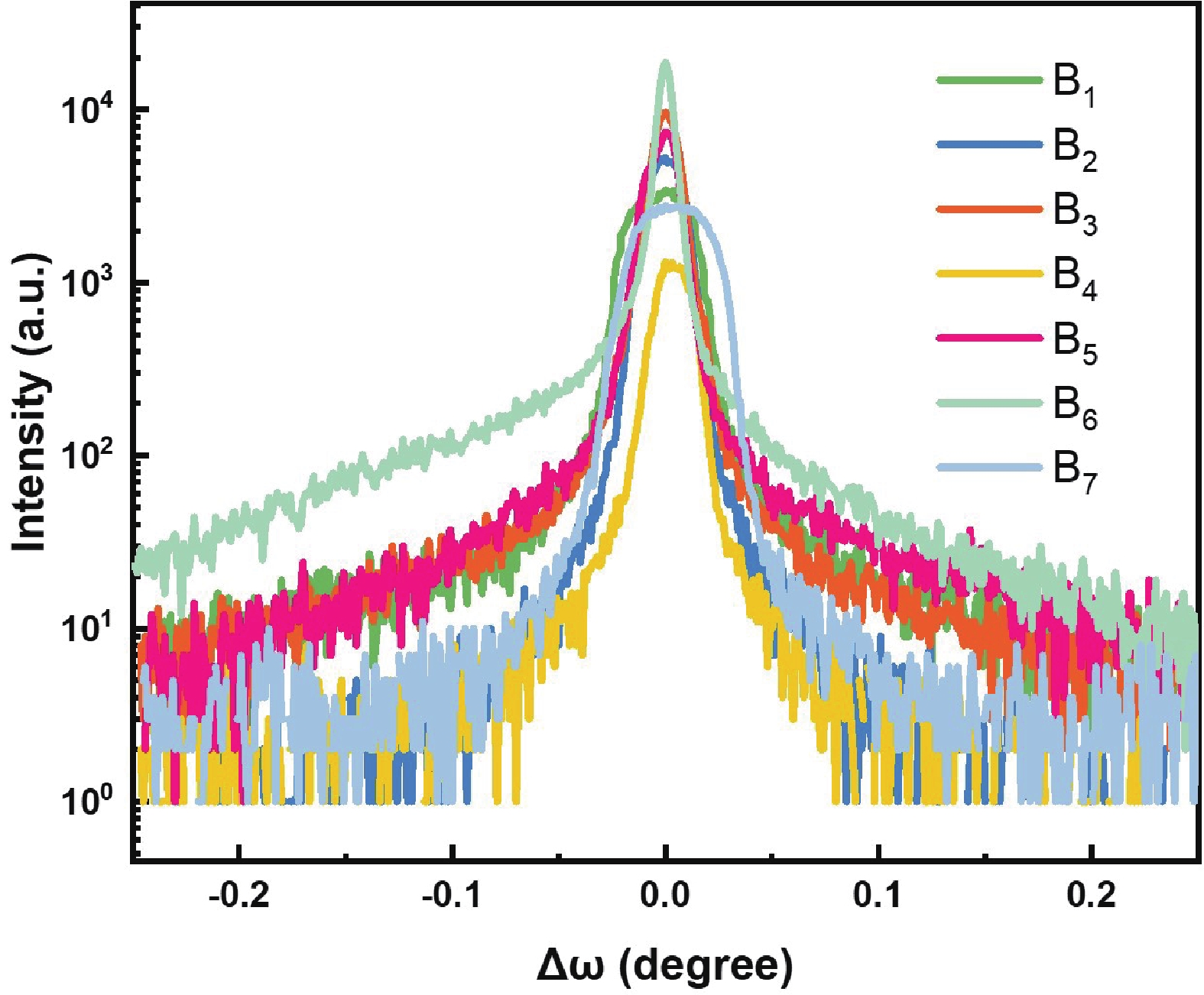
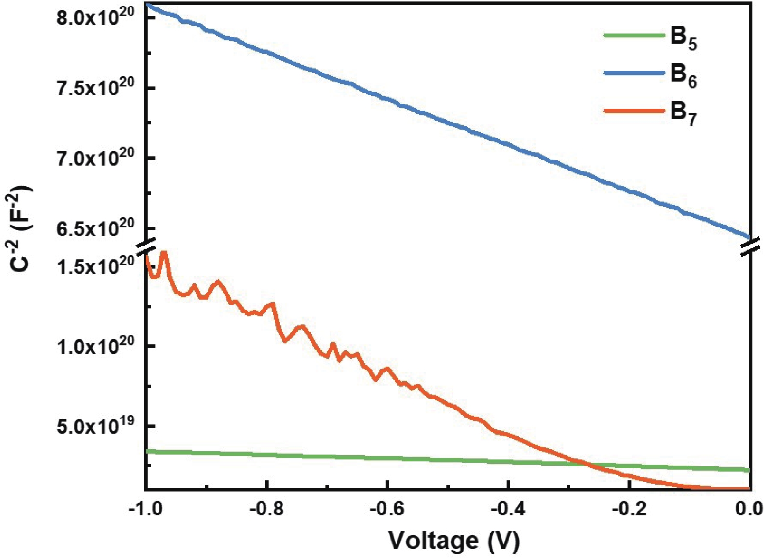
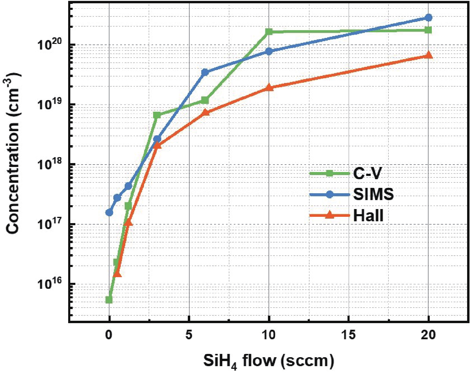
Homoepitaxial growth of Si-doped β-Ga2O3 films on semi-insulating (100) β-Ga2O3 substrates by metalorganic chemical vapor deposition (MOCVD) is studied in this work. By appropriately optimizing the growth conditions, an increasing diffusion length of Ga adatoms is realized, suppressing 3D island growth patterns prevalent in (100) β-Ga2O3 films and optimizing the surface morphology with [010] oriented stripe features. The slightly Si-doped β-Ga2O3 film shows smooth and flat surface morphology with a root-mean-square roughness of 1.3 nm. Rocking curves of the (400) diffraction peak also demonstrate the high crystal quality of the Si-doped films. According to the capacitance–voltage characteristics, the effective net doping concentrations of the films are 5.41 × 10¹⁵ – 1.74 × 1020 cm−3. Hall measurements demonstrate a high electron mobility value of 51 cm2/(V·s), corresponding to a carrier concentration of 7.19 × 1018 cm−3 and a high activation efficiency of up to 61.5%. Transmission line model (TLM) measurement shows excellent Ohmic contacts and a low specific contact resistance of 1.29 × 10⁻⁴ Ω·cm2 for the Si-doped film, which is comparable to the Si-implanted film with a concentration of 5.0 × 1019 cm−3, confirming the effective Si doing in the MOCVD epitaxy. -
References
[1] Wagner G, Baldini M, Gogova D, et al. Homoepitaxial growth of β-Ga2O3 layers by metal-organic vapor phase epitaxy. Phys Status Solidi A, 2014, 211, 27 doi: 10.1002/pssa.201330092[2] Higashiwaki M, Sasaki K, Kuramata A, et al. Development of gallium oxide power devices. Phys Status Solidi A, 2014, 211, 21 doi: 10.1002/pssa.201330197[3] Rafique S, Karim M R, Johnson J M, et al. LPCVD homoepitaxy of Si doped β-Ga2O3 thin films on (010) and (001) substrates. Appl Phys Lett, 2018, 112, 052104 doi: 10.1063/1.5017616[4] Tang W B, Zhang X D, He T, et al. Temperature-dependent electrical characteristics of β-Ga2O3 trench Schottky barrier diodes via self-reactive etching. J Phys D, 2021, 54, 425104 doi: 10.1088/1361-6463/ac1290[5] He Q M, Hao W B, Zhou X Z, et al. Over 1 GW/cm2 vertical Ga2O3 Schottky barrier diodes without edge termination. IEEE Electron Device Lett, 2022, 43, 264 doi: 10.1109/LED.2021.3133866[6] Lin C H, Yuda Y, Wong M H, et al. Vertical Ga2O3 Schottky barrier diodes with guard ring formed by nitrogen-ion implantation. IEEE Electron Device Lett, 2019, 40, 1487 doi: 10.1109/LED.2019.2927790[7] Wang Y B, Xu W H, Han G Q, et al. Channel properties of Ga2O3-on-SiC MOSFETs. IEEE Trans Electron Devices, 2021, 68, 1185 doi: 10.1109/TED.2021.3051135[8] Zeng K, Soman R, Bian Z L, et al. Vertical Ga2O3 MOSFET with magnesium diffused current blocking layer. IEEE Electron Device Lett, 2022, 43, 1527 doi: 10.1109/LED.2022.3196035[9] Huang H C, Ren Z J, Anhar Uddin Bhuiyan A F M, et al. β-Ga2O3 FinFETs with ultra-low hysteresis by plasma-free metal-assisted chemical etching. Appl Phys Lett, 2022, 121, 052102 doi: 10.1063/5.0096490[10] Hu Z Y, Nomoto K, Li W S, et al. 1.6 kV vertical Ga2O3 FinFETs with source-connected field plates and normally-off operation. 2019 31st International Symposium on Power Semiconductor Devices and ICs (ISPSD), 2019, 483 doi: 10.1109/ISPSD.2019.8757633[11] Fabris E, De Santi C, Caria A, et al. Trapping and detrapping mechanisms in β-Ga2O3 vertical FinFETs investigated by electro-optical measurements. IEEE Trans Electron Devices, 2020, 67, 3954 doi: 10.1109/TED.2020.3013242[12] Wong M H, Murakami H, Kumagai Y, et al. Aperture-limited conduction and its possible mechanism in ion-implanted current aperture vertical β-Ga2O3 MOSFETs. Appl Phys Lett, 2021, 118, 012102 doi: 10.1063/5.0031561[13] Wong M H, Murakami H, Kumagai Y, et al. Enhancement-mode β-Ga2O3 current aperture vertical MOSFETs with N-ion-implanted blocker. IEEE Electron Device Lett, 2020, 41, 296 doi: 10.1109/LED.2019.2962657[14] Sdoeung S, Sasaki K, Kawasaki K, et al. Line-shaped defects: Origin of leakage current in halide vapor-phase epitaxial (001) β-Ga2O3 Schottky barrier diodes. Appl Phys Lett, 2022, 120, 122107 doi: 10.1063/5.0088284[15] Sdoeung S, Sasaki K, Kawasaki K, et al. Probe-induced surface defects: Origin of leakage current in halide vapor-phase epitaxial (001) β-Ga2O3 Schottky barrier diodes. Appl Phys Lett, 2022, 120, 092101 doi: 10.1063/5.0085057[16] Huang H L, Chae C, Hwang J. Perspective on atomic scale investigation of point and extended defects in gallium oxide. J Appl Phys, 2022, 131, 190901 doi: 10.1063/5.0087053[17] Tadjer M J, Lyons J L, Nepal N, et al. Review—Theory and characterization of doping and defects in β-Ga2O3. ECS J Solid State Sci Technol, 2019, 8, Q3187 doi: 10.1149/2.0341907jss[18] Nishinaka H, Nagaoka T, Kajita Y, et al. Rapid homoepitaxial growth of (010) β-Ga2O3 thin films via mist chemical vapor deposition. Mater Sci Semicond Process, 2021, 128, 105732 doi: 10.1016/j.mssp.2021.105732[19] Goto K, Murakami H, Kuramata A, et al. Effect of substrate orientation on homoepitaxial growth of β-Ga2O3 by halide vapor phase epitaxy. Appl Phys Lett, 2022, 120, 102102 doi: 10.1063/5.0087609[20] Mazzolini P, Falkenstein A, Galazka Z, et al. Offcut-related step-flow and growth rate enhancement during (100) β-Ga2O3 homoepitaxy by metal-exchange catalyzed molecular beam epitaxy (MEXCAT-MBE). Appl Phys Lett, 2020, 117, 222105 doi: 10.1063/5.0031300[21] Mazzolini P, Bierwagen O. Towards smooth (010) β-Ga2O3 films homoepitaxially grown by plasma assisted molecular beam epitaxy: The impact of substrate offcut and metal-to-oxygen flux ratio. J Phys D, 2020, 53, 354003 doi: 10.1088/1361-6463/ab8eda[22] Zhang Y X, Feng Z X, Karim M R, et al. High-temperature low-pressure chemical vapor deposition of β-Ga2O3. J Vac Sci Technol A, 2020, 38, 050806 doi: 10.1116/6.0000360[23] Ranga P, Bhattacharyya A, Whittaker-Brooks L, et al. N-type doping of low-pressure chemical vapor deposition grown β-Ga2O3 thin films using solid-source germanium. J Vac Sci Technol A, 2021, 39, 030404 doi: 10.1116/6.0001004[24] Chou T S, Bin Anooz S, Grüneberg R, et al. Si doping mechanism in MOVPE-grown (100) β-Ga2O3 films. Appl Phys Lett, 2022, 121, 032103 doi: 10.1063/5.0096846[25] Ikenaga K, Tanaka N, Nishimura T, et al. Effect of high temperature homoepitaxial growth of β-Ga2O3 by hot-wall metalorganic vapor phase epitaxy. J Cryst Growth, 2022, 582, 126520 doi: 10.1016/j.jcrysgro.2022.126520[26] Tang W B, Ma Y J, Zhang X D, et al. High-quality (001) β-Ga2O3 homoepitaxial growth by metalorganic chemical vapor deposition enabled by in situ indium surfactant. Appl Phys Lett, 2022, 120, 212103 doi: 10.1063/5.0092754[27] Zhang W H, Zhang H Z, Zhang Z Z, et al. Heteroepitaxial β-Ga2O3 thick films on sapphire substrate by carbothermal reduction rapid growth method. Semicond Sci Technol, 2022, 37, 085014 doi: 10.1088/1361-6641/ac79c7[28] Mazzolini P, Falkenstein A, Wouters C, et al. Substrate-orientation dependence of β-Ga2O3 (100), (010), (001), and ( ${\bar{2}}01 $) homoepitaxy by indium-mediated metal-exchange catalyzed molecular beam epitaxy (MEXCAT-MBE). APL Mater, 2020, 8, 011107 doi: 10.1063/1.5135772[29] Mu S, Wang M G, Peelaers H, et al. First-principles surface energies for monoclinic Ga2O3 and Al2O3 and consequences for cracking of (AlxGa1−x)2O3. APL Mater, 2020, 8, 091105 doi: 10.1063/5.0019915[30] Anhar Uddin Bhuiyan A F M, Feng Z X, Johnson J M, et al. MOCVD epitaxy of ultrawide bandgap β-(AlxGa1–x)2O3 with high-Al composition on (100) β-Ga2O3 substrates. Cryst Growth Des, 2020, 20, 6722 doi: 10.1021/acs.cgd.0c00864[31] Bin Anooz S, Grüneberg R, Wouters C, et al. Step flow growth of β-Ga2O3 thin films on vicinal (100) β-Ga2O3 substrates grown by MOVPE. Appl Phys Lett, 2020, 116, 182106 doi: 10.1063/5.0005403[32] Schewski R, Lion K, Fiedler A, et al. Step-flow growth in homoepitaxy of β-Ga2O3 (100)—The influence of the miscut direction and faceting. APL Mater, 2018, 7, 022515 doi: 10.1063/1.5054943[33] Wang C L, Zhou H, Zhang J C, et al. Hysteresis-free and μs-switching of D/E-modes Ga2O3 hetero-junction FETs with the BV2/Ron, sp of 0.74/0.28 GW/cm2. Appl Phys Lett, 2022, 120, 112101 doi: 10.1063/5.0084804[34] Wang C L, Zhang J C, Xu S R, et al. Progress in state-of-the-art technologies of Ga2O3 devices. J Phys D:Appl Phys, 2021, 54, 243001 doi: 10.1088/1361-6463/abe158[35] Sasaki K, Higashiwaki M, Kuramata A, et al. Si-ion implantation doping in β-Ga2O3 and its application to fabrication of low-resistance ohmic contacts. Appl Phys Express, 2013, 6, 086502 doi: 10.7567/APEX.6.086502[36] Oshima T, Arai N, Suzuki N, et al. Surface morphology of homoepitaxial β-Ga2O3 thin films grown by molecular beam epitaxy. Thin Solid Films, 2008, 516, 5768 doi: 10.1016/j.tsf.2007.10.045[37] Meng L Y, Bhuiyan A F M A U, Feng Z X, et al. Metalorganic chemical vapor deposition of (100) β-Ga2O3 on on-axis Ga2O3 substrates. J Vac Sci Technol A, 2022, 40, 062706 doi: 10.1116/6.0002179[38] Ngo T S, Le D D, Lee J, et al. Investigation of defect structure in homoepitaxial ( ${\bar{2}}01 $) β-Ga2O3 layers prepared by plasma-assisted molecular beam epitaxy. J Alloys Compd, 2020, 834, 155027 doi: 10.1016/j.jallcom.2020.155027[39] Bhuiyan A F M A U, Feng Z X, Johnson J M, et al. MOCVD growth of β-phase (AlxGa1−x)2O3 on ( ${\bar{2}}01 $) β-Ga2O3 substrates. Appl Phys Lett, 2020, 117, 142107 doi: 10.1063/5.0025478[40] Ma P P, Zheng J, Zhang Y B, et al. Investigation on n-type ( ${\bar{2}}01 $) β-Ga2O3 ohmic contact via Si ion implantation. Tsinghua Sci Technol, 2023, 28, 150 doi: 10.26599/TST.2021.9010039[41] Nikolskaya A, Okulich E, Korolev D, et al. Ion implantation in β-Ga2O3: Physics and technology. J Vac Sci Technol A, 2021, 39, 030802 doi: 10.1116/6.0000928[42] Lee M H, Chou T S, Bin Anooz S, et al. Exploiting the nanostructural anisotropy of β-Ga2O3 to demonstrate giant improvement in titanium/gold ohmic contacts. ACS Nano, 2022, 16, 11988 doi: 10.1021/acsnano.2c01957[43] Sharma R, Law M E, Ren F, et al. Diffusion of dopants and impurities in β-Ga2O3. J Vac Sci Technol A, 2021, 39, 060801 doi: 10.1116/6.0001307[44] Zhang Y N, Zhang J C, Feng Z Q, et al. Impact of implanted edge termination on vertical β-Ga2O3 Schottky barrier diodes under OFF-state stressing. IEEE Trans Electron Devices, 2020, 67, 3948 doi: 10.1109/TED.2020.3002327[45] Ranga P, Bhattacharyya A, Chmielewski A, et al. Growth and characterization of metalorganic vapor-phase epitaxy-grown β-(AlxGa1–x)2O3/β-Ga2O3 heterostructure channels. Appl Phys Express, 2021, 14, 025501 doi: 10.35848/1882-0786/abd675 -
Proportional views


 DownLoad:


 Wenbo Tang:is a PhD student at University of Science and Technology of China and Suzhou Institute of Nano-Tech and Nano-Bionics of Chinese Academy of Sciences under the supervision of Prof. Baoshun Zhang. His research focuses on the homoepitaxy and power electronics of β-Ga2O3
 Hongji Qi:received his BS degree from Zhengzhou University in 2000 and his PhD degree from Shanghai Institute of Optics and Fine Mechanics, Chinese Academy of Sciences in 2005. After that, he stayed at the institute as an assistant researcher and became a full researcher in 2011. His research interests include nonlinear crystal materials, novel semiconductor materials and scintillation crystal materials
 Baoshun Zhang:received his BS degree from Changchun University of Science and Technology in 1994 and PhD degree from the Institute of Semiconductors, Chinese Academy of Sciences in 2003. Then he joined in Hong Kong University of Science and Technology. Currently, he is a researcher at Suzhou Institute of Nano-Tech and Nano-Bionics, Chinese Academy of Sciences, and his research interests include semiconductor material growth and device technology research


