J. Semicond. > 2023, Volume 44 > Issue 7 > 071801

REVIEWS

Anisotropic optical and electric properties of β-gallium oxide

Yonghui Zhang and Fei Xing

+ Author Affiliations

 Corresponding author: Yonghui Zhang, yhzhang@sdut.edu.cn; Fei Xing, xingfei@sdut.edu.cn

DOI: 10.1088/1674-4926/44/7/071801

PDF

Turn off MathJax

Abstract: The anisotropic properties and applications of β-gallium oxide (β-Ga2O3) are comprehensively reviewed. All the anisotropic properties are essentially resulted from the anisotropic crystal structure. The process flow of how to exfoliate nanoflakes from bulk material is introduced. Anisotropic optical properties, including optical bandgap, Raman and photoluminescence characters are comprehensively reviewed. Three measurement configurations of angle-resolved polarized Raman spectra (ARPRS) are reviewed, with Raman intensity formulas calculated with Raman tensor elements. The method to obtain the Raman tensor elements of phonon modes through experimental fitting is also introduced. In addition, the anisotropy in electron mobility and affinity are discussed. The applications, especially polarization photodetectors, based on β-Ga2O3 were summarized comprehensively. Three kinds of polarization detection mechanisms based on material dichroism, 1D morphology and metal-grids are discussed in-depth. This review paper provides a framework for anisotropic optical and electric properties of β-Ga2O3, as well as the applications based on these characters, and is expected to lead to a wider discussion on this topic.

Key words: gallium oxideanisotropicdichroismpolarizationmonoclinic


[1]
Liang H L, Han Z Y, Mei Z X. Recent progress of deep ultraviolet photodetectors using amorphous gallium oxide thin films. Phys Status Solidi A, 2021, 218, 2000339 doi: 10.1002/pssa.202000339
[2]
Kaur D, Kumar M. A strategic review on gallium oxide based deep-ultraviolet photodetectors: Recent progress and future prospects. Adv Optical Mater, 2021, 9, 2002160 doi: 10.1002/adom.202002160
[3]
Atilgan A, Yildiz A, Harmanci U, et al. β-Ga2O3 nanoflakes/p-Si heterojunction self-powered photodiodes. Mater Today Commun, 2020, 24, 101105 doi: 10.1016/j.mtcomm.2020.101105
[4]
Jian L Y, Lee H Y, Lee C T. Ga2O3-based p-i-n solar blind deep ultraviolet photodetectors. J Mater Sci: Mater Electron, 2019, 30, 8445 doi: 10.1007/s10854-019-01163-w
[5]
Zhao B, Wang F, Chen H Y, et al. An ultrahigh responsivity (9.7 mA W–1) self-powered solar-blind photodetector based on individual ZnO-Ga2O3 heterostructures. Adv Funct Mater, 2017, 27, 1700264 doi: 10.1002/adfm.201700264
[6]
Chen M Z, Ma J G, Li P, et al. Zero-biased deep ultraviolet photodetectors based on graphene/cleaved (100) Ga2O3 heterojunction. Opt Express, 2019, 27, 8717 doi: 10.1364/OE.27.008717
[7]
Cui S J, Mei Z X, Zhang Y H, et al. Room-temperature fabricated amorphous Ga2O3 high-response-speed solar-blind photodetector on rigid and flexible substrates. Adv Opt Mater, 2017, 5, 1700454 doi: 10.1002/adom.201700454
[8]
Zhao B, Wang F, Chen H, et al. Solar-blind avalanche photodetector based on single ZnO–Ga2O3 core–shell microwire. Nano Lett, 2015, 15, 3988 doi: 10.1021/acs.nanolett.5b00906
[9]
Han Z Y, Liang H L, Huo W X, et al. Boosted UV photodetection performance in chemically etched amorphous Ga2O3 thin-film transistors. Adv Optical Mater, 2020, 8, 1901833 doi: 10.1002/adom.201901833
[10]
Qin Y, Long S, He Q, et al. Amorphous gallium oxide-based gate-tunable high-performance thin film phototransistor for solar-blind imaging. Adv Electron Mater, 2019, 5, 1900389 doi: 10.1002/aelm.201900389
[11]
Wang Y, Cui W, Yu J, et al. One-step growth of Amorphous/Crystalline Ga2O3 phase junctions for high-performance solar-blind photodetection. ACS Appl Mater Interfaces, 2019, 11, 45922 doi: 10.1021/acsami.9b17409
[12]
Chi Z Y, Asher J J, Jennings M R, et al. Ga2O3 and related ultra-wide bandgap power semiconductor oxides: New energy electronics solutions for CO2 emission mitigation. Materials, 2022, 15, 1164 doi: 10.3390/ma15031164
[13]
Hu Z, Zhou H, Feng Q, et al. Field-plated lateral β-Ga2O3 Schottky barrier diode with high reverse blocking voltage of more than 3 kV and high DC power figure-of-merit of 500 MW/cm2. IEEE Electron Device Lett, 2018, 39, 1564 doi: 10.1109/LED.2018.2868444
[14]
Sharma S, Zeng K, Saha S, et al. Field-plated lateral Ga2O3 MOSFETs with polymer passivation and 8.03 kV breakdown voltage. IEEE Electron Device Lett, 2020, 41, 836 doi: 10.1109/LED.2020.2991146
[15]
Sui Y X, Liang H L, Chen Q S, et al. Room-temperature ozone sensing capability of IGZO-decorated amorphous Ga2O3 films. ACS Appl Mater Interfaces, 2020, 12, 8929 doi: 10.1021/acsami.9b22400
[16]
Liang H, Cui S, Su R, et al. Flexible X-ray detectors based on amorphous Ga2O3 thin films. ACS Photonics, 2018, 6, 351 doi: 10.1021/acsphotonics.8b00769
[17]
Geller S. Crystal structure of β-Ga2O3. J Chem Phys, 1960, 33, 676 doi: 10.1063/1.1731237
[18]
Lorenz M R, Woods J F, Gambino R J. Some electrical properties of the semiconductor β-Ga2O3. J Phys Chem Solids, 1967, 28, 403 doi: 10.1016/0022-3697(67)90305-8
[19]
Li L, Han W, Pi L, et al. Emerging in-plane anisotropic two-dimensional materials. InfoMat, 2019, 1, 54 doi: 10.1002/inf2.12005
[20]
Binet L, Gourier D. Origin of the blue luminescence of β-Ga2O3. J Phys Chem Solids, 1998, 59, 1241 doi: 10.1016/S0022-3697(98)00047-X
[21]
Binet L, Gourier D, Minot C. Relation between electron band structure and magnetic bistability of conduction electrons in β-Ga2O3. J Solid State Chem, 1994, 113, 420 doi: 10.1006/jssc.1994.1390
[22]
Hwang W S, Verma A, Peelaers H, et al. High-voltage field effect transistors with wide-bandgap β-Ga2O3 nanomembranes. Appl Phys Lett, 2014, 104, 203111 doi: 10.1063/1.4879800
[23]
Åhman J, Svensson G, Albertsson J. A reinvestigation of β-gallium oxide. Acta Crystallogr C, 1996, 52, 1336 doi: 10.1107/S0108270195016404
[24]
Oh S, Mastro M A, Tadjer M J, et al. Solar-blind metal-semiconductor-metal photodetectors based on an exfoliated β-Ga2O3 Micro-flake. ECS J Solid State Sci Technol, 2017, 6, Q79 doi: 10.1149/2.0231708jss
[25]
Liu X L, Zhang X, Lin M L, et al. Different angle-resolved polarization configurations of Raman spectroscopy: A case on the basal and edge plane of two-dimensional materials. Chin Phys B, 2017, 26, 067802 doi: 10.1088/1674-1056/26/6/067802
[26]
Li Z, Liu Y, Zhang A, et al. Quasi-two-dimensional β-Ga2O3 field effect transistors with large drain current density and low contact resistance via controlled formation of interfacial oxygen vacancies. Nano Res, 2019, 12, 143 doi: 10.1007/s12274-018-2193-7
[27]
Chen J X, Li X X, Huang W, et al. High-energy X-ray radiation effects on the exfoliated quasi-two-dimensional β-Ga2O3 nanoflake field-effect transistors. Nanotechnology, 2020, 31, 345206 doi: 10.1088/1361-6528/ab925d
[28]
Bae J, Kim H W, Kang I H, et al. High breakdown voltage quasi-two-dimensional β-Ga2O3 field-effect transistors with a boron nitride field plate. Appl Phys Lett, 2018, 112, 122102 doi: 10.1063/1.5018238
[29]
Kwon Y, Lee G, Oh S, et al. Tuning the thickness of exfoliated quasi-two-dimensional β-Ga2O3 flakes by plasma etching. Appl Phys Lett, 2017, 110, 131901 doi: 10.1063/1.4979028
[30]
Kim J, Mastro M A, Tadjer M J, et al. Quasi-two-dimensional h-BN/β-Ga2O3 heterostructure metal-insulator-semiconductor field-effect transistor. ACS Appl Mater Interfaces, 2017, 9, 21322 doi: 10.1021/acsami.7b04374
[31]
Ueda N, Hosono H, Waseda R, et al. Anisotropy of electrical and optical properties in β-Ga2O3 single crystals. Appl Phys Lett, 1997, 71, 933 doi: 10.1063/1.119693
[32]
Varley J B, Weber J R, Janotti A, et al. Oxygen vacancies and donor impurities in β-Ga2O3. Appl Phys Lett, 2010, 97, 142106 doi: 10.1063/1.3499306
[33]
Ricci F, Boschi F, Baraldi A, et al. Theoretical and experimental investigation of optical absorption anisotropy in β-Ga2O3. J Phys:Conden Matter, 2016, 28, 224005 doi: 10.1088/0953-8984/28/22/224005
[34]
Yamaguchi K. First principles study on electronic structure of β-Ga2O3. Solid State Commun, 2004, 131, 739 doi: 10.1016/j.ssc.2004.07.030
[35]
Chen X, Mu W, Xu Y, et al. Highly narrow-band polarization-sensitive solar-blind photodetectors based on β-Ga2O3 single crystals. ACS Appl Mater Interfaces, 2019, 11, 7131 doi: 10.1021/acsami.8b19524
[36]
Mu W, Chen X, He G, et al. Anisotropy and in-plane polarization of low-symmetrical β-Ga2O3 single crystal in the deep ultraviolet band. Appl Surf Sci, 2020, 527, 146648 doi: 10.1016/j.apsusc.2020.146648
[37]
Zhang N J, Kislyakov I M, Xia C T, et al. Anisotropic luminescence and third-order electric susceptibility of Mg-doped gallium oxide under the half-bandgap edge. Opt Express, 2021, 29, 18587 doi: 10.1364/OE.427021
[38]
Bilbao Crystallographic Server, https://www.cryst.ehu.es/ (accessed August 15, 2022)
[39]
Kranert C, Sturm C, Schmidt-Grund R, et al. Raman tensor elements of β-Ga2O3. Sci Rep, 2016, 6, 1 doi: 10.1038/s41598-016-0001-8
[40]
Jones R C. A new calculus for the treatment of optical SystemsI description and discussion of the calculus. J Opt Soc Am, 1941, 31, 488 doi: 10.1364/JOSA.31.000488
[41]
Frodason Y K, Johansen K M, Vines L, et al. Self-trapped hole and impurity-related broad luminescence in β-Ga2O3. J Appl Phys, 2020, 127, 075701 doi: 10.1063/1.5140742
[42]
Marcinkevičius S, Speck J S. Ultrafast dynamics of hole self-localization in β-Ga2O3. Appl Phys Lett, 2020, 116, 132101 doi: 10.1063/5.0003682
[43]
Yang J C, Ren F, Tadjer M, et al. 2300V reverse breakdown voltage Ga2O3Schottky rectifiers. ECS J Solid State Sci Technol, 2018, 7, Q92 doi: 10.1149/2.0241805jss
[44]
Wong M H, Sasaki K, Kuramata A, et al. Field-plated Ga2O3 MOSFETs with a breakdown voltage of over 750 V. IEEE Electron Device Lett, 2016, 37, 212 doi: 10.1109/LED.2015.2512279
[45]
Ghosh K, Singisetti U. Ab initio calculation of electron-phonon coupling in monoclinic β-Ga2O3 crystal. Appl Phys Lett, 2016, 109, 072102 doi: 10.1063/1.4961308
[46]
Ghosh K, Singisetti U. Low-field and high-field transport in β-Ga2O3. In: Gallium Oxide. Elsevier, 2019
[47]
Li Z, Wang Q, Feng C, et al. Simulation study of performance degradation in β-Ga2O3 (001) vertical Schottky barrier diodes based on anisotropic mobility modeling. ECS J Solid State Sci Technol, 2021, 10, 055005 doi: 10.1149/2162-8777/abed98
[48]
Higashiwaki M, Konishi K, Sasaki K, et al. Temperature-dependent capacitance–voltage and current–voltage characteristics of Pt/Ga2O3 (001) Schottky barrier diodes fabricated on n–Ga2O3 drift layers grown by halide vapor phase epitaxy. Appl Phys Lett, 2016, 108, 133503 doi: 10.1063/1.4945267
[49]
Vavoulas A, Sandalidis H G, Chatzidiamantis N D, et al. A survey on ultraviolet C-band (UV-C) communications. IEEE Commun Surv Tutorials, 2019, 21, 2111 doi: 10.1109/COMST.2019.2898946
[50]
Chen Q, Zhang Y H, Zheng T, et al. Polarization detection in deep-ultraviolet light with monoclinic gallium oxide nanobelts. Nanoscale Adv, 2020, 2, 2705 doi: 10.1039/D0NA00364F
[51]
Wang J F, Gudiksen M S, Duan X F, et al. Highly polarized photoluminescence and photodetection from single indium phosphide nanowires. Science, 2001, 293, 1455 doi: 10.1126/science.1062340
[52]
Soria E, Gomez-Rodriguez P, Tromas C, et al. Self-assembled, 10 nm-tailored, near infrared plasmonic metasurface acting as broadband omnidirectional polarizing mirror. Adv Opt Mater, 2020, 8, 2000321 doi: 10.1002/adom.202000321
[53]
Oh S, Lee J H, Lee H J, et al. Polarized ultraviolet emitters with Al wire-grid polarizers fabricated by solvent-assisted nanotransfer process. Nanotechnology, 2019, 31, 045304 doi: 10.1088/1361-6528/ab4c16
[54]
Sun D, Feng B, Yang B, et al. Design and fabrication of an InGaAs focal plane array integrated with linear-array polarization grating. Opt Lett, 2020, 45, 1559 doi: 10.1364/OL.376110
[55]
Freitas Carvalho F, Augusto de Moraes Cruz C, Costa Marques G, et al. Angular light, polarization and stokes parameters information in a hybrid image sensor with division of focal plane. Sensors, 2020, 20, 3391 doi: 10.3390/s20123391
[56]
Zhang Y H, Wang Z X, Xing F. Enhancement of polarization response in UVA and UVC wavelength with integrated sub-wavelength metal-grids. Microelectron Eng, 2021, 242/243, 111555 doi: 10.1016/j.mee.2021.111555
[57]
Vasyltsiv V I, Rym Y I, Zakharko Y M. Optical absorption and photoconductivity at the band edge of β-Ga2–xInxO3. Phys Stat Sol B, 1996, 195, 653 doi: 10.1002/pssb.2221950232
[58]
Yang Y, Liu S C, Wang X, et al. Polarization-sensitive ultraviolet photodetection of anisotropic 2D GeS2. Adv Funct Mater, 2019, 29, 1900411 doi: 10.1002/adfm.201900411
[59]
Li L, Gao W, Chen H Y, et al. Strong anisotropy and piezo-phototronic effect in SnO2 microwires. Adv Electron Mater, 2020, 6, 1901441 doi: 10.1002/aelm.201901441
[60]
Tabares G, Hierro A, Vinter B, et al. Polarization-sensitive Schottky photodiodes based on a-plane ZnO/ZnMgO multiple quantum-wells. Appl Phys Lett, 2011, 99, 071108 doi: 10.1063/1.3624924
[61]
Fan Z, Chang P C, Lu J G, et al. Photoluminescence and polarized photodetection of single ZnO nanowires. Appl Phys Lett, 2004, 85, 6128 doi: 10.1063/1.1841453
[62]
Rivera C, Pau J L, Muñoz E, et al. Polarization-sensitive ultraviolet photodetectors based on M-plane GaN grown on LiAlO2 substrates. Appl Phys Lett, 2006, 88, 213507 doi: 10.1063/1.2206128
[63]
Han S, Jin W, Zhang D H, et al. Photoconduction studies on GaN nanowire transistors under UV and polarized UV illumination. Chem Phys Lett, 2004, 389, 176 doi: 10.1016/j.cplett.2004.03.083
[64]
Yang Y, Liu S C, Yang W, et al. Air-stable in-plane anisotropic GeSe2 for highly polarization-sensitive photodetection in short wave region. J Am Chem Soc, 2018, 140, 4150 doi: 10.1021/jacs.8b01234
[65]
Yan Y, Xiong W, Li S, et al. Direct wide bandgap 2D GeSe2 monolayer toward anisotropic UV photodetection. Adv Optl Mater, 2019, 7, 1900622 doi: 10.1002/adom.201900622
[66]
Zhou Y, Luo J, Zhao Y, et al. Flexible linearly polarized photodetectors based on all-inorganic perovskite CsPbI3 nanowires. Adv Opt Mater, 2018, 6, 1800679 doi: 10.1002/adom.201800679
[67]
Singh A, Li X, Protasenko V, et al. Polarization-sensitive nanowire photodetectors based on solution-synthesized CdSe quantum-wire solids. Nano Lett, 2007, 7, 2999 doi: 10.1021/nl0713023
[68]
Wang X, Wu K, Blei M, et al. Highly polarized photoelectrical response in vdW ZrS3 nanoribbons. Adv Electron Mater, 2019, 5, 1900419 doi: 10.1002/aelm.201900419
[69]
Liu D, Hong J, Wang X, et al. Diverse atomically sharp interfaces and linear dichroism of 1T'ReS2-ReSe2 lateral p–n heterojunctions. Adv Funct Mater, 2018, 28, 1804696 doi: 10.1002/adfm.201804696
[70]
Gao L, Zeng K, Guo J, et al. Passivated single-crystalline CH3NH3PbI3 nanowire photodetector with high detectivity and polarization sensitivity. Nano Lett, 2016, 16(12), 7446 doi: 10.1021/acs.nanolett.6b03119
[71]
Liu F, Zheng S, He X, et al. Highly sensitive detection of polarized light using anisotropic 2D ReS2. Adv Funct Mater, 2016, 26, 1169 doi: 10.1002/adfm.201504546
[72]
Liu S, Xiao W, Zhong M, et al. Highly polarization sensitive photodetectors based on quasi-1D titanium trisulfide (TiS3). Nanotechnology, 2018, 29, 184002 doi: 10.1088/1361-6528/aaafa2
[73]
Li L, Gong P, Sheng D, et al. Highly in-plane anisotropic 2D GeAs2 for polarization-sensitive photodetection. Adv Mater, 2018, 30, 1804541 doi: 10.1002/adma.201804541
[74]
Yang S, Hu C, Wu M, et al. In-plane optical anisotropy and linear dichroism in low-symmetry layered TlSe. ACS Nano, 2018, 12, 8798 doi: 10.1021/acsnano.8b05162
[75]
Hong T, Chamlagain B, Wang T J, et al. Anisotropic photocurrent response at black phosphorus-MoS2 p–n heterojunctions. Nanoscale, 2015, 7, 18537 doi: 10.1039/C5NR03400K
[76]
Yuan H, Liu X, Afshinmanesh F, et al. Polarization-sensitive broadband photodetector using a black phosphorus vertical p–n junction. Nat Nanotechnol, 2015, 10, 707 doi: 10.1038/nnano.2015.112
[77]
Mitdank R, Dusari S, Bülow C, et al. Temperature-dependent electrical characterization of exfoliated β-Ga2O3 micro flakes. Phys Status Solidi A, 2014, 211, 543 doi: 10.1002/pssa.201330671
[78]
Kim J, Oh S, Mastro M A, et al. Exfoliated β-Ga2O3 nano-belt field-effect transistors for air-stable high power and high temperature electronics. Phys Chem Chem Phys, 2016, 18, 15760 doi: 10.1039/C6CP01987K
[79]
Guo Z, Verma A, Wu X, et al. Anisotropic thermal conductivity in single crystal β-gallium oxide. Appl Phys Lett, 2015, 106, 111909 doi: 10.1063/1.4916078
[80]
Handwerg M, Mitdank R, Galazka Z, et al. Temperature-dependent thermal conductivity in Mg-doped and undoped β-Ga2O3 bulk-crystals. Semicond Sci Technol, 2015, 30, 024006 doi: 10.1088/0268-1242/30/2/024006
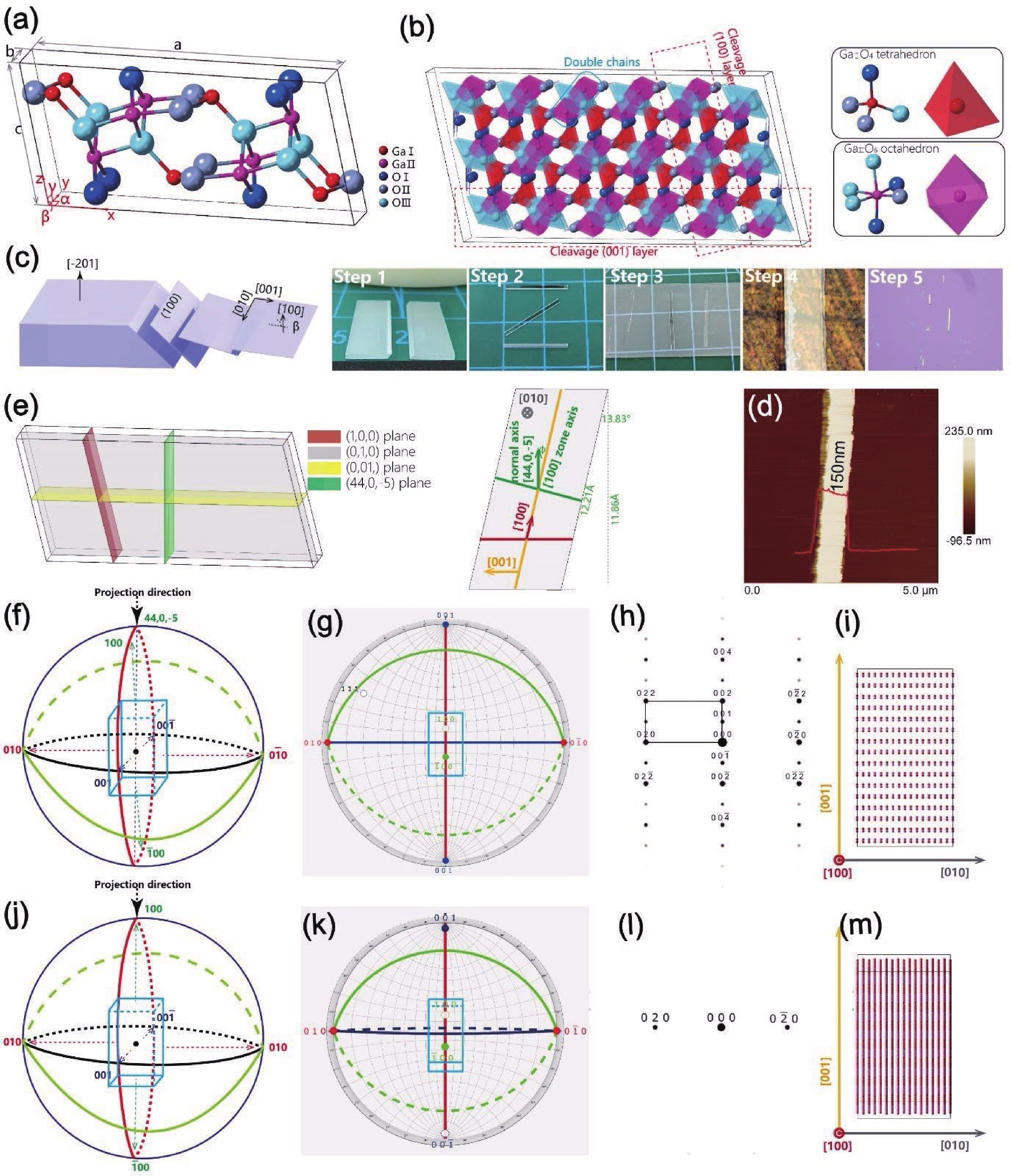
Fig. 1.  (Color online) Anisotropic cystal structure of β-Ga2O3. (a) Unit cell of β-Ga2O3. (b) 2 × 2 cells with GaO4 tetrahedral and GaO6 octahedral chains. (c) Process flow of mechanical exfoliation of β-Ga2O3 nanobelts. (d) AFM result of one typical β-Ga2O3 nanobelt. (e) Lattice frame of β-Ga2O3. (f) Stereographic projection, (g) projection plane, (h) electron diffraction pattern and (i) projection view of β-Ga2O3 along [44, 0, –5] direction. (j) Stereographic projection, (k) projection plane, (l) electron diffraction pattern and (m) projection view of β-Ga2O3 along [100] direction.

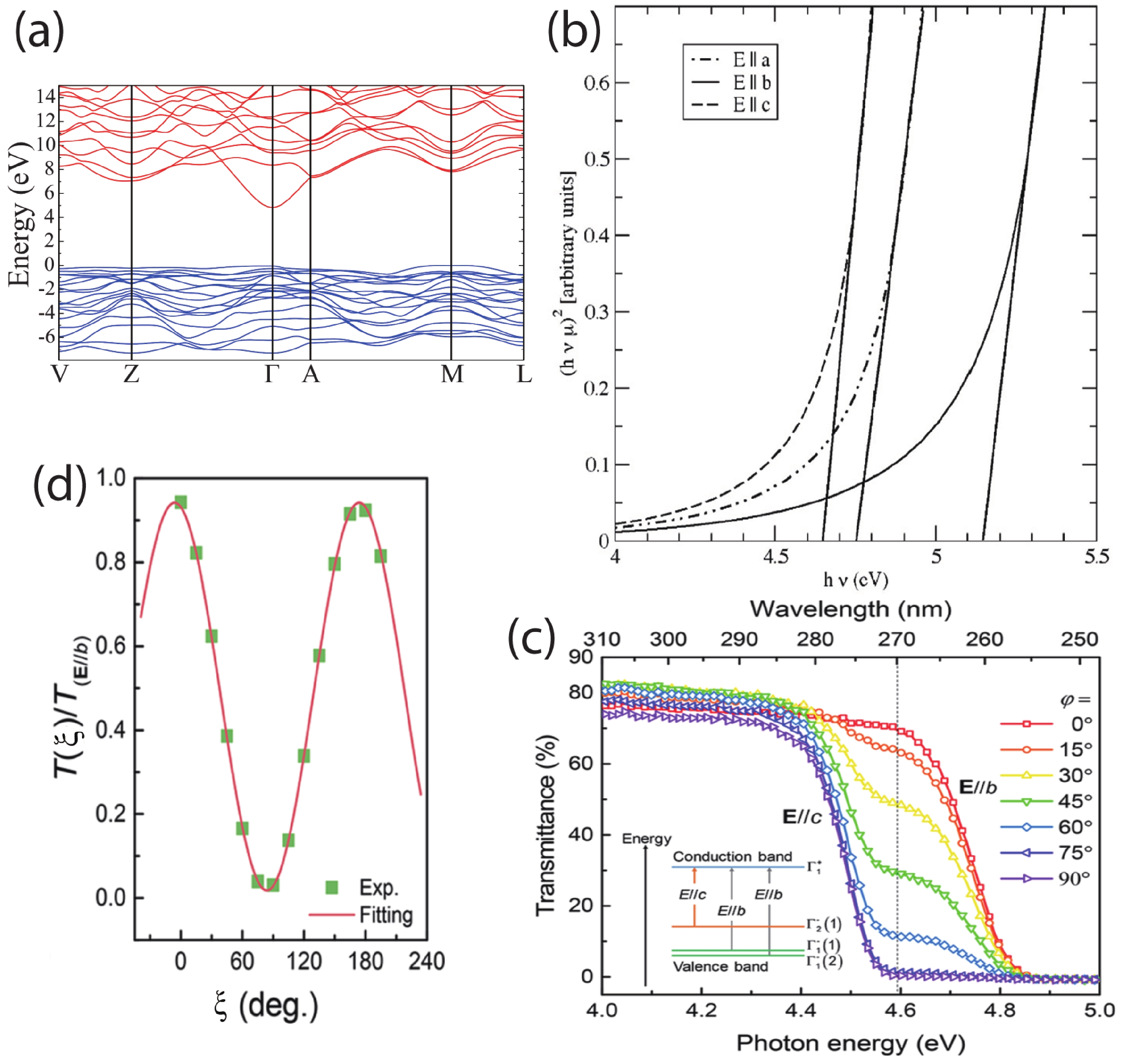
Fig. 2.  (Color online) Anisotropic optical bandgap of β-Ga2O3. (a) Band structure for β-Ga2O3 calculated using the primitive unit cell of base-centered monoclinic[32]. Copyright 2010 by AIP publishing. (b) Tauc plot of the absorption coefficient, showing the polarization-dependent onsets[33]. Copyright 2016 by IOP publishing. (c) Polarized transmittance spectra of a β-Ga2O3 (100) single crystal and (d) transmittance magnitude with respect to E//b as a function of in-plane polarization angle[35]. Copyright 2019 by American Chemical Society.

Fig. 3.  (Color online) Schematic diagrams of three typical polarization configurations for angle-resolved polarized Raman spectroscopy[25]. Copyright 2017 by IOP publishing. (a) The schematic diagram of type 1 configuration. Polar plots of the Raman intensity when the analyzer is set along (b) vertical and (c) horizontal directions. (d) The schematic diagram of type 2 configuration. Polar plots of the Raman intensity when the analyzer is set along (e) vertical and (f) horizontal directions. The schematic diagram of type 3 configuration. Polar plots of the Raman intensity when the analyzer is (h) vertical and (i) horizontal to the incident laser direction.

Fig. 4.  (Color online) ARPRS results and Raman tensor elements from literature[39]. (a) Raman scattering intensities (circles), model fits (solid lines) and modelled intensities from ab-intio-calculated tensor elements (dashed lines) of the phonon modes with Ag-symmetry of β-Ga2O3 for parallel (black) and cross polarization (red) in dependence on the direction of the (scattered) polarization ϕ. (b) Raman tensor elements of Ag modes. (c) Raman scattering intensities and (d) Raman tensor elements of Bg modes. Copyright 2016 by Nature Publishing Group.

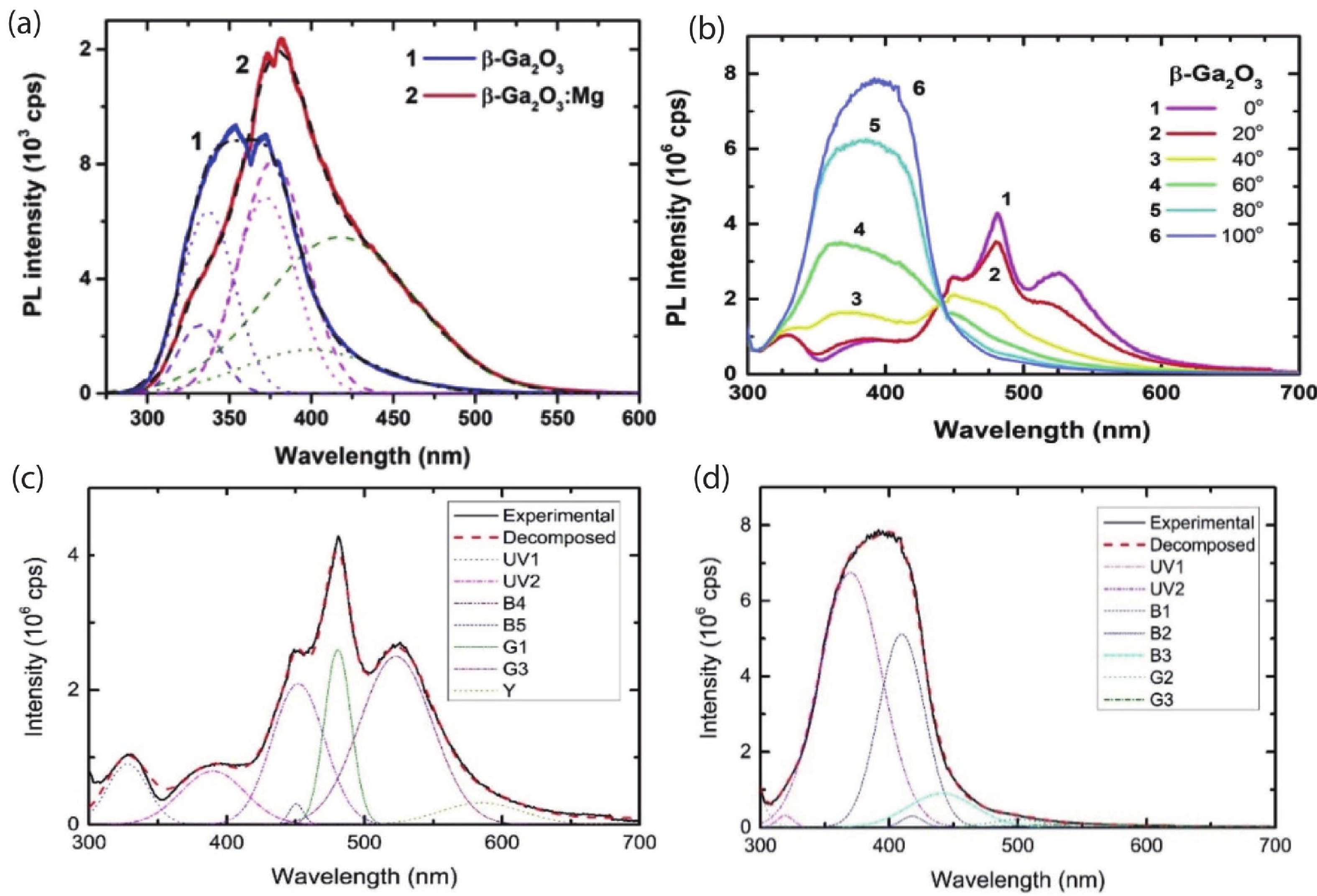
Fig. 5.  (Color online) Anisotropic photoluminescence spectra[37]. (a) Unpolarized and (b) polarized photoluminescence spectra of β-Ga2O3. Gaussian spectral components of photoluminescence at (c) 0° and (d) 100° angle of polarizer. Copyright 2021 by Optica Publishing Group.

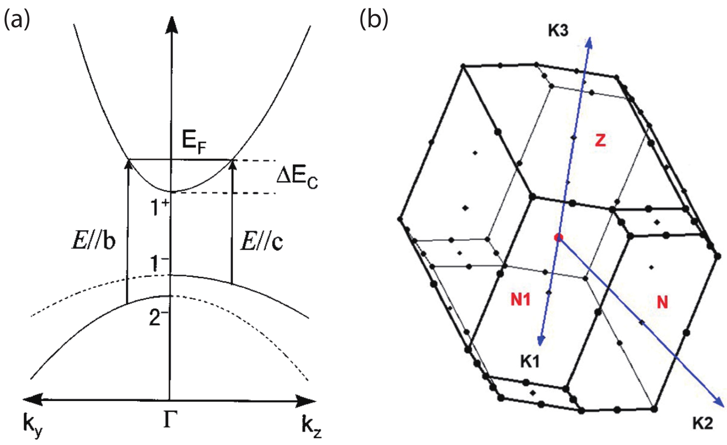
Fig. 6.  (Color online) (a) Schematic diagram of the band structure of β-Ga2O3[31]. Copyright 1997 by AIP publishing. (b) The Brillouin zone of the crystal[45]. Copyright 2016 by AIP publishing.

Fig. 7.  (Color online) (a) Configuration and (b) the photoresponsivity spectra of the narrow-band polarization detector[35]. Copyright 2019 by American Chemical Society. (c) IV characteristics and devie configuration, (d) 2D colour map of photocurrent, (e) normalized photoresponse speed and (f) absorption coefficient along [020] and [202] directions[50]. Copyright 2020 by Royal Society of Chemistry.

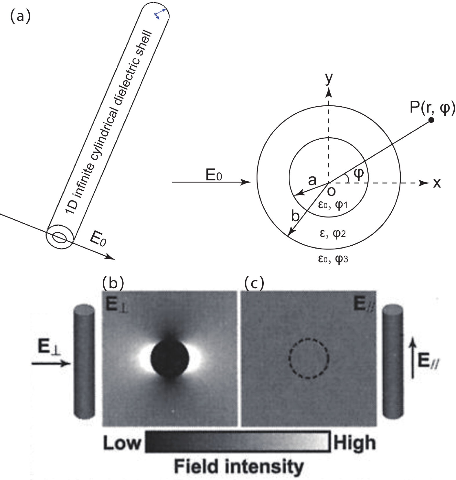
Fig. 8.  (a) Infinite dielectric cylindrical shell in uniform external electric field. Field intensities (|E|2) calculated from Maxwell's when external electric field is (b) perpendicular and (c) parallel to the dielectric object[51]. Copyright 2001 by AAAS.

Fig. 9.  (Color online) Metal-grid polarized photodetector[56]. (a) Schematics of the device structure. (b) SEM image of β-Ga2O3 device. (c) Enlarged view of the metal grid area. (d) Polarization angle response properties of the pristine and MG β-Ga2O3 devices. Copyright 2021 by Elsevier.

Table 1.   Anisotropic bandgaps from literatures.

Ref.MorphologySynthesis methodCharacterizationEg(a)
(eV)
Eg(b)
(eV)
Eg(c) (eV)
[34]Calculation2.3072.9752.478
[33]BulkEFGAbsorption4.574.724.54
[36]BulkEFGTransmittance4.584.734.48
[35]BulkEGGTransmittance4.764.53
[37]BulkFZTransmittance4.864.56
[31]BulkFZTransmittance4.794.52
DownLoad: CSV

Table 2.   The comparison of electrical properties of β-Ga2O3 with AlN, Diamond, GaN and Si. Eg: banggap energy, Ebr: breakdown voltage, K: thermal conductivity, Y: Young's modulus.

Parameter
Eg (eV)Ebr (MV/cm)Velocity (107 cm/s)K (W/(cm·K))Y (GPa)
AlN6.2172.22.9310
Diamond5.5102.7101100
β-Ga2O34.982.40.27230
GaN3.43.32.52.1336
Si1.120.511.56130
DownLoad: CSV

Table 3.   Benchmark of polarization detection reports. (*) represents that the values are calculated by the authors using σ = (IpeakIvalley)/(Ipeak + Ivalley) according to the data in these references, since they are not directly mentioned. (#) represents that the values are recalculated by the authors using σ = (IpeakIvalley)/(Ipeak + Ivalley) in order to reach a unified standard, as they were reported as dichroic ratio using Ipeak / Ivalley.

MaterialCrystal systemAnisotropic planeOptical
bandgap (eV)
Detection wavelengthMaterial morphologyAnisotropic mechanismAnisotropy ratioRef.
β-Ga2O3Monoclinic(−101)4.8UVC3D NanobeltDich. & Morp. & MG0.96(#)[56]
β-Ga2O3Monoclinic(−101)4.8UVC3D NanobeltDichroism0.96(#)[50]
β-Ga2O3Monoclinic(100)4.53-4.76UVC3D BulkDichroism0.53(*)[35]
β-GaxIny03Monoclinic(010)4.4−4.7UVC3D BulkDichroism[57]
GeS2Monoclinic(001)3.71UVA2D flakeDichroism0.36(#)[58]
SnO2Tetragonal(010)3.6UVA3D MicrowireDichroism0.39(#)[59]
MZO/ZnO-MQWHexagonal(11−20)3.17−3.57UVA3D MQWDichroism0.71(#)[60]
ZnOHexagonal(0001)3.37UVA3D Thin filmMG[56]
ZnOHexagonal3.37UVA3D NanowireMorphology0.19(*)[61]
GaNHexagonal(11−20)3.4UVA3D Thin filmDichroism0.76(#)[62]
GaNHexagonal3.4UVA-UVC3D NanowireMorphology0.16[63]
GeSe2Monoclinic(001)2.74VIS2D flakeDichroism0.55(#)[64]
GeSe2Monoclinic(001)2.96VIS2D flakeDichroism0.38(#)[65]
CsPbI3Orthorhombic(100)2.79VIS3D NanowireDich. & Morp.0.46(#)[66]
CdSeCubic & hexagonal1.79VIS3D NanowireMorphology0.13(#)[67]
ZrS3Monoclinic(001)1.79VIS2D nanoribbonDichroism0.27(#)[68]
ReS2/ReSe2Triclinic(001)1.6/1.3VIS2D heterojunctionDichroism0.47(*)[69]
CH3NH3PbI3Tetragonal(001)1.58VIS3D NanowireMorphology0.13(#)[70]
ReS2Triclinic(001)1.5VIS2D flakeDichroism0.47(*)[71]
InpCubic1.35Visible3D NanowireMorphology0.96[51]
TiS3Monoclinic(001)1.13VIS-NIR2D nanoribbonDichroism0.6(#)[72]
GeAs2Orthorhombic(001)1VIS2D flakeDichroism0.33(*)[73]
TlSeTetragonal(110)0.73VIS2D flakeDichroism0.45(#)[74]
BPOrthorhombic(001)0.3VIS-NIR2D flakeDichroism0.82(*)[75]
BPOrthorhombic(001)0.3VIS-MIR2D flakeDichroism0.63(*)[76]
DownLoad: CSV
[1]
Liang H L, Han Z Y, Mei Z X. Recent progress of deep ultraviolet photodetectors using amorphous gallium oxide thin films. Phys Status Solidi A, 2021, 218, 2000339 doi: 10.1002/pssa.202000339
[2]
Kaur D, Kumar M. A strategic review on gallium oxide based deep-ultraviolet photodetectors: Recent progress and future prospects. Adv Optical Mater, 2021, 9, 2002160 doi: 10.1002/adom.202002160
[3]
Atilgan A, Yildiz A, Harmanci U, et al. β-Ga2O3 nanoflakes/p-Si heterojunction self-powered photodiodes. Mater Today Commun, 2020, 24, 101105 doi: 10.1016/j.mtcomm.2020.101105
[4]
Jian L Y, Lee H Y, Lee C T. Ga2O3-based p-i-n solar blind deep ultraviolet photodetectors. J Mater Sci: Mater Electron, 2019, 30, 8445 doi: 10.1007/s10854-019-01163-w
[5]
Zhao B, Wang F, Chen H Y, et al. An ultrahigh responsivity (9.7 mA W–1) self-powered solar-blind photodetector based on individual ZnO-Ga2O3 heterostructures. Adv Funct Mater, 2017, 27, 1700264 doi: 10.1002/adfm.201700264
[6]
Chen M Z, Ma J G, Li P, et al. Zero-biased deep ultraviolet photodetectors based on graphene/cleaved (100) Ga2O3 heterojunction. Opt Express, 2019, 27, 8717 doi: 10.1364/OE.27.008717
[7]
Cui S J, Mei Z X, Zhang Y H, et al. Room-temperature fabricated amorphous Ga2O3 high-response-speed solar-blind photodetector on rigid and flexible substrates. Adv Opt Mater, 2017, 5, 1700454 doi: 10.1002/adom.201700454
[8]
Zhao B, Wang F, Chen H, et al. Solar-blind avalanche photodetector based on single ZnO–Ga2O3 core–shell microwire. Nano Lett, 2015, 15, 3988 doi: 10.1021/acs.nanolett.5b00906
[9]
Han Z Y, Liang H L, Huo W X, et al. Boosted UV photodetection performance in chemically etched amorphous Ga2O3 thin-film transistors. Adv Optical Mater, 2020, 8, 1901833 doi: 10.1002/adom.201901833
[10]
Qin Y, Long S, He Q, et al. Amorphous gallium oxide-based gate-tunable high-performance thin film phototransistor for solar-blind imaging. Adv Electron Mater, 2019, 5, 1900389 doi: 10.1002/aelm.201900389
[11]
Wang Y, Cui W, Yu J, et al. One-step growth of Amorphous/Crystalline Ga2O3 phase junctions for high-performance solar-blind photodetection. ACS Appl Mater Interfaces, 2019, 11, 45922 doi: 10.1021/acsami.9b17409
[12]
Chi Z Y, Asher J J, Jennings M R, et al. Ga2O3 and related ultra-wide bandgap power semiconductor oxides: New energy electronics solutions for CO2 emission mitigation. Materials, 2022, 15, 1164 doi: 10.3390/ma15031164
[13]
Hu Z, Zhou H, Feng Q, et al. Field-plated lateral β-Ga2O3 Schottky barrier diode with high reverse blocking voltage of more than 3 kV and high DC power figure-of-merit of 500 MW/cm2. IEEE Electron Device Lett, 2018, 39, 1564 doi: 10.1109/LED.2018.2868444
[14]
Sharma S, Zeng K, Saha S, et al. Field-plated lateral Ga2O3 MOSFETs with polymer passivation and 8.03 kV breakdown voltage. IEEE Electron Device Lett, 2020, 41, 836 doi: 10.1109/LED.2020.2991146
[15]
Sui Y X, Liang H L, Chen Q S, et al. Room-temperature ozone sensing capability of IGZO-decorated amorphous Ga2O3 films. ACS Appl Mater Interfaces, 2020, 12, 8929 doi: 10.1021/acsami.9b22400
[16]
Liang H, Cui S, Su R, et al. Flexible X-ray detectors based on amorphous Ga2O3 thin films. ACS Photonics, 2018, 6, 351 doi: 10.1021/acsphotonics.8b00769
[17]
Geller S. Crystal structure of β-Ga2O3. J Chem Phys, 1960, 33, 676 doi: 10.1063/1.1731237
[18]
Lorenz M R, Woods J F, Gambino R J. Some electrical properties of the semiconductor β-Ga2O3. J Phys Chem Solids, 1967, 28, 403 doi: 10.1016/0022-3697(67)90305-8
[19]
Li L, Han W, Pi L, et al. Emerging in-plane anisotropic two-dimensional materials. InfoMat, 2019, 1, 54 doi: 10.1002/inf2.12005
[20]
Binet L, Gourier D. Origin of the blue luminescence of β-Ga2O3. J Phys Chem Solids, 1998, 59, 1241 doi: 10.1016/S0022-3697(98)00047-X
[21]
Binet L, Gourier D, Minot C. Relation between electron band structure and magnetic bistability of conduction electrons in β-Ga2O3. J Solid State Chem, 1994, 113, 420 doi: 10.1006/jssc.1994.1390
[22]
Hwang W S, Verma A, Peelaers H, et al. High-voltage field effect transistors with wide-bandgap β-Ga2O3 nanomembranes. Appl Phys Lett, 2014, 104, 203111 doi: 10.1063/1.4879800
[23]
Åhman J, Svensson G, Albertsson J. A reinvestigation of β-gallium oxide. Acta Crystallogr C, 1996, 52, 1336 doi: 10.1107/S0108270195016404
[24]
Oh S, Mastro M A, Tadjer M J, et al. Solar-blind metal-semiconductor-metal photodetectors based on an exfoliated β-Ga2O3 Micro-flake. ECS J Solid State Sci Technol, 2017, 6, Q79 doi: 10.1149/2.0231708jss
[25]
Liu X L, Zhang X, Lin M L, et al. Different angle-resolved polarization configurations of Raman spectroscopy: A case on the basal and edge plane of two-dimensional materials. Chin Phys B, 2017, 26, 067802 doi: 10.1088/1674-1056/26/6/067802
[26]
Li Z, Liu Y, Zhang A, et al. Quasi-two-dimensional β-Ga2O3 field effect transistors with large drain current density and low contact resistance via controlled formation of interfacial oxygen vacancies. Nano Res, 2019, 12, 143 doi: 10.1007/s12274-018-2193-7
[27]
Chen J X, Li X X, Huang W, et al. High-energy X-ray radiation effects on the exfoliated quasi-two-dimensional β-Ga2O3 nanoflake field-effect transistors. Nanotechnology, 2020, 31, 345206 doi: 10.1088/1361-6528/ab925d
[28]
Bae J, Kim H W, Kang I H, et al. High breakdown voltage quasi-two-dimensional β-Ga2O3 field-effect transistors with a boron nitride field plate. Appl Phys Lett, 2018, 112, 122102 doi: 10.1063/1.5018238
[29]
Kwon Y, Lee G, Oh S, et al. Tuning the thickness of exfoliated quasi-two-dimensional β-Ga2O3 flakes by plasma etching. Appl Phys Lett, 2017, 110, 131901 doi: 10.1063/1.4979028
[30]
Kim J, Mastro M A, Tadjer M J, et al. Quasi-two-dimensional h-BN/β-Ga2O3 heterostructure metal-insulator-semiconductor field-effect transistor. ACS Appl Mater Interfaces, 2017, 9, 21322 doi: 10.1021/acsami.7b04374
[31]
Ueda N, Hosono H, Waseda R, et al. Anisotropy of electrical and optical properties in β-Ga2O3 single crystals. Appl Phys Lett, 1997, 71, 933 doi: 10.1063/1.119693
[32]
Varley J B, Weber J R, Janotti A, et al. Oxygen vacancies and donor impurities in β-Ga2O3. Appl Phys Lett, 2010, 97, 142106 doi: 10.1063/1.3499306
[33]
Ricci F, Boschi F, Baraldi A, et al. Theoretical and experimental investigation of optical absorption anisotropy in β-Ga2O3. J Phys:Conden Matter, 2016, 28, 224005 doi: 10.1088/0953-8984/28/22/224005
[34]
Yamaguchi K. First principles study on electronic structure of β-Ga2O3. Solid State Commun, 2004, 131, 739 doi: 10.1016/j.ssc.2004.07.030
[35]
Chen X, Mu W, Xu Y, et al. Highly narrow-band polarization-sensitive solar-blind photodetectors based on β-Ga2O3 single crystals. ACS Appl Mater Interfaces, 2019, 11, 7131 doi: 10.1021/acsami.8b19524
[36]
Mu W, Chen X, He G, et al. Anisotropy and in-plane polarization of low-symmetrical β-Ga2O3 single crystal in the deep ultraviolet band. Appl Surf Sci, 2020, 527, 146648 doi: 10.1016/j.apsusc.2020.146648
[37]
Zhang N J, Kislyakov I M, Xia C T, et al. Anisotropic luminescence and third-order electric susceptibility of Mg-doped gallium oxide under the half-bandgap edge. Opt Express, 2021, 29, 18587 doi: 10.1364/OE.427021
[38]
Bilbao Crystallographic Server, https://www.cryst.ehu.es/ (accessed August 15, 2022)
[39]
Kranert C, Sturm C, Schmidt-Grund R, et al. Raman tensor elements of β-Ga2O3. Sci Rep, 2016, 6, 1 doi: 10.1038/s41598-016-0001-8
[40]
Jones R C. A new calculus for the treatment of optical SystemsI description and discussion of the calculus. J Opt Soc Am, 1941, 31, 488 doi: 10.1364/JOSA.31.000488
[41]
Frodason Y K, Johansen K M, Vines L, et al. Self-trapped hole and impurity-related broad luminescence in β-Ga2O3. J Appl Phys, 2020, 127, 075701 doi: 10.1063/1.5140742
[42]
Marcinkevičius S, Speck J S. Ultrafast dynamics of hole self-localization in β-Ga2O3. Appl Phys Lett, 2020, 116, 132101 doi: 10.1063/5.0003682
[43]
Yang J C, Ren F, Tadjer M, et al. 2300V reverse breakdown voltage Ga2O3Schottky rectifiers. ECS J Solid State Sci Technol, 2018, 7, Q92 doi: 10.1149/2.0241805jss
[44]
Wong M H, Sasaki K, Kuramata A, et al. Field-plated Ga2O3 MOSFETs with a breakdown voltage of over 750 V. IEEE Electron Device Lett, 2016, 37, 212 doi: 10.1109/LED.2015.2512279
[45]
Ghosh K, Singisetti U. Ab initio calculation of electron-phonon coupling in monoclinic β-Ga2O3 crystal. Appl Phys Lett, 2016, 109, 072102 doi: 10.1063/1.4961308
[46]
Ghosh K, Singisetti U. Low-field and high-field transport in β-Ga2O3. In: Gallium Oxide. Elsevier, 2019
[47]
Li Z, Wang Q, Feng C, et al. Simulation study of performance degradation in β-Ga2O3 (001) vertical Schottky barrier diodes based on anisotropic mobility modeling. ECS J Solid State Sci Technol, 2021, 10, 055005 doi: 10.1149/2162-8777/abed98
[48]
Higashiwaki M, Konishi K, Sasaki K, et al. Temperature-dependent capacitance–voltage and current–voltage characteristics of Pt/Ga2O3 (001) Schottky barrier diodes fabricated on n–Ga2O3 drift layers grown by halide vapor phase epitaxy. Appl Phys Lett, 2016, 108, 133503 doi: 10.1063/1.4945267
[49]
Vavoulas A, Sandalidis H G, Chatzidiamantis N D, et al. A survey on ultraviolet C-band (UV-C) communications. IEEE Commun Surv Tutorials, 2019, 21, 2111 doi: 10.1109/COMST.2019.2898946
[50]
Chen Q, Zhang Y H, Zheng T, et al. Polarization detection in deep-ultraviolet light with monoclinic gallium oxide nanobelts. Nanoscale Adv, 2020, 2, 2705 doi: 10.1039/D0NA00364F
[51]
Wang J F, Gudiksen M S, Duan X F, et al. Highly polarized photoluminescence and photodetection from single indium phosphide nanowires. Science, 2001, 293, 1455 doi: 10.1126/science.1062340
[52]
Soria E, Gomez-Rodriguez P, Tromas C, et al. Self-assembled, 10 nm-tailored, near infrared plasmonic metasurface acting as broadband omnidirectional polarizing mirror. Adv Opt Mater, 2020, 8, 2000321 doi: 10.1002/adom.202000321
[53]
Oh S, Lee J H, Lee H J, et al. Polarized ultraviolet emitters with Al wire-grid polarizers fabricated by solvent-assisted nanotransfer process. Nanotechnology, 2019, 31, 045304 doi: 10.1088/1361-6528/ab4c16
[54]
Sun D, Feng B, Yang B, et al. Design and fabrication of an InGaAs focal plane array integrated with linear-array polarization grating. Opt Lett, 2020, 45, 1559 doi: 10.1364/OL.376110
[55]
Freitas Carvalho F, Augusto de Moraes Cruz C, Costa Marques G, et al. Angular light, polarization and stokes parameters information in a hybrid image sensor with division of focal plane. Sensors, 2020, 20, 3391 doi: 10.3390/s20123391
[56]
Zhang Y H, Wang Z X, Xing F. Enhancement of polarization response in UVA and UVC wavelength with integrated sub-wavelength metal-grids. Microelectron Eng, 2021, 242/243, 111555 doi: 10.1016/j.mee.2021.111555
[57]
Vasyltsiv V I, Rym Y I, Zakharko Y M. Optical absorption and photoconductivity at the band edge of β-Ga2–xInxO3. Phys Stat Sol B, 1996, 195, 653 doi: 10.1002/pssb.2221950232
[58]
Yang Y, Liu S C, Wang X, et al. Polarization-sensitive ultraviolet photodetection of anisotropic 2D GeS2. Adv Funct Mater, 2019, 29, 1900411 doi: 10.1002/adfm.201900411
[59]
Li L, Gao W, Chen H Y, et al. Strong anisotropy and piezo-phototronic effect in SnO2 microwires. Adv Electron Mater, 2020, 6, 1901441 doi: 10.1002/aelm.201901441
[60]
Tabares G, Hierro A, Vinter B, et al. Polarization-sensitive Schottky photodiodes based on a-plane ZnO/ZnMgO multiple quantum-wells. Appl Phys Lett, 2011, 99, 071108 doi: 10.1063/1.3624924
[61]
Fan Z, Chang P C, Lu J G, et al. Photoluminescence and polarized photodetection of single ZnO nanowires. Appl Phys Lett, 2004, 85, 6128 doi: 10.1063/1.1841453
[62]
Rivera C, Pau J L, Muñoz E, et al. Polarization-sensitive ultraviolet photodetectors based on M-plane GaN grown on LiAlO2 substrates. Appl Phys Lett, 2006, 88, 213507 doi: 10.1063/1.2206128
[63]
Han S, Jin W, Zhang D H, et al. Photoconduction studies on GaN nanowire transistors under UV and polarized UV illumination. Chem Phys Lett, 2004, 389, 176 doi: 10.1016/j.cplett.2004.03.083
[64]
Yang Y, Liu S C, Yang W, et al. Air-stable in-plane anisotropic GeSe2 for highly polarization-sensitive photodetection in short wave region. J Am Chem Soc, 2018, 140, 4150 doi: 10.1021/jacs.8b01234
[65]
Yan Y, Xiong W, Li S, et al. Direct wide bandgap 2D GeSe2 monolayer toward anisotropic UV photodetection. Adv Optl Mater, 2019, 7, 1900622 doi: 10.1002/adom.201900622
[66]
Zhou Y, Luo J, Zhao Y, et al. Flexible linearly polarized photodetectors based on all-inorganic perovskite CsPbI3 nanowires. Adv Opt Mater, 2018, 6, 1800679 doi: 10.1002/adom.201800679
[67]
Singh A, Li X, Protasenko V, et al. Polarization-sensitive nanowire photodetectors based on solution-synthesized CdSe quantum-wire solids. Nano Lett, 2007, 7, 2999 doi: 10.1021/nl0713023
[68]
Wang X, Wu K, Blei M, et al. Highly polarized photoelectrical response in vdW ZrS3 nanoribbons. Adv Electron Mater, 2019, 5, 1900419 doi: 10.1002/aelm.201900419
[69]
Liu D, Hong J, Wang X, et al. Diverse atomically sharp interfaces and linear dichroism of 1T'ReS2-ReSe2 lateral p–n heterojunctions. Adv Funct Mater, 2018, 28, 1804696 doi: 10.1002/adfm.201804696
[70]
Gao L, Zeng K, Guo J, et al. Passivated single-crystalline CH3NH3PbI3 nanowire photodetector with high detectivity and polarization sensitivity. Nano Lett, 2016, 16(12), 7446 doi: 10.1021/acs.nanolett.6b03119
[71]
Liu F, Zheng S, He X, et al. Highly sensitive detection of polarized light using anisotropic 2D ReS2. Adv Funct Mater, 2016, 26, 1169 doi: 10.1002/adfm.201504546
[72]
Liu S, Xiao W, Zhong M, et al. Highly polarization sensitive photodetectors based on quasi-1D titanium trisulfide (TiS3). Nanotechnology, 2018, 29, 184002 doi: 10.1088/1361-6528/aaafa2
[73]
Li L, Gong P, Sheng D, et al. Highly in-plane anisotropic 2D GeAs2 for polarization-sensitive photodetection. Adv Mater, 2018, 30, 1804541 doi: 10.1002/adma.201804541
[74]
Yang S, Hu C, Wu M, et al. In-plane optical anisotropy and linear dichroism in low-symmetry layered TlSe. ACS Nano, 2018, 12, 8798 doi: 10.1021/acsnano.8b05162
[75]
Hong T, Chamlagain B, Wang T J, et al. Anisotropic photocurrent response at black phosphorus-MoS2 p–n heterojunctions. Nanoscale, 2015, 7, 18537 doi: 10.1039/C5NR03400K
[76]
Yuan H, Liu X, Afshinmanesh F, et al. Polarization-sensitive broadband photodetector using a black phosphorus vertical p–n junction. Nat Nanotechnol, 2015, 10, 707 doi: 10.1038/nnano.2015.112
[77]
Mitdank R, Dusari S, Bülow C, et al. Temperature-dependent electrical characterization of exfoliated β-Ga2O3 micro flakes. Phys Status Solidi A, 2014, 211, 543 doi: 10.1002/pssa.201330671
[78]
Kim J, Oh S, Mastro M A, et al. Exfoliated β-Ga2O3 nano-belt field-effect transistors for air-stable high power and high temperature electronics. Phys Chem Chem Phys, 2016, 18, 15760 doi: 10.1039/C6CP01987K
[79]
Guo Z, Verma A, Wu X, et al. Anisotropic thermal conductivity in single crystal β-gallium oxide. Appl Phys Lett, 2015, 106, 111909 doi: 10.1063/1.4916078
[80]
Handwerg M, Mitdank R, Galazka Z, et al. Temperature-dependent thermal conductivity in Mg-doped and undoped β-Ga2O3 bulk-crystals. Semicond Sci Technol, 2015, 30, 024006 doi: 10.1088/0268-1242/30/2/024006
  • Search

    Advanced Search >>

    GET CITATION

    shu

    Export: BibTex EndNote

    Article Metrics

    Article views: 1303 Times PDF downloads: 221 Times Cited by: 0 Times

    History

    Received: 22 November 2022 Revised: 27 December 2022 Online: Accepted Manuscript: 18 February 2023Uncorrected proof: 20 February 2023Corrected proof: 12 June 2023Published: 10 July 2023

    Catalog

      Email This Article

      User name:
      Email:*请输入正确邮箱
      Code:*验证码错误
      Yonghui Zhang, Fei Xing. Anisotropic optical and electric properties of β-gallium oxide[J]. Journal of Semiconductors, 2023, 44(7): 071801. doi: 10.1088/1674-4926/44/7/071801 ****Yonghui Zhang, Fei Xing. 2023: Anisotropic optical and electric properties of β-gallium oxide. Journal of Semiconductors, 44(7): 071801. doi: 10.1088/1674-4926/44/7/071801
      Citation:
      Yonghui Zhang, Fei Xing. Anisotropic optical and electric properties of β-gallium oxide[J]. Journal of Semiconductors, 2023, 44(7): 071801. doi: 10.1088/1674-4926/44/7/071801 ****
      Yonghui Zhang, Fei Xing. 2023: Anisotropic optical and electric properties of β-gallium oxide. Journal of Semiconductors, 44(7): 071801. doi: 10.1088/1674-4926/44/7/071801

      Anisotropic optical and electric properties of β-gallium oxide

      DOI: 10.1088/1674-4926/44/7/071801
      More Information
      • Yonghui Zhang:obtained his PhD degree in condensed matter physics from the Institute of Physics, Chinese Academy of Sciences in 2018. His research interests include flexible transparent electronic, oxide semiconductors and high-voltage devices. Currently, he works in the School of Physics and Optoelectronics Engineering in Shandong University of Technology
      • Fei Xing:got his PhD degree from Nankai University in optics in 2014. His research interests are the optical properties of graphene-based total internal reflection devices. Now, he works in the School of Physics and Optoelectronic Engineering in Shandong University of Technology, mainly engaged in the application of low-dimensional semiconductor materials and optical devices
      • Corresponding author: yhzhang@sdut.edu.cnxingfei@sdut.edu.cn
      • Received Date: 2022-11-22
      • Revised Date: 2022-12-27
      • Available Online: 2023-02-18

      Catalog

        /

        DownLoad:  Full-Size Img  PowerPoint
        Return
        Return