


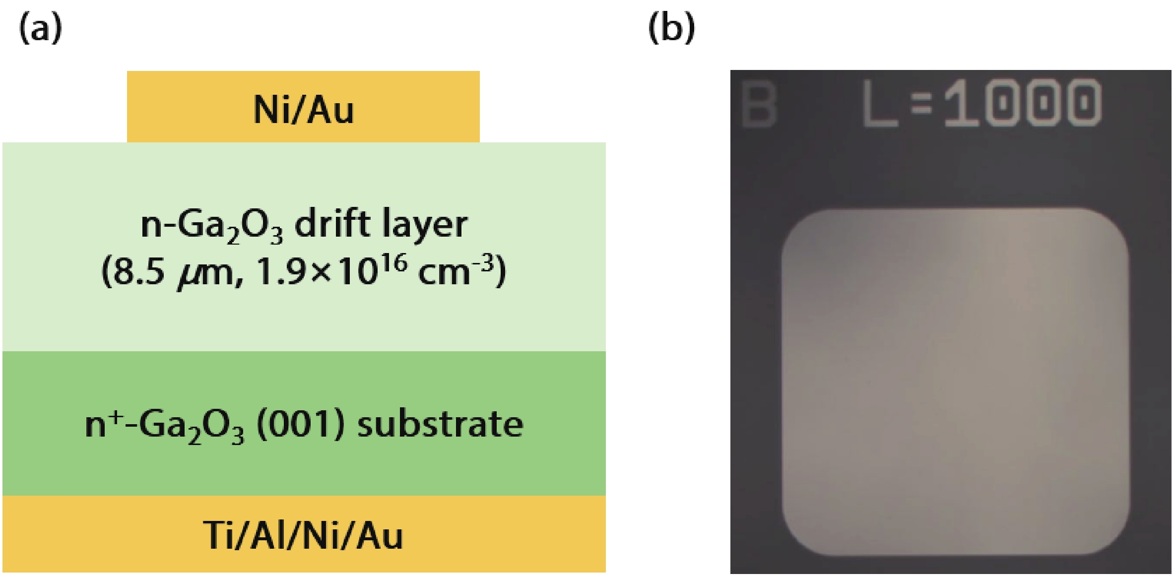
Fig. 1.
(Color online) (a) Schematic cross section of the β-Ga2O3 SBD. (b) Optical image.
ARTICLES
Wei Guo, Zhao Han, Xiaolong Zhao, Guangwei Xu and Shibing Long
Corresponding author: Guangwei Xu, xugw@ustc.edu.cn; Shibing Long, shibinglong@ustc.edu.cn
Abstract: We demonstrate superb large-area vertical β-Ga2O3 SBDs with a Schottky contact area of 1 × 1 mm2 and obtain a high-efficiency DC–DC converter based on the device. The β-Ga2O3 SBD can obtain a forward current of 8 A with a forward voltage of 5 V, and has a reverse breakdown voltage of 612 V. The forward turn-on voltage (VF) and the on-resistance (Ron) are 1.17 V and 0.46 Ω, respectively. The conversion efficiency of the β-Ga2O3 SBD-based DC–DC converter is 95.81%. This work indicates the great potential of Ga2O3 SBDs and relevant circuits in power electronic applications.
Keywords: β-Ga2O3, SBD, DC–DC converter
| [1] |
Baliga B J. Fundamentals of power semiconductor devices. Cham: Springer International Publishing, 2019
|
| [2] |
Sasaki K, Higashiwaki M, Kuramata A, et al. Ga2O3 Schottky barrier diodes fabricated by using single-crystal β–Ga2O3 (010) substrates. IEEE Electron Device Lett, 2013, 34, 493 doi: 10.1109/LED.2013.2244057
|
| [3] |
Higashiwaki M, Sasaki K, Kuramata A, et al. Gallium oxide (Ga2O3) metal-semiconductor field-effect transistors on single-crystal β-Ga2O3 (010) substrates. Appl Phys Lett, 2012, 100, 013504 doi: 10.1063/1.3674287
|
| [4] |
Pearton S J, Yang J C, Cary P H IV, et al. A review of Ga2O3 materials, processing, and devices. Appl Phys Rev, 2018, 5, 011301 doi: 10.1063/1.5006941
|
| [5] |
Pearton S J, Ren F, Tadjer M, et al. Perspective: Ga2O3 for ultra-high power rectifiers and MOSFETS. J Appl Phys, 2018, 124, 220901 doi: 10.1063/1.5062841
|
| [6] |
Ren F, Yang J C, Fares C, et al. Device processing and junction formation needs for ultra-high power Ga2O3 electronics. MRS Commun, 2019, 9, 77 doi: 10.1557/mrc.2019.4
|
| [7] |
Konishi K, Goto K, Murakami H, et al. 1-kV vertical Ga2O3 field-plated Schottky barrier diodes. Appl Phys Lett, 2017, 110, 103506 doi: 10.1063/1.4977857
|
| [8] |
Zhou H, Yan Q L, Zhang J C, et al. High-performance vertical β-Ga2O3 Schottky barrier diode with implanted edge termination. IEEE Electron Device Lett, 2019, 40, 1788 doi: 10.1109/LED.2019.2939788
|
| [9] |
Ji M, Taylor N R, Kravchenko I, et al. Demonstration of large-size vertical Ga2O3 Schottky barrier diodes. IEEE Trans Power Electron, 2020, 36, 41 doi: 10.1109/TPEL.2020.3001530
|
| [10] |
Li W S, Nomoto K, Hu Z Y, et al. Field-plated Ga2O3 trench Schottky barrier diodes with a BV2/ Ron, sp of up to 0.95 GW/cm2. IEEE Electron Device Lett, 2020, 41, 107 doi: 10.1109/LED.2019.2953559
|
| [11] |
He Q M, Hao W B, Zhou X Z, et al. Over 1 GW/cm2 vertical Ga2O3 Schottky barrier diodes without edge termination. IEEE Electron Device Lett, 2022, 43, 264 doi: 10.1109/LED.2021.3133866
|
| [12] |
Yang J C, Ren F, Chen Y T, et al. Dynamic switching characteristics of 1 A forward current β-Ga2O3 rectifiers. IEEE J Electron Devices Soc, 2018, 7, 57 doi: 10.1109/JEDS.2018.2877495
|
| [13] |
Lv Y J, Wang Y G, Fu X C, et al. Demonstration of β-Ga2O3 junction barrier Schottky diodes with a Baliga’s figure of merit of 0.85 GW/cm2 or a 5A/700 V handling capabilities. IEEE Trans Power Electron, 2021, 36, 6179 doi: 10.1109/TPEL.2020.3036442
|
| [14] |
Otsuka F, Miyamoto H, Takatsuka A, et al. Large-size (1.7 × 1.7 mm2) β-Ga2O3 field-plated trench MOS-type Schottky barrier diodes with 1.2 kV breakdown voltage and 109 high on/off current ratio. Appl Phys Exp, 2022, 15, 016501 doi: 10.35848/1882-0786/ac4080
|
| [15] |
Hao W B, Wu F H, Li W S, et al. High-performance vertical β- Ga2O3 Schottky barrier diodes featuring P-NiO JTE with adjustable conductivity. 2022 International Electron Devices Meeting (IEDM). San Francisco, CA, USA. IEEE, 2023, 9.5.1 doi: 10.1109/IEDM45625.2022.10019468
|
| [16] |
Guo W, Jian G Z, Hao W B, et al. β-Ga2O3 field plate Schottky barrier diode with superb reverse recovery for high-efficiency DC–DC converter. IEEE J Electron Devices Soc, 2022, 10, 933 doi: 10.1109/JEDS.2022.3212368
|
| [17] |
Wei Y X, Luo X R, Wang Y G, et al. Experimental study on static and dynamic characteristics of Ga2O3 Schottky barrier diodes with compound termination. IEEE Trans Power Electron, 2021, 36, 10976 doi: 10.1109/TPEL.2021.3069918
|
| [18] |
Yang J C, Fares C, Elhassani R, et al. Reverse breakdown in large area, field-plated, vertical β-Ga2O3 rectifiers. ECS J Solid State Sci Technol, 2019, 8, Q3159 doi: 10.1149/2.0211907jss
|
| [19] |
Sharma R, Xian M H, Fares C, et al. Effect of probe geometry during measurement of >100 A Ga2O3 vertical rectifiers. J Vac Sci Technol A, 2021, 39, 013406 doi: 10.1116/6.0000815
|
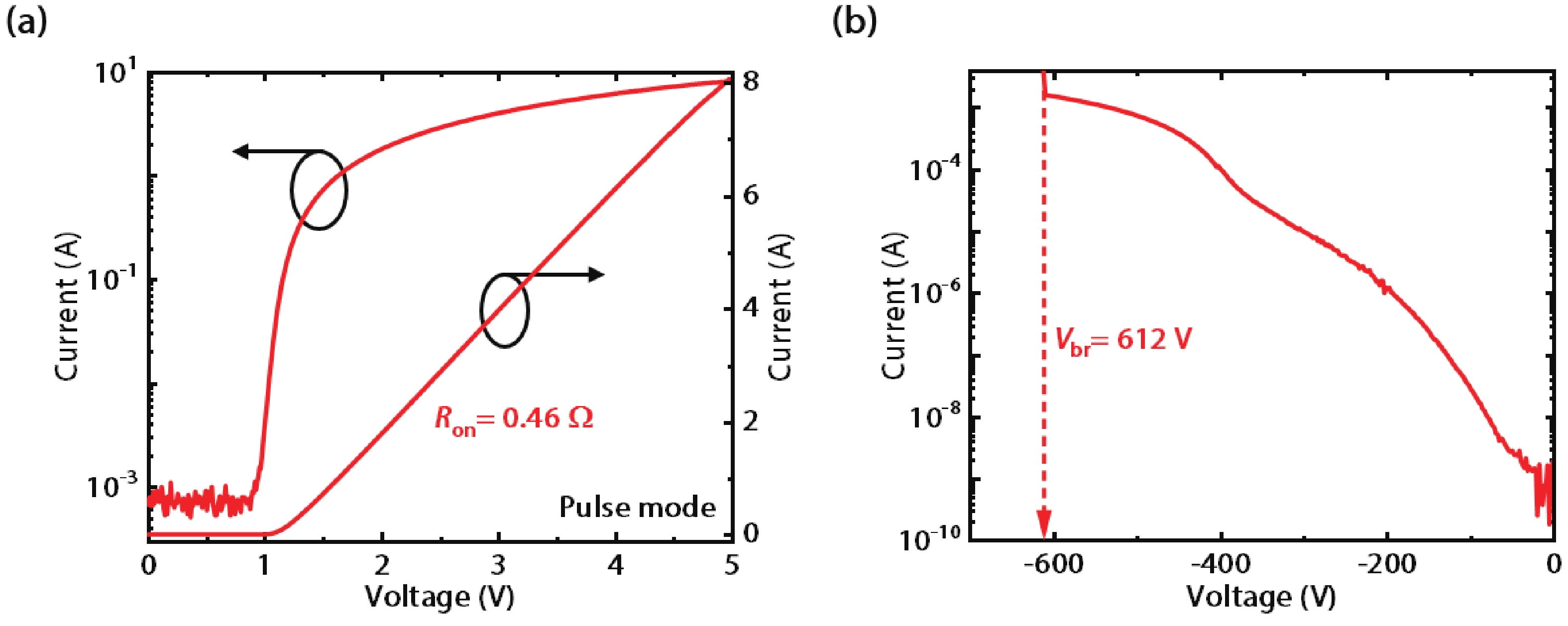
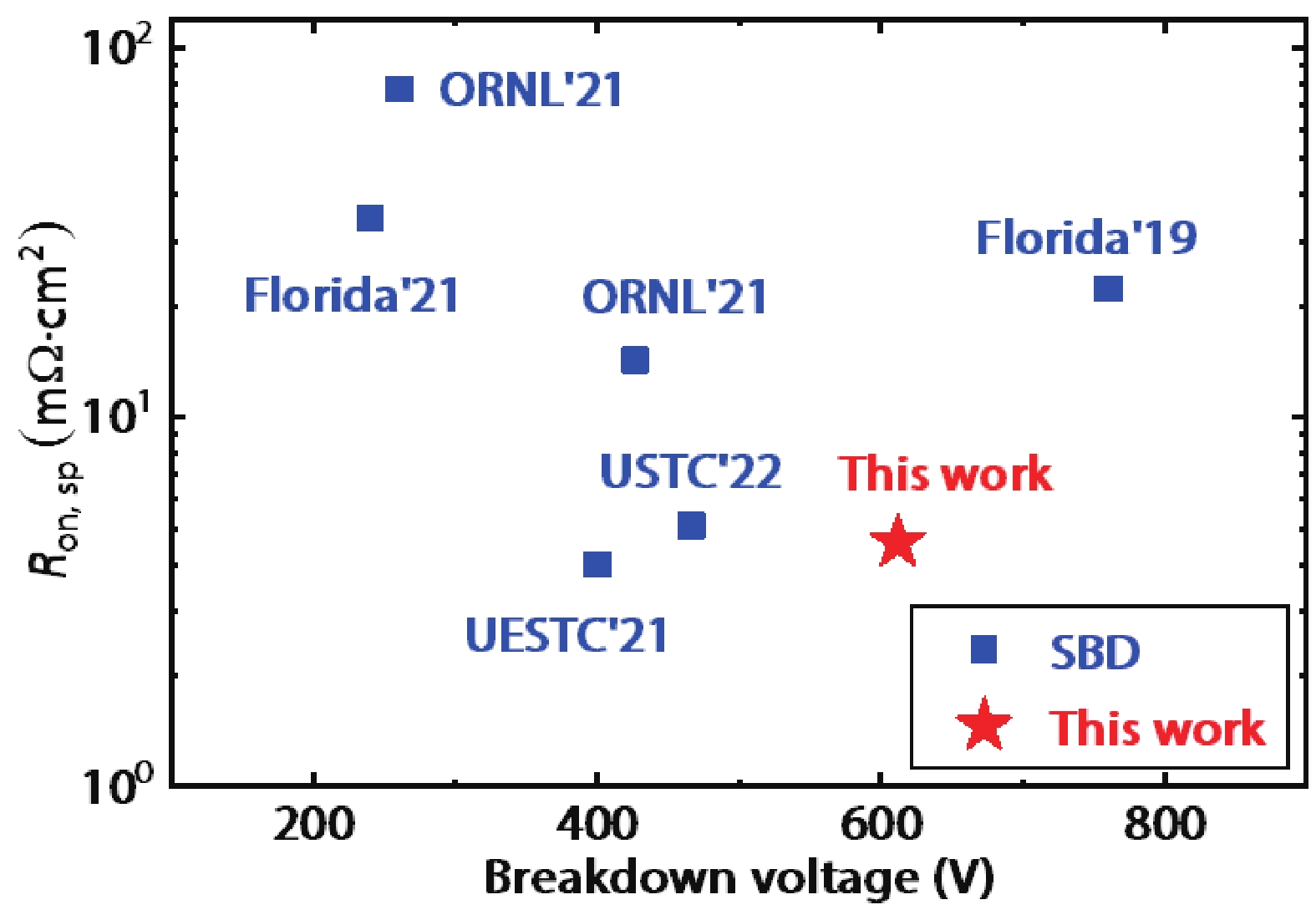
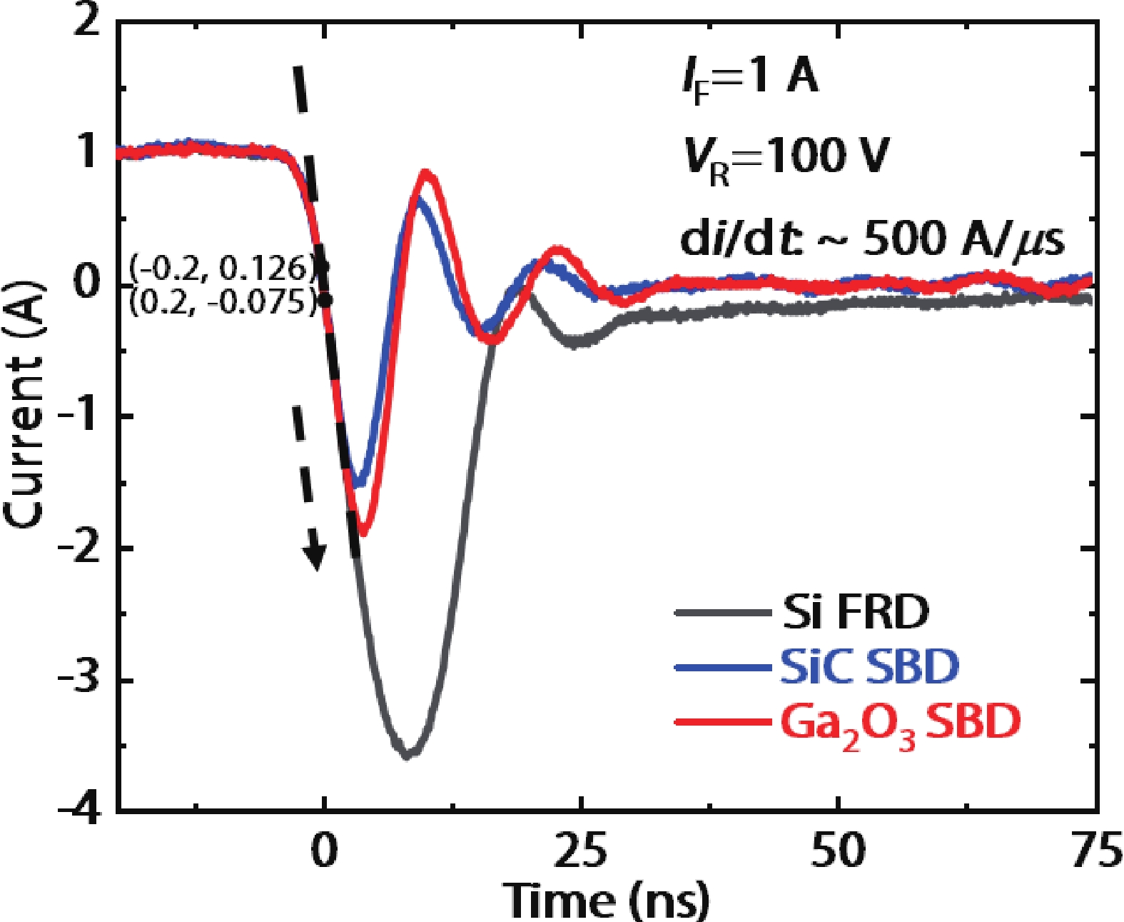
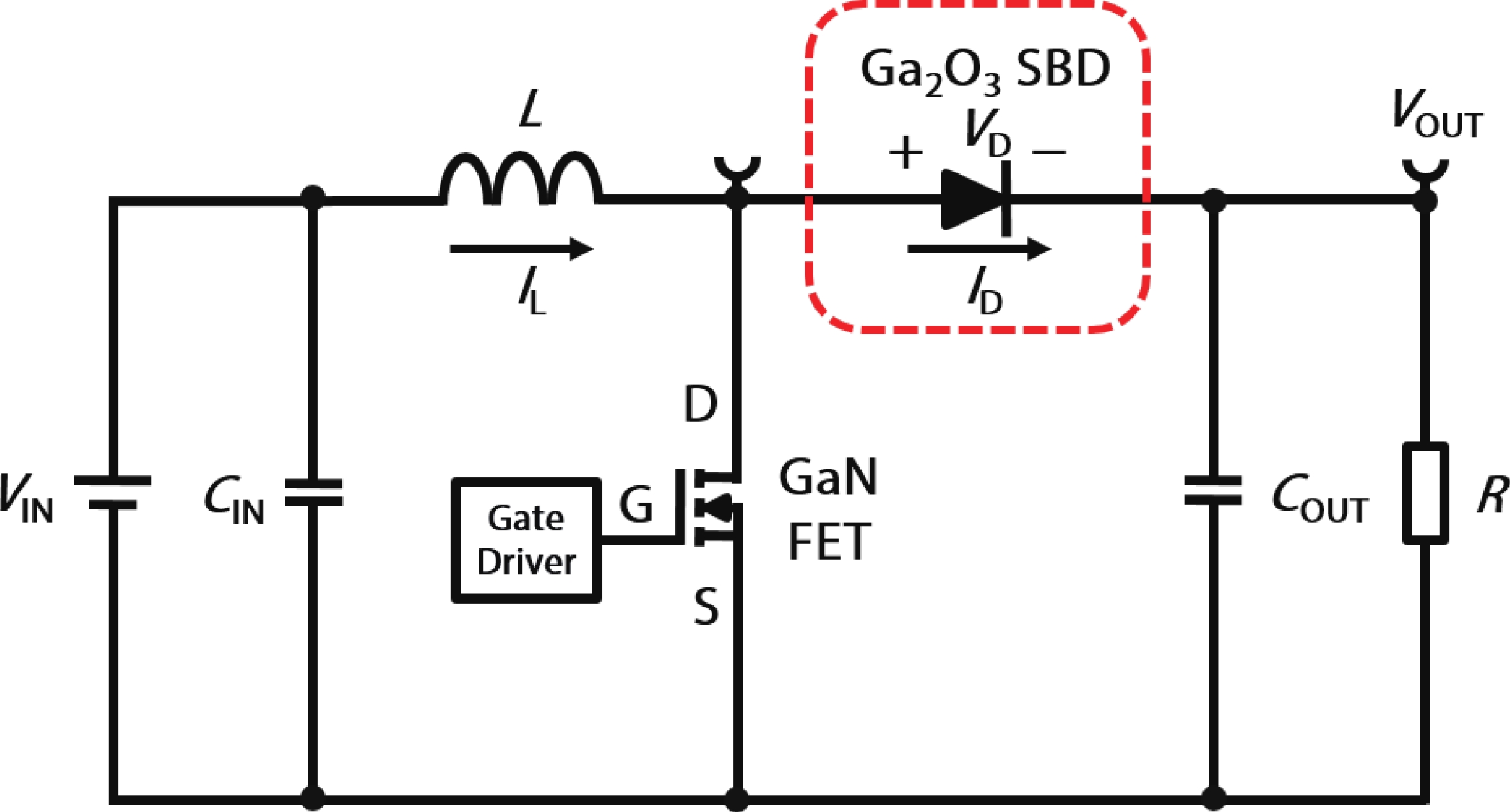
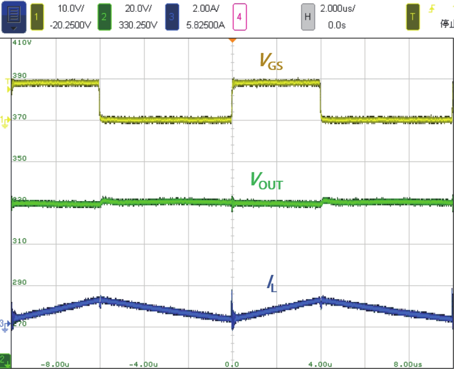
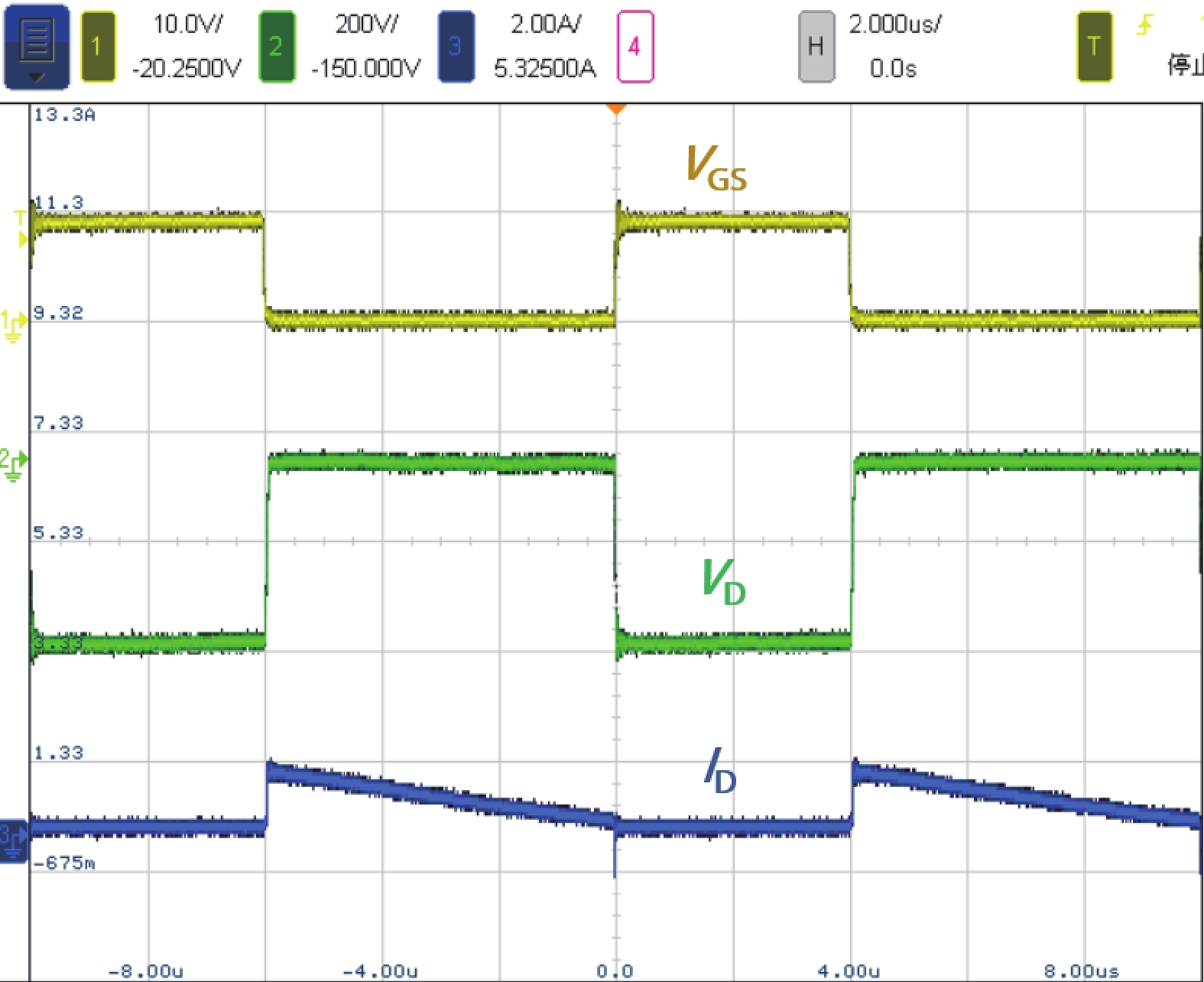
Table 1. Properties of the β-Ga2O3 with commercial Si and SiC devices.
| Parameters | Si FRD | SiC SBD | β-Ga2O3 SBD |
| Ron (Ω) | 0.17 | 0.38 | 0.46 |
| Vbr (V) | 663 | 776 | 612 |
| Irr (A) | 3.61 | 1.54 | 1.9 |
| trr (ns) | 16.9 | 6.8 | 7.4 |
| Qrr (nC) | 38.34 | 6.50 | 8.69 |
 DownLoad: CSV
Table 2. Specifications of the DC-DC converter.
| Parameters | Values | Parameters | Values | |
| GaN FET | 650 V/180 mΩ | L (mH) | 1 | |
| VIN (V) | 200 | f (kHz) | 100 | |
| CIN@315 V (μF) | 100 | D | 40% | |
| COUT@500 V (μF) | 6.8 | R (kΩ) | 1 |
DownLoad: CSV
Table 3. Experimental results of the DC-DC converter.
| Parameters | Values | Parameters | Values | |
| VIN (V) | 200 | PIN (W) | 115.28 | |
| VAUX (V) | 9 | POUT (W) | 110.45 | |
| VOUT (V) | 329.7 | Efficiency | 95.81% |
DownLoad: CSV
| [1] |
Baliga B J. Fundamentals of power semiconductor devices. Cham: Springer International Publishing, 2019
|
| [2] |
Sasaki K, Higashiwaki M, Kuramata A, et al. Ga2O3 Schottky barrier diodes fabricated by using single-crystal β–Ga2O3 (010) substrates. IEEE Electron Device Lett, 2013, 34, 493 doi: 10.1109/LED.2013.2244057
|
| [3] |
Higashiwaki M, Sasaki K, Kuramata A, et al. Gallium oxide (Ga2O3) metal-semiconductor field-effect transistors on single-crystal β-Ga2O3 (010) substrates. Appl Phys Lett, 2012, 100, 013504 doi: 10.1063/1.3674287
|
| [4] |
Pearton S J, Yang J C, Cary P H IV, et al. A review of Ga2O3 materials, processing, and devices. Appl Phys Rev, 2018, 5, 011301 doi: 10.1063/1.5006941
|
| [5] |
Pearton S J, Ren F, Tadjer M, et al. Perspective: Ga2O3 for ultra-high power rectifiers and MOSFETS. J Appl Phys, 2018, 124, 220901 doi: 10.1063/1.5062841
|
| [6] |
Ren F, Yang J C, Fares C, et al. Device processing and junction formation needs for ultra-high power Ga2O3 electronics. MRS Commun, 2019, 9, 77 doi: 10.1557/mrc.2019.4
|
| [7] |
Konishi K, Goto K, Murakami H, et al. 1-kV vertical Ga2O3 field-plated Schottky barrier diodes. Appl Phys Lett, 2017, 110, 103506 doi: 10.1063/1.4977857
|
| [8] |
Zhou H, Yan Q L, Zhang J C, et al. High-performance vertical β-Ga2O3 Schottky barrier diode with implanted edge termination. IEEE Electron Device Lett, 2019, 40, 1788 doi: 10.1109/LED.2019.2939788
|
| [9] |
Ji M, Taylor N R, Kravchenko I, et al. Demonstration of large-size vertical Ga2O3 Schottky barrier diodes. IEEE Trans Power Electron, 2020, 36, 41 doi: 10.1109/TPEL.2020.3001530
|
| [10] |
Li W S, Nomoto K, Hu Z Y, et al. Field-plated Ga2O3 trench Schottky barrier diodes with a BV2/ Ron, sp of up to 0.95 GW/cm2. IEEE Electron Device Lett, 2020, 41, 107 doi: 10.1109/LED.2019.2953559
|
| [11] |
He Q M, Hao W B, Zhou X Z, et al. Over 1 GW/cm2 vertical Ga2O3 Schottky barrier diodes without edge termination. IEEE Electron Device Lett, 2022, 43, 264 doi: 10.1109/LED.2021.3133866
|
| [12] |
Yang J C, Ren F, Chen Y T, et al. Dynamic switching characteristics of 1 A forward current β-Ga2O3 rectifiers. IEEE J Electron Devices Soc, 2018, 7, 57 doi: 10.1109/JEDS.2018.2877495
|
| [13] |
Lv Y J, Wang Y G, Fu X C, et al. Demonstration of β-Ga2O3 junction barrier Schottky diodes with a Baliga’s figure of merit of 0.85 GW/cm2 or a 5A/700 V handling capabilities. IEEE Trans Power Electron, 2021, 36, 6179 doi: 10.1109/TPEL.2020.3036442
|
| [14] |
Otsuka F, Miyamoto H, Takatsuka A, et al. Large-size (1.7 × 1.7 mm2) β-Ga2O3 field-plated trench MOS-type Schottky barrier diodes with 1.2 kV breakdown voltage and 109 high on/off current ratio. Appl Phys Exp, 2022, 15, 016501 doi: 10.35848/1882-0786/ac4080
|
| [15] |
Hao W B, Wu F H, Li W S, et al. High-performance vertical β- Ga2O3 Schottky barrier diodes featuring P-NiO JTE with adjustable conductivity. 2022 International Electron Devices Meeting (IEDM). San Francisco, CA, USA. IEEE, 2023, 9.5.1 doi: 10.1109/IEDM45625.2022.10019468
|
| [16] |
Guo W, Jian G Z, Hao W B, et al. β-Ga2O3 field plate Schottky barrier diode with superb reverse recovery for high-efficiency DC–DC converter. IEEE J Electron Devices Soc, 2022, 10, 933 doi: 10.1109/JEDS.2022.3212368
|
| [17] |
Wei Y X, Luo X R, Wang Y G, et al. Experimental study on static and dynamic characteristics of Ga2O3 Schottky barrier diodes with compound termination. IEEE Trans Power Electron, 2021, 36, 10976 doi: 10.1109/TPEL.2021.3069918
|
| [18] |
Yang J C, Fares C, Elhassani R, et al. Reverse breakdown in large area, field-plated, vertical β-Ga2O3 rectifiers. ECS J Solid State Sci Technol, 2019, 8, Q3159 doi: 10.1149/2.0211907jss
|
| [19] |
Sharma R, Xian M H, Fares C, et al. Effect of probe geometry during measurement of >100 A Ga2O3 vertical rectifiers. J Vac Sci Technol A, 2021, 39, 013406 doi: 10.1116/6.0000815
|


Article views: 2265 Times PDF downloads: 231 Times Cited by: 0 Times
Received: 30 December 2022 Revised: 15 February 2023 Online: Accepted Manuscript: 09 May 2023Uncorrected proof: 05 June 2023Published: 10 July 2023
| Citation: |
Wei Guo, Zhao Han, Xiaolong Zhao, Guangwei Xu, Shibing Long. Large-area β-Ga2O3 Schottky barrier diode and its application in DC–DC converters[J]. Journal of Semiconductors, 2023, 44(7): 072805. doi: 10.1088/1674-4926/44/7/072805
****
W Guo, Z Han, X L Zhao, G W Xu, S B Long. Large-area β-Ga2O3 Schottky barrier diode and its application in DC–DC converters[J]. J. Semicond, 2023, 44(7): 072805. doi: 10.1088/1674-4926/44/7/072805

|
 Wei Guo:got his BS degree from Xi’an Technological University in 2016. Now he is a PhD student at the University of Science and Technology of China under the supervision of Prof. Shibing Long and Dr. Guangwei Xu. His research focuses on DC–DC converters based on Ga2O3 devices
 Zhao Han:got his BS degree from Anhui University in 2020. Now he is a PhD student at the University of Science and Technology of China under the supervision of Prof. Shibing Long and Dr. Guangwei Xu. His research focuses on Ga2O3 Schottky barrier diodes
 Guangwei Xu:received his PhD degree at IMECAS in 2017. Then, he joined the University of California, Los Angeles as a postdoc. He joined the University of Science and Technology of China as an associate research fellow in Shibing Long’s Group in 2019. His research focuses on wide bandgap semiconductor power device fabrication, device defect measurement and modeling
 Shibing Long:is a full professor at the School of Microelectronics, University of Science and Technology of China. He received his PhD degree at IMECAS in 2005. In 2011, he was a visiting scholar at Universitat Autònoma de Barcelona for a year. Then, he joined the University of Science and Technology of China in 2018. His research focuses on ultra-wide bandgap semiconductor devices, micro and nano fabrication and memories. He has published more than 100 papers in international academic journals and conferences such as IEEE EDL, IEEE ISPSD and IEEE IEDM, SCI has cited more than 4000 times
| [1] |
Baliga B J. Fundamentals of power semiconductor devices. Cham: Springer International Publishing, 2019
|
| [2] |
Sasaki K, Higashiwaki M, Kuramata A, et al. Ga2O3 Schottky barrier diodes fabricated by using single-crystal β–Ga2O3 (010) substrates. IEEE Electron Device Lett, 2013, 34, 493 doi: 10.1109/LED.2013.2244057
|
| [3] |
Higashiwaki M, Sasaki K, Kuramata A, et al. Gallium oxide (Ga2O3) metal-semiconductor field-effect transistors on single-crystal β-Ga2O3 (010) substrates. Appl Phys Lett, 2012, 100, 013504 doi: 10.1063/1.3674287
|
| [4] |
Pearton S J, Yang J C, Cary P H IV, et al. A review of Ga2O3 materials, processing, and devices. Appl Phys Rev, 2018, 5, 011301 doi: 10.1063/1.5006941
|
| [5] |
Pearton S J, Ren F, Tadjer M, et al. Perspective: Ga2O3 for ultra-high power rectifiers and MOSFETS. J Appl Phys, 2018, 124, 220901 doi: 10.1063/1.5062841
|
| [6] |
Ren F, Yang J C, Fares C, et al. Device processing and junction formation needs for ultra-high power Ga2O3 electronics. MRS Commun, 2019, 9, 77 doi: 10.1557/mrc.2019.4
|
| [7] |
Konishi K, Goto K, Murakami H, et al. 1-kV vertical Ga2O3 field-plated Schottky barrier diodes. Appl Phys Lett, 2017, 110, 103506 doi: 10.1063/1.4977857
|
| [8] |
Zhou H, Yan Q L, Zhang J C, et al. High-performance vertical β-Ga2O3 Schottky barrier diode with implanted edge termination. IEEE Electron Device Lett, 2019, 40, 1788 doi: 10.1109/LED.2019.2939788
|
| [9] |
Ji M, Taylor N R, Kravchenko I, et al. Demonstration of large-size vertical Ga2O3 Schottky barrier diodes. IEEE Trans Power Electron, 2020, 36, 41 doi: 10.1109/TPEL.2020.3001530
|
| [10] |
Li W S, Nomoto K, Hu Z Y, et al. Field-plated Ga2O3 trench Schottky barrier diodes with a BV2/ Ron, sp of up to 0.95 GW/cm2. IEEE Electron Device Lett, 2020, 41, 107 doi: 10.1109/LED.2019.2953559
|
| [11] |
He Q M, Hao W B, Zhou X Z, et al. Over 1 GW/cm2 vertical Ga2O3 Schottky barrier diodes without edge termination. IEEE Electron Device Lett, 2022, 43, 264 doi: 10.1109/LED.2021.3133866
|
| [12] |
Yang J C, Ren F, Chen Y T, et al. Dynamic switching characteristics of 1 A forward current β-Ga2O3 rectifiers. IEEE J Electron Devices Soc, 2018, 7, 57 doi: 10.1109/JEDS.2018.2877495
|
| [13] |
Lv Y J, Wang Y G, Fu X C, et al. Demonstration of β-Ga2O3 junction barrier Schottky diodes with a Baliga’s figure of merit of 0.85 GW/cm2 or a 5A/700 V handling capabilities. IEEE Trans Power Electron, 2021, 36, 6179 doi: 10.1109/TPEL.2020.3036442
|
| [14] |
Otsuka F, Miyamoto H, Takatsuka A, et al. Large-size (1.7 × 1.7 mm2) β-Ga2O3 field-plated trench MOS-type Schottky barrier diodes with 1.2 kV breakdown voltage and 109 high on/off current ratio. Appl Phys Exp, 2022, 15, 016501 doi: 10.35848/1882-0786/ac4080
|
| [15] |
Hao W B, Wu F H, Li W S, et al. High-performance vertical β- Ga2O3 Schottky barrier diodes featuring P-NiO JTE with adjustable conductivity. 2022 International Electron Devices Meeting (IEDM). San Francisco, CA, USA. IEEE, 2023, 9.5.1 doi: 10.1109/IEDM45625.2022.10019468
|
| [16] |
Guo W, Jian G Z, Hao W B, et al. β-Ga2O3 field plate Schottky barrier diode with superb reverse recovery for high-efficiency DC–DC converter. IEEE J Electron Devices Soc, 2022, 10, 933 doi: 10.1109/JEDS.2022.3212368
|
| [17] |
Wei Y X, Luo X R, Wang Y G, et al. Experimental study on static and dynamic characteristics of Ga2O3 Schottky barrier diodes with compound termination. IEEE Trans Power Electron, 2021, 36, 10976 doi: 10.1109/TPEL.2021.3069918
|
| [18] |
Yang J C, Fares C, Elhassani R, et al. Reverse breakdown in large area, field-plated, vertical β-Ga2O3 rectifiers. ECS J Solid State Sci Technol, 2019, 8, Q3159 doi: 10.1149/2.0211907jss
|
| [19] |
Sharma R, Xian M H, Fares C, et al. Effect of probe geometry during measurement of >100 A Ga2O3 vertical rectifiers. J Vac Sci Technol A, 2021, 39, 013406 doi: 10.1116/6.0000815
|

 WeChat ID
Journal of Semiconductors © 2017 All Rights Reserved 京ICP备05085259号-2


