| Citation: |
Peng Wu, Jianping Liu, Lei Hu, Xiaoyu Ren, Aiqin Tian, Wei Zhou, Fan Zhang, Xuan Li, Masao Ikeda, Hui Yang. Controllable step-flow growth of GaN on patterned freestanding substrate[J]. Journal of Semiconductors, 2024, 45(2): 022501. doi: 10.1088/1674-4926/45/2/022501
****
P Wu, J P Liu, L Hu, X Y Ren, A Q Tian, W Zhou, F Zhang, X Li, M Ikeda, H Yang. Controllable step-flow growth of GaN on patterned freestanding substrate[J]. J. Semicond, 2024, 45(2): 022501. doi: 10.1088/1674-4926/45/2/022501
|
Controllable step-flow growth of GaN on patterned freestanding substrate
DOI: 10.1088/1674-4926/45/2/022501
More Information
-
Abstract
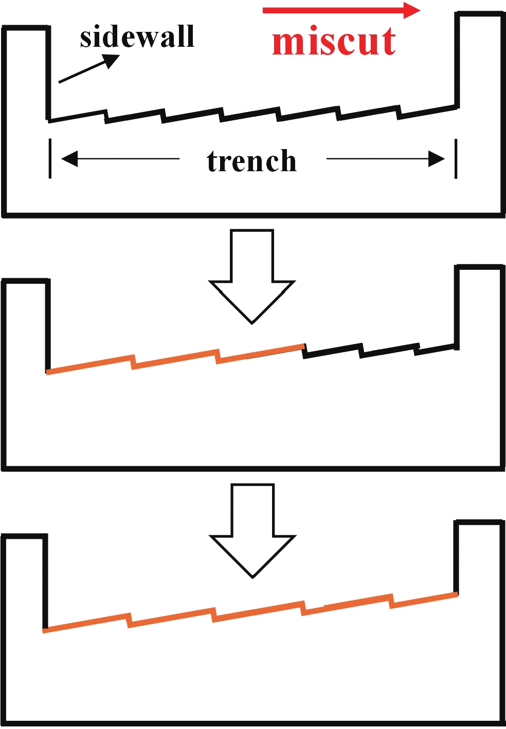
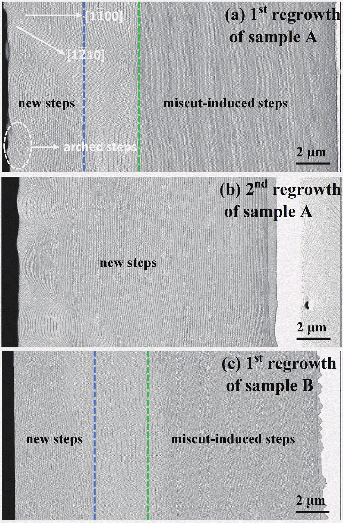
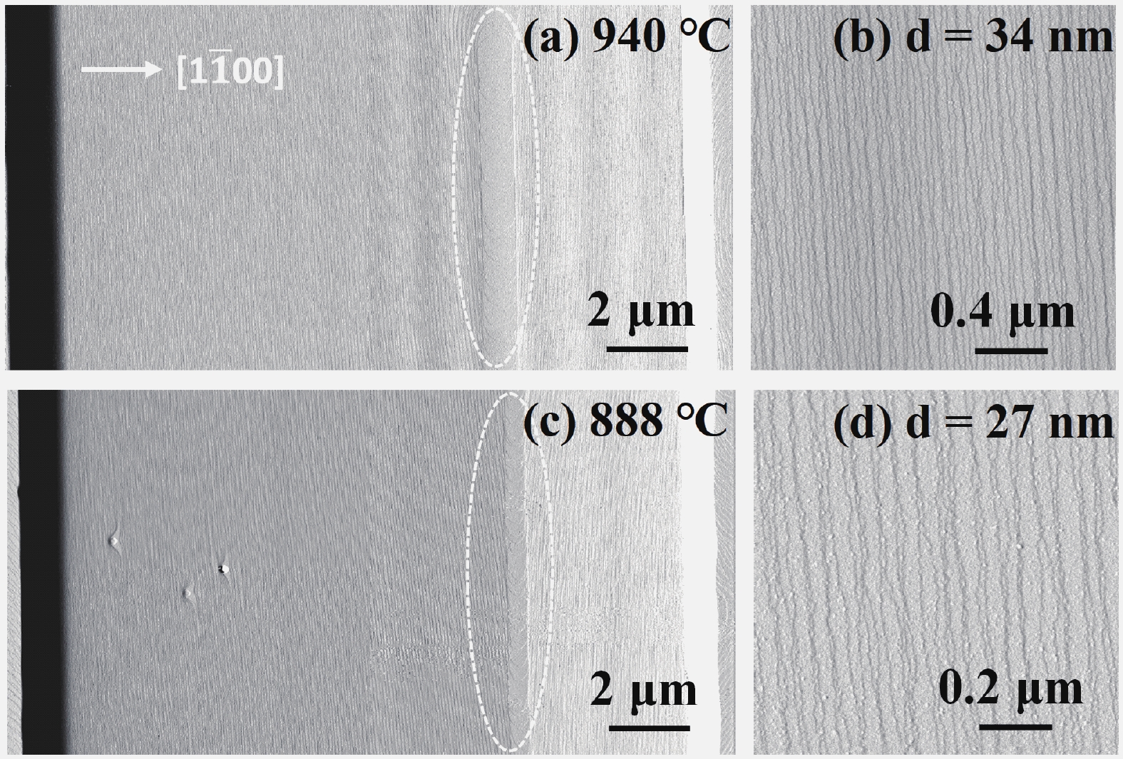
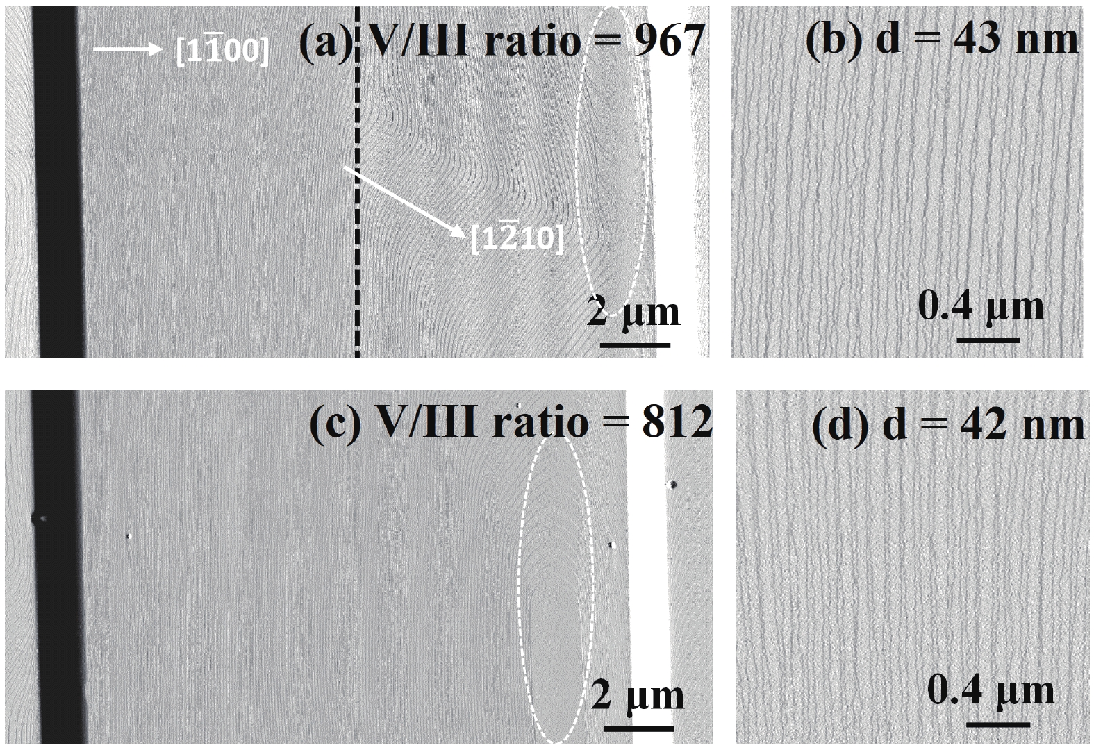
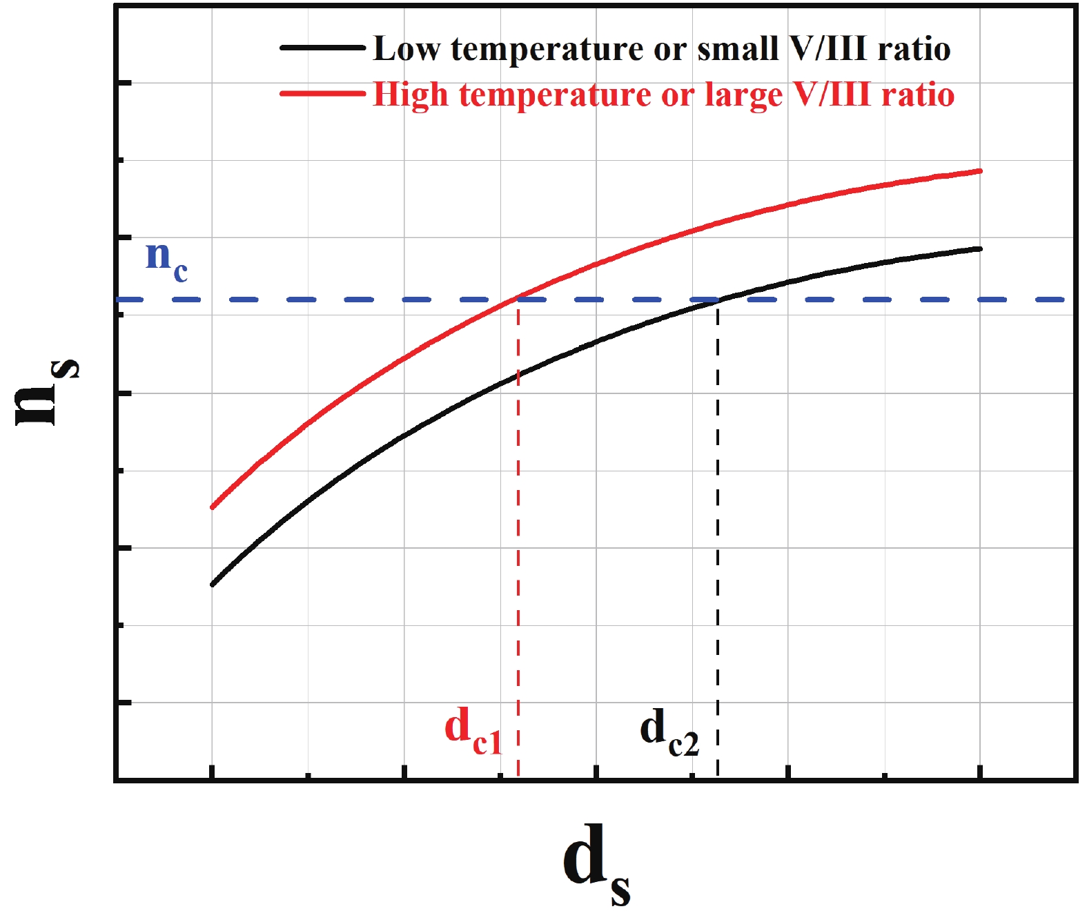
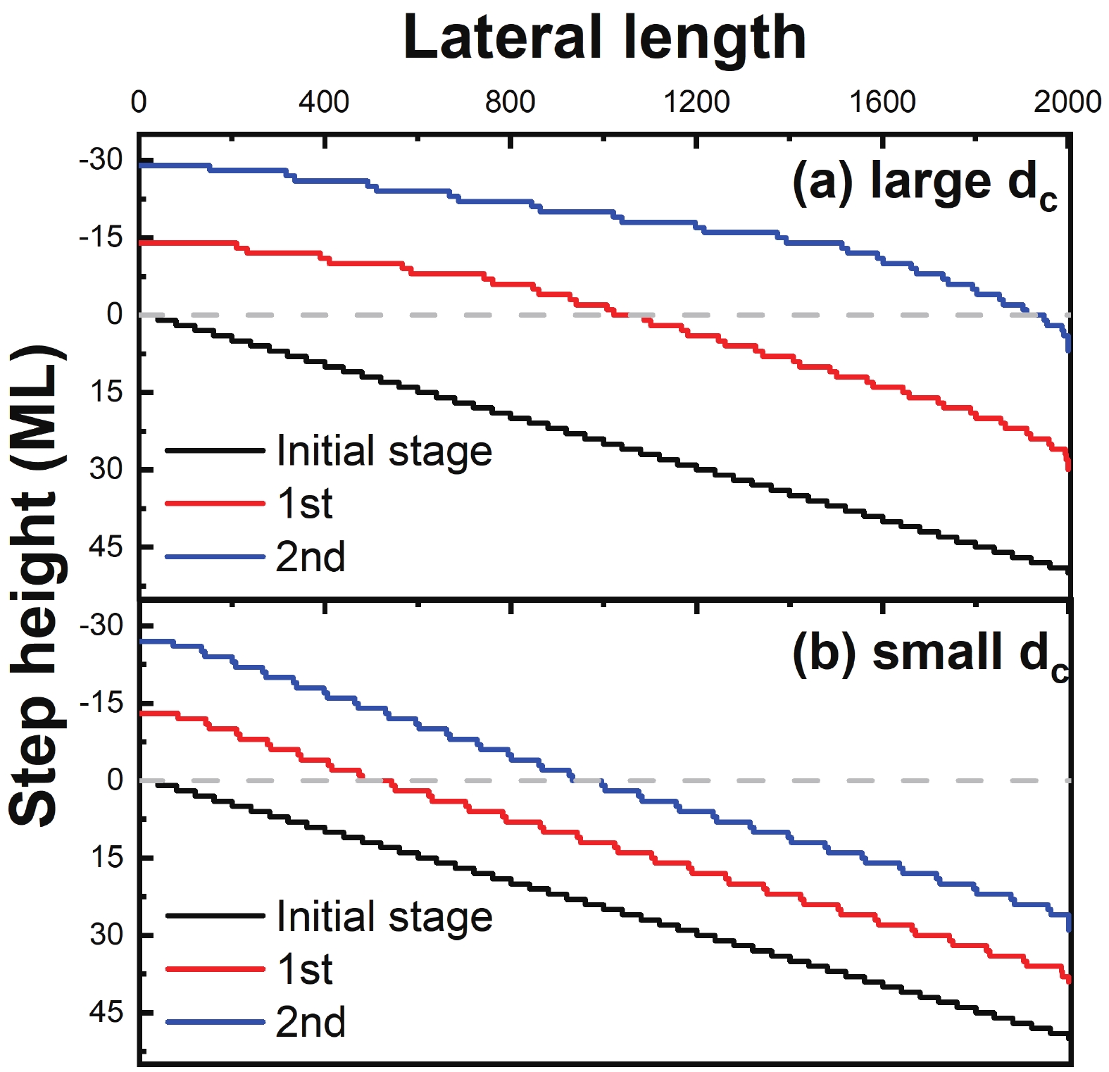
A new kind of step-flow growth mode is proposed, which adopts sidewall as step source on patterned GaN substrate. The terrace width of steps originated from the sidewall was found to change with the growth temperature and ammonia flux. The growth mechanism is explained and simulated based on step motion model. This work helps better understand the behaviors of step advancement and puts forward a method of precisely modulating atomic steps.-
Keywords:
- step-flow growth,
- GaN,
- terrace width,
- step motion
-
References
[1] Akasaka T, Gotoh H, Kobayashi Y, et al. Extremely narrow violet photoluminescence line from ultrathin InN single quantum well on step-free GaN surface. Adv Mater, 2012, 24, 4296 doi: 10.1002/adma.201200871[2] Saku T, Horikoshi Y, Tokura Y. Limit of electron mobility in AlGaAs/GaAs modulation-doped heterostructures. Jpn J Appl Phys, 1996, 35, 34 doi: 10.1143/JJAP.35.34[3] Bryan I, Bryan Z, Mita S, et al. Surface kinetics in AlN growth: A universal model for the control of surface morphology in III-nitrides. J Cryst Growth, 2016, 438, 81 doi: 10.1016/j.jcrysgro.2015.12.022[4] Jiang L R, Liu J P, Tian A Q, et al. GaN-based green laser diodes. J Semicond, 2016, 37, 111001 doi: 10.1088/1674-4926/37/11/111001[5] Shitara T, Nishinaga T. Surface diffusion length of gallium during MBE growth on the various misoriented GaAs(001) substrates. Jpn J Appl Phys, 1989, 28, 1212 doi: 10.1143/JJAP.28.1212[6] Kimoto T, Matsunami H. Surface kinetics of adatoms in vapor phase epitaxial growth of SiC on 6H-SiC{0001}vicinal surfaces. J Appl Phys, 1994, 75, 850 doi: 10.1063/1.356439[7] Mita S, Collazo R, Rice A, et al. Influence of gallium supersaturation on the properties of GaN grown by metalorganic chemical vapor deposition. J Appl Phys, 2008, 104, 13521 doi: 10.1063/1.2952027[8] Liang Y P, Liu J P, Ikeda M, et al. Effect of inhomogeneous broadening on threshold current of GaN-based green laser diodes. J Semicond, 2019, 40, 052802 doi: 10.1088/1674-4926/40/5/052802[9] Leszczynski M, Czernecki R, Krukowski S, et al. Indium incorporation into InGaN and InAlN layers grown by metalorganic vapor phase epitaxy. J Cryst Growth, 2011, 318, 496 doi: 10.1016/j.jcrysgro.2010.10.050[10] Kryśko M, Franssen G, Suski T, et al. Correlation between luminescence and compositional striations in InGaN layers grown on miscut GaN substrates. Appl Phys Lett, 2007, 91, 211904 doi: 10.1063/1.2815921[11] Uždavinys T K, Marcinkevičius S, Mensi M, et al. Impact of surface morphology on the properties of light emission in InGaN epilayers. Appl Phys Express, 2018, 11, 051004 doi: 10.7567/APEX.11.051004[12] Franssen G, Suski T, Kryśko M, et al. Influence of substrate misorientation on properties of InGaN layers grown on freestanding GaN. Phys Status Solidi (c), 2008, 5, 1485 doi: 10.1002/pssc.200778409[13] Keller S, Suh C S, Fichtenbaum N A, et al. Influence of the substrate misorientation on the properties of N-polar InGaN/GaN and AlGaN/GaN heterostructures. J Appl Phys, 2008, 104, 93510 doi: 10.1063/1.3006132[14] Bryan I, Bryan Z, Mita S, et al. The role of surface kinetics on composition and quality of AlGaN. J Cryst Growth, 2016, 451, 65 doi: 10.1016/j.jcrysgro.2016.06.055[15] Jiang L R, Liu J P, Tian A Q, et al. Influence of substrate misorientation on carbon impurity incorporation and electrical properties of p-GaN grown by metalorganic chemical vapor deposition. Appl Phys Express, 2019, 12, 055503 doi: 10.7567/1882-0786/ab0da2[16] Liu H X, Su P Y, Wu Z H, et al. Influence of substrate misorientation on the optical properties of Mg-doped GaN. J Appl Phys, 2020, 127, 195701 doi: 10.1063/5.0001482[17] Nagamatsu K, Ando Y, Kono T, et al. Effect of substrate misorientation on the concentration of impurities and surface morphology of an epitaxial GaN layer on N-polar GaN substrate by MOVPE. J Cryst Growth, 2019, 512, 78 doi: 10.1016/j.jcrysgro.2019.02.013[18] Kushimoto M, Tanikawa T, Honda Y, et al. Optically pumped lasing properties of (1-100) InGaN/GaN stripe multiquantum wells with ridge cavity structure on patterned (001) Si substrates. Appl Phys Express, 2015, 8, 022702 doi: 10.7567/APEX.8.022702[19] Zhong Y Z, Su S, Chen X, et al. Normally-off HEMTs with regrown p-GaN gate and low-pressure chemical vapor deposition SiNx passivation by using an AlN pre-layer. IEEE Electron Device Lett, 2019, 40, 1495 doi: 10.1109/LED.2019.2928027[20] Tang W X, Zhou J A, Yu G H, et al. Effects of the stepped sidewall morphology on the ON-state performance for vertical GaN trench-gate MOSFETs. Appl Phys Express, 2022, 15, 076502 doi: 10.35848/1882-0786/ac727d[21] Bales G S, Zangwill A. Morphological instability of a terrace edge during step-flow growth. Phys Rev B, 1990, 41, 5500 doi: 10.1103/PhysRevB.41.5500[22] Yoon M, Lee H N, Hong W, et al. Dynamics of step bunching in heteroepitaxial growth on vicinal substrates. Phys Rev Lett, 2007, 99, 055503 doi: 10.1103/PhysRevLett.99.055503[23] Fujikura H, Konno T. Roughening of GaN homoepitaxial surfaces due to step meandering and bunching instabilities and their suppression in hydride vapor phase epitaxy. Appl Phys Lett, 2018, 113, 152101 doi: 10.1063/1.5042572[24] Wu P, Liu J P, Jiang L R, et al. Growth behaviors of GaN on stripes of patterned c-plane GaN substrate. Nanomaterials, 2022, 12, 478 doi: 10.3390/nano12030478[25] Schwoebel R L, Shipsey E J. Step motion on crystal surfaces. J Appl Phys, 1966, 37, 3682 doi: 10.1063/1.1707904[26] Kelchner K M, Kuritzky L Y, Nakamura S, et al. Stable vicinal step orientations in m-plane GaN. J Cryst Growth, 2015, 411, 56 doi: 10.1016/j.jcrysgro.2014.10.032[27] Lin H, Li D Y, Zhang L Q, et al. Effect of microstructure of Au80Sn20 solder on the thermal resistance TO56 packaged GaN-based laser diodes. J Semicond, 2020, 41, 102104 doi: 10.1088/1674-4926/41/10/102104[28] Zhang M L, Ikeda M, Huang S Y, et al. Ni/Pd-based ohmic contacts to p-GaN through p-InGaN/p+-GaN contacting layers. J Semicond, 2022, 43, 092803 doi: 10.1088/1674-4926/43/9/092803[29] Huang S Y, Ikeda M, Zhang M L, et al. Suitable contacting scheme for evaluating electrical properties of GaN-based p-type layers. J Semicond, 2023, 44, 052802 doi: 10.1088/1674-4926/44/5/052802[30] He J L, Feng M X, Zhong Y Z, et al. On-wafer fabrication of cavity mirrors for InGaN-based laser diode grown on Si. Sci Rep, 2018, 8, 7922 doi: 10.1038/s41598-018-26305-8[31] Xie M H, Gong M, Pang E K Y, et al. Origin of triangular island shape and double-step bunching during GaN growth by molecular-beam epitaxy under excess Ga conditions. Phys Rev B, 2006, 74, 085314 doi: 10.1103/PhysRevB.74.085314[32] Zheng H, Xie M H, Wu H S, et al. Kinetic energy barriers on the GaN(0001) surface: A nucleation study by scanning tunneling microscopy. Phys Rev B, 2008, 77, 045303 doi: 10.1103/PhysRevB.77.045303[33] Miyake H, Motogaito A, Hiramatsu K. Effects of reactor pressure on epitaxial lateral overgrowth of GaN via low-pressure metalorganic vapor phase epitaxy. Jpn J Appl Phys, 1999, 38, L1000 doi: 10.1143/JJAP.38.L1000[34] Beaumont B, Vennegues P H, Gibart P. Epitaxial lateral overgrowth of GaN. Phys Stat Sol (B), 2001, 227, 1 doi: 10.1002/1521-3951(200109)227:1<1::AID-PSSB1>3.0.CO;2-Q[35] Kapolnek D, Keller S, Vetury R, et al. Anisotropic epitaxial lateral growth in GaN selective area epitaxy. Appl Phys Lett, 1997, 71, 1204 doi: 10.1063/1.119626[36] Turski H, Siekacz M, Wasilewski Z R, et al. Nonequivalent atomic step edges—role of gallium and nitrogen atoms in the growth of InGaN layers. J Cryst Growth, 2013, 367, 115 doi: 10.1016/j.jcrysgro.2012.12.026[37] Xie M H, Leung S Y, Tong S Y. What causes step bunching: Negative Ehrlich-Schwoebel barrier versus positive incorporation barrier. Surf Sci, 2002, 515, L459 doi: 10.1016/S0039-6028(02)01976-3 -
Proportional views


 Peng Wu got his bachelor’s degree in 2017 from the Yangzhou University. He is now a doctoral student at the University of Chinese Academy of Sciences under the supervision of Prof. Hui Yang and Prof. Jianping Liu. His research focuses on MOCVD growth and characterization of GaN-based materials.
 Jianping Liu is a professor at the Suzhou Institute of Nano-Tech and Nano-Bionics, CAS. He got his doctoral degree from the Institute of Semiconductors, CAS in 2004. Then he worked at the Lab of Optoelectronics Technology at Beijing University of Technology from 2004 to 2006. He did postdoctoral research in the Department of Electrical Engineering at Georgia Institute of Technology from 2006 to 2010. His research interests include MOCVD growth, GaN-based materials and devices.
 Hui Yang received his doctoral degree from the Institute of Semiconductors, CAS in 1991. Then he did postdoctoral research in the Paul-Drude-Institute for solid state electronics from 1993 to 1996. He returned to the Institute of Semiconductors to continue his research on GaN-based optoelectronic devices. Now he is a professor at the Suzhou Institute of Nano-Tech and Nano-Bionics, CAS and is interested in the growth, characterization and device fabrication of Ⅲ−Ⅴ compounds.
 DownLoad:
