


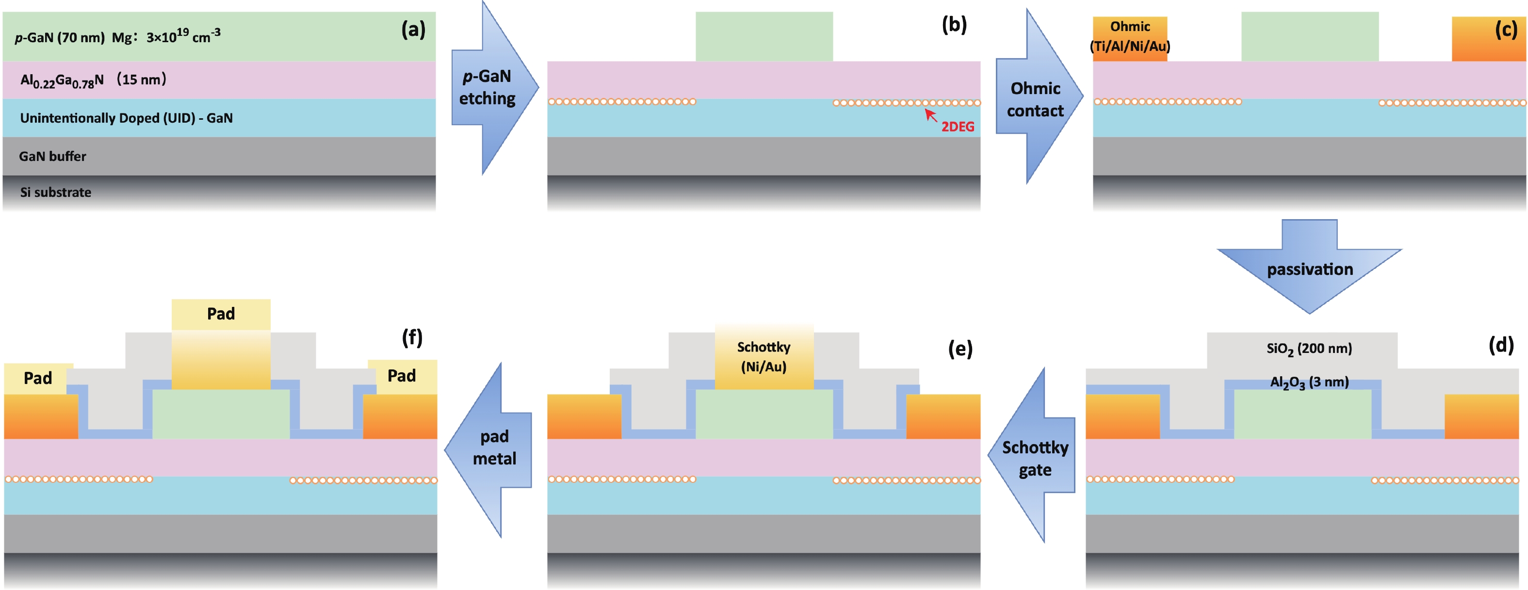
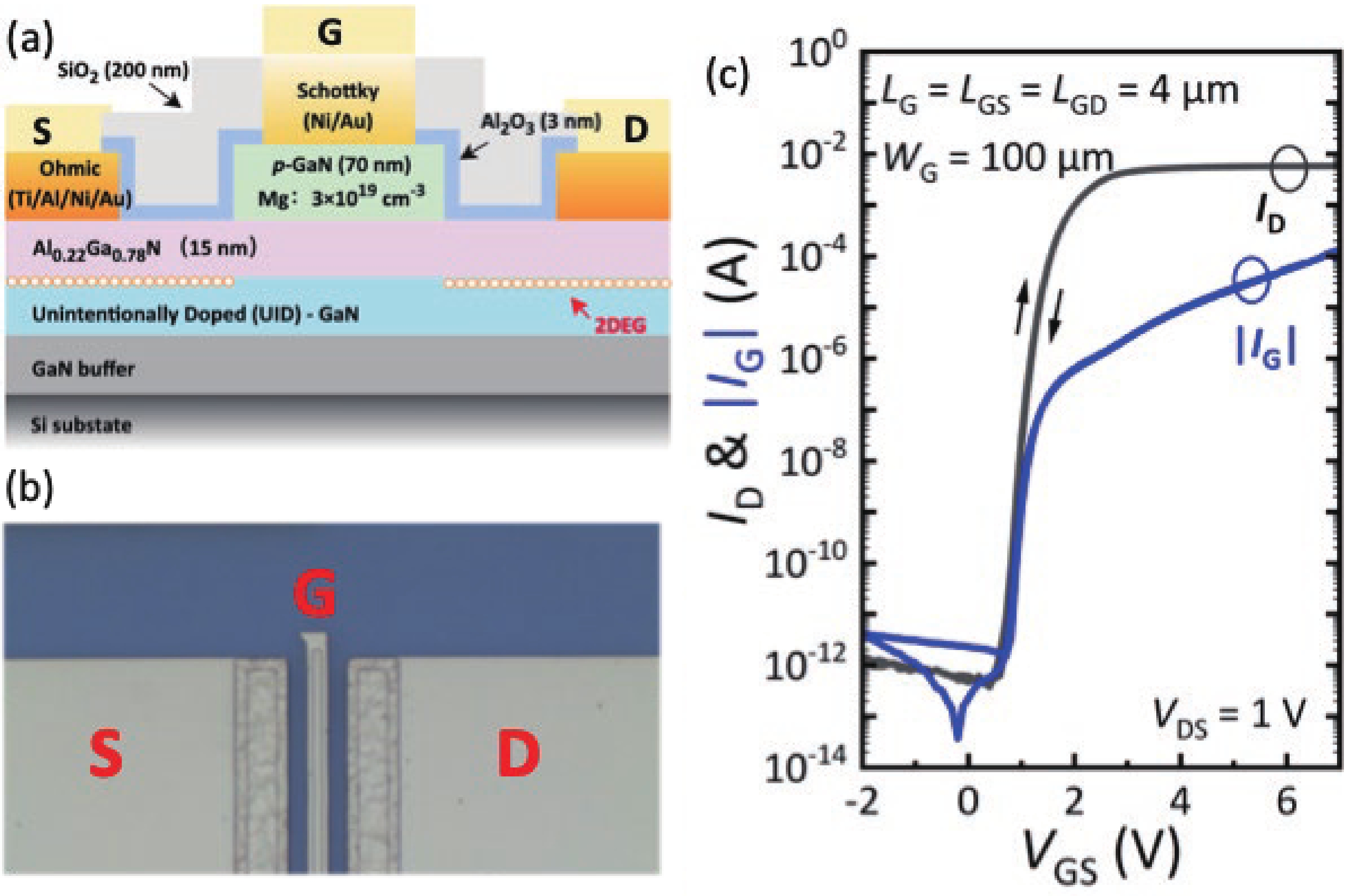
Fig. 1.
(Color online) Schematic diagram of the process flow of the Schottky-type p-GaN HEMT.
ARTICLES
Chao Feng1, 2, Xinyue Dai1, 2, Qimeng Jiang1, 2, , Sen Huang1, 2, , Jie Fan1, Xinhua Wang1, 2 and Xinyu Liu1, 2
Corresponding author: Qimeng Jiang, jiangqimeng@ime.ac.cn; Sen Huang, huangsen@ime.ac.cn
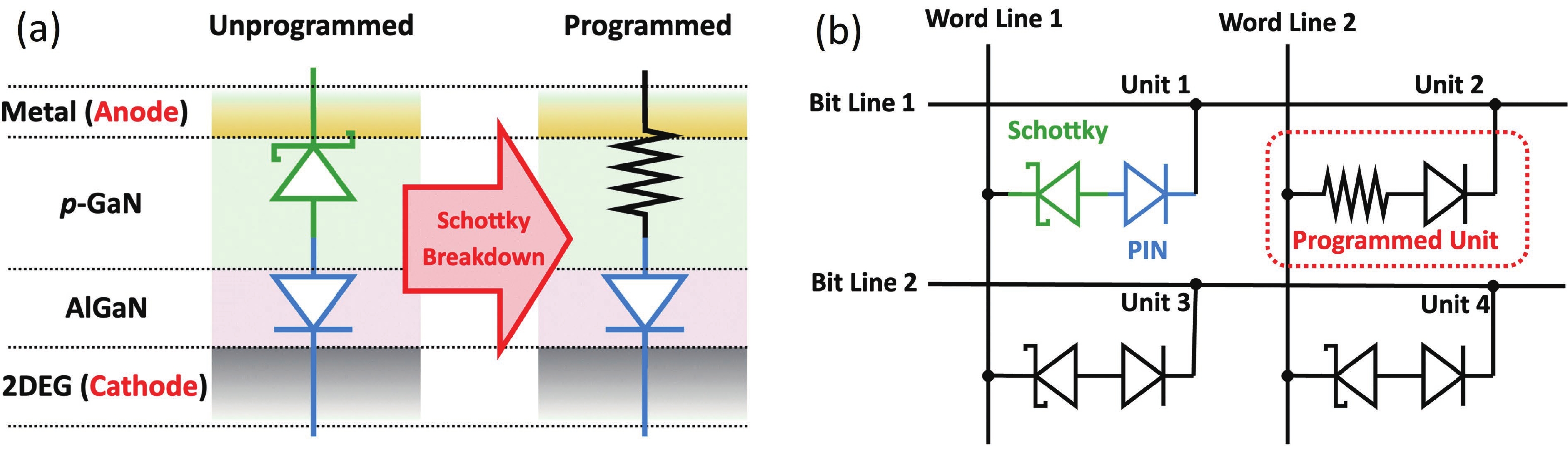
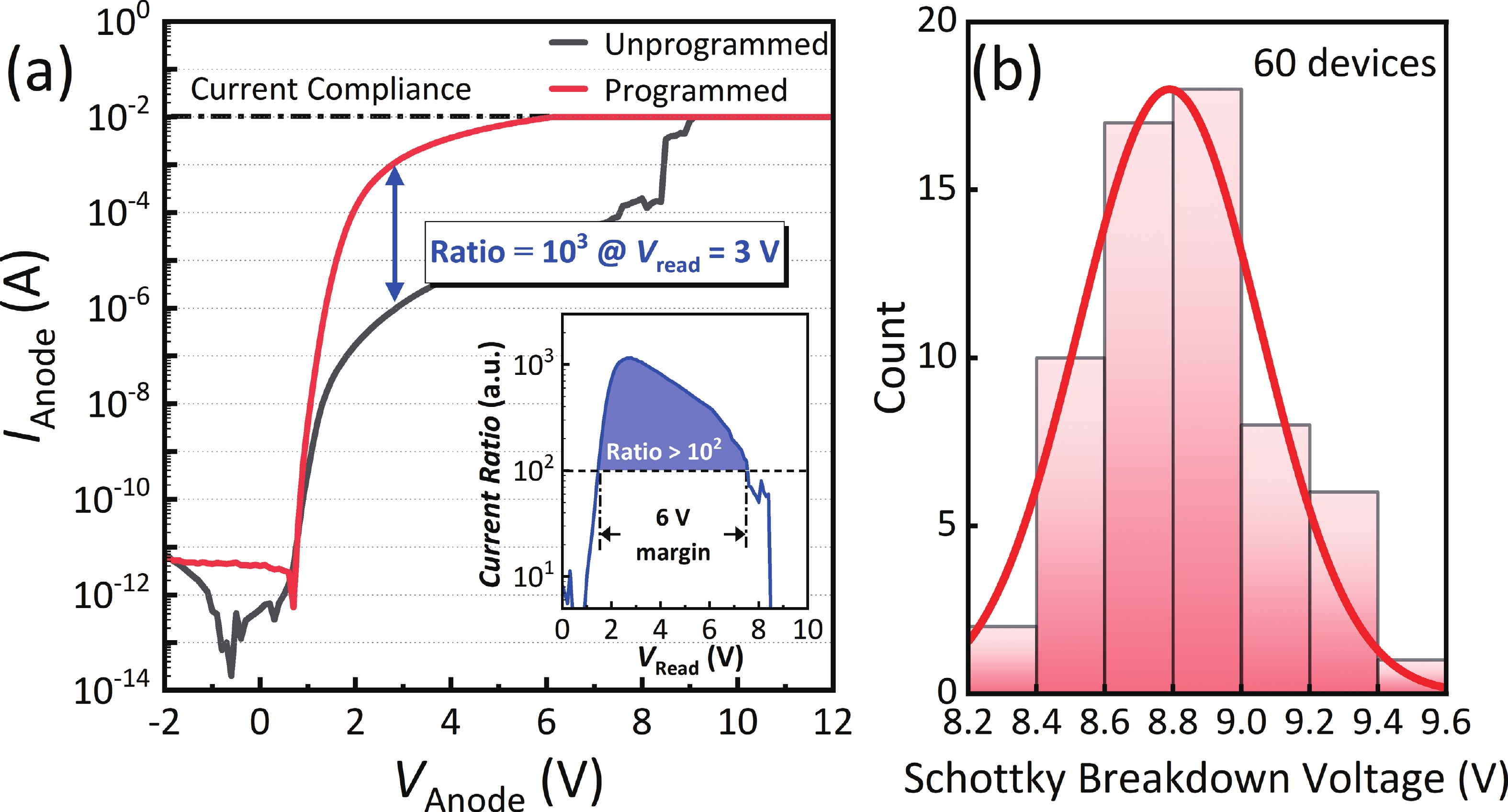
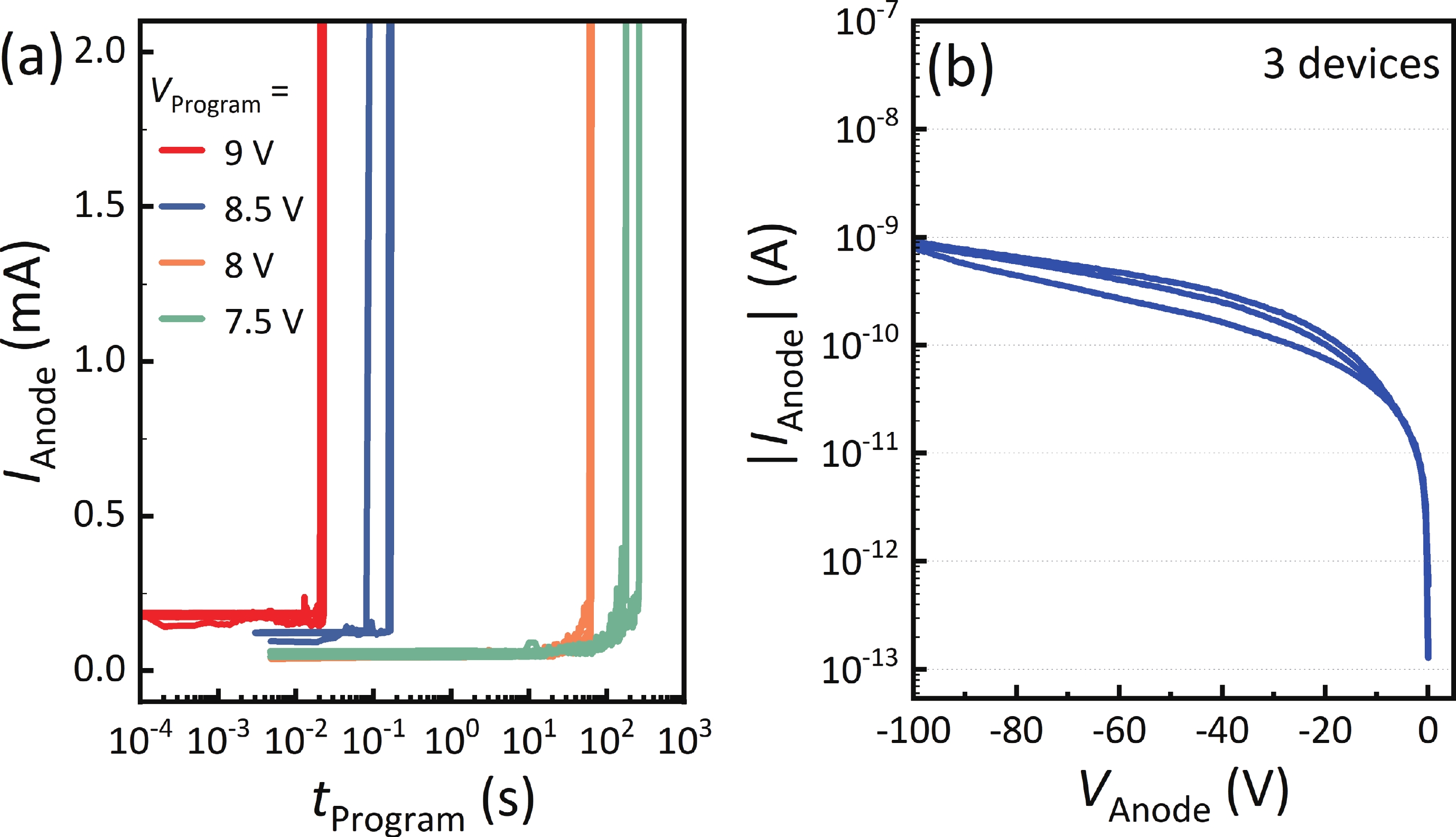
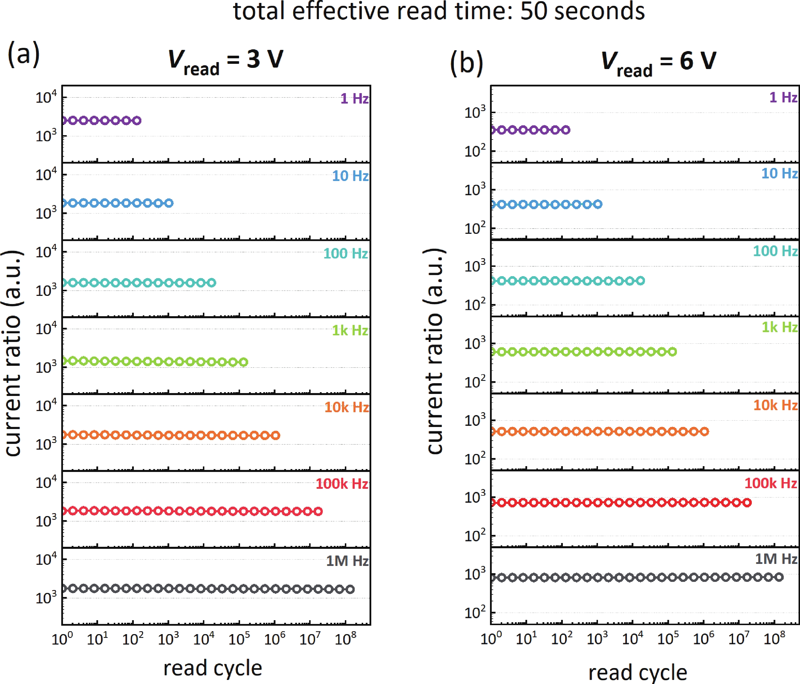
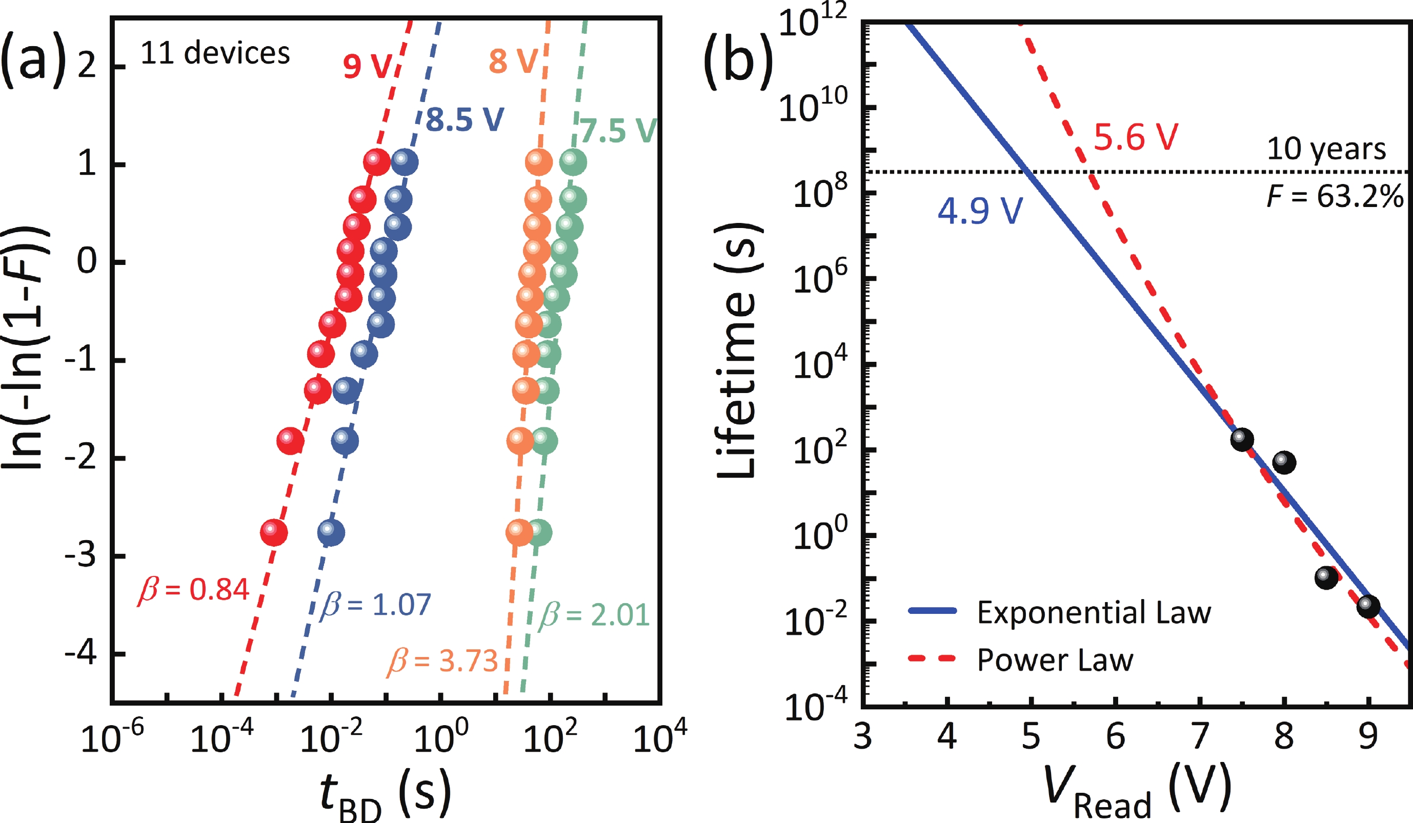
Abstract: In this work, a novel one-time-programmable memory unit based on a Schottky-type p-GaN diode is proposed. During the programming process, the junction switches from a high-resistance state to a low-resistance state through Schottky junction breakdown, and the state is permanently preserved. The memory unit features a current ratio of more than 103, a read voltage window of 6 V, a programming time of less than 10−4 s, a stability of more than 108 read cycles, and a lifetime of far more than 10 years. Besides, the fabrication of the device is fully compatible with commercial Si-based GaN process platforms, which is of great significance for the realization of low-cost read-only memory in all-GaN integration.
Keywords: wide-bandgap semiconductor, one-time programmable, Schottky-type p-GaN diode, read-only memory device
| [1] |
Chen K J, Häberlen O, Lidow A, et al. GaN-on-Si power technology: Devices and applications. IEEE Trans Electron Devices, 2017, 64, 779 doi: 10.1109/TED.2017.2657579
|
| [2] |
Amano H, Baines Y, Borga M, et al. The 2018 GaN power electronics roadmap. J Phys D: Appl Phys. 51 163001 doi: 10.1088/1361-6463/aaaf9d
|
| [3] |
Zheng Z Y, Zhang L, Song W J, et al. Gallium nitride-based complementary logic integrated circuits. Nat Electron, 2021, 4, 595 doi: 10.1038/s41928-021-00611-y
|
| [4] |
Zheng Z, Xu H, Zhang L, et al. On the operating speed and energy efficiency of GaN-based monolithic complementary logic circuits for integrated power conversion systems. Fundamental Research, 2021 , 1, 661 doi: 10.1016/j.fmre.2021.09.015
|
| [5] |
Chen Y R, Song H, Jiang H, et al. Reproducible bipolar resistive switching in entire nitride AlN/n-GaN metal-insulator-semiconductor device and its mechanism. Appl Phys Lett, 2014, 105, 193502 doi: 10.1063/1.4901747
|
| [6] |
Chen T, Zheng Z Y, Feng S R, et al. Endurance improvement of GaN bipolar charge trapping memory with back gate injection. IEEE Electron Device Lett, 2023, 44, 1408 doi: 10.1109/LED.2023.3299961
|
| [7] |
Fu K, Fu H Q, Huang X Q, et al. Threshold switching and memory behaviors of epitaxially regrown GaN-on-GaN vertical p-n diodes with high temperature stability. IEEE Electron Device Lett, 2019, 40, 375 doi: 10.1109/LED.2019.2891391
|
| [8] |
Yuan M Y, Xie Q Y, Niroula J, et al. GaN memory operational at 300 °C. IEEE Electron Device Lett, 2022, 43, 2053 doi: 10.1109/LED.2022.3218671
|
| [9] |
Sayadi L, Iannaccone G, Sicre S, et al. Threshold voltage instability in p-GaN gate AlGaN/GaN HFETs. IEEE Trans Electron Devices, 2018, 65, 2454 doi: 10.1109/TED.2018.2828702
|
| [10] |
He J, Chan W T, Wang C, et al. A compact CMOS compatible oxide antifuse with polysilicon diode driver. IEEE Trans Electron Devices, 2012, 59, 2539 doi: 10.1109/TED.2012.2201941
|
| [11] |
Kuo R J, Chang F C, King Y C, et al. Antifuse OTP cell in a cross-point array by advanced CMOS FinFET process. IEEE Trans Electron Devices, 2019, 66, 1729 doi: 10.1109/TED.2019.2900282
|
| [12] |
Ng K P, Lee M C, Kwong K C, et al. Diode based gate oxide anti-fuse one time programmable memory array in standard CMOS process. 2009 IEEE International Conference of Electron Devices and Solid-State Circuits (EDSSC), 2010, 457 doi: 10.1109/EDSSC.2009.5394219
|
| [13] |
Pushpakaran B N, Subburaj A S, Bayne S B. Commercial GaN-based power electronic systems: A review. J Electron Mater, 2020, 49, 6247 doi: 10.1007/s11664-020-08397-z
|
| [14] |
Dai X Y, Ji Z C, Jiang Q M, et al. Suppression of reverse leakage in enhancement-mode GaN high-electron-mobility transistor by extended PGaN technology. Phys Status Solidi A, 2023, 220, 2200692 doi: 10.1002/pssa.202200692
|
| [15] |
Tallarico A N, Stoffels S, Magnone P, et al. Investigation of the p-GaN gate breakdown in forward-biased GaN-based power HEMTs. IEEE Electron Device Lett, 2017, 38, 99 doi: 10.1109/LED.2016.2631640
|
| [16] |
Feng C, Jiang Q M, Huang S, et al. Gate-bias-accelerated VTH recovery on schottky-type p-GaN gate AlGaN/GaN HEMTs. IEEE Trans Electron Devices, 2023, 70, 4591 doi: 10.1109/TED.2023.3297568
|
| [17] |
Lee F, Su L Y, Wang C H, et al. Impact of gate metal on the performance of p-GaN/AlGaN/GaN high electron mobility transistors. IEEE Electron Device Lett, 2015, 36, 232 doi: 10.1109/LED.2015.2395454
|
| [18] |
Wu T L, Marcon D, You S Z, et al. Forward bias gate breakdown mechanism in enhancement-mode p-GaN gate AlGaN/GaN high-electron mobility transistors. IEEE Electron Device Lett, 2015, 36, 1001 doi: 10.1109/LED.2015.2465137
|
| [19] |
Stoffels S, Bakeroot B, Wu T L, et al. Failure mode for p-GaN gates under forward gate stress with varying Mg concentration. 2017 IEEE International Reliability Physics Symposium (IRPS), 2017, 4B doi: 10.1109/IRPS.2017.7936310
|
| [20] |
Masin F, Meneghini M, Canato E, et al. Positive temperature dependence of time-dependent breakdown of GaN-on-Si E-mode HEMTs under positive gate stress. Appl Phys Lett, 2019, 115, 052103 doi: 10.1063/1.5109301
|


Article views: 2003 Times PDF downloads: 145 Times Cited by: 0 Times
Received: 21 October 2023 Revised: 09 November 2023 Online: Accepted Manuscript: 11 December 2023Uncorrected proof: 13 December 2023Published: 15 March 2024
| Citation: |
Chao Feng, Xinyue Dai, Qimeng Jiang, Sen Huang, Jie Fan, Xinhua Wang, Xinyu Liu. A novel one-time-programmable memory unit based on Schottky-type p-GaN diode[J]. Journal of Semiconductors, 2024, 45(3): 032502. doi: 10.1088/1674-4926/45/3/032502
****
C Feng, X Y Dai, Q M Jiang, S Huang, J Fan, X H Wang, X Y Liu. A novel one-time-programmable memory unit based on Schottky-type p-GaN diode[J]. J. Semicond, 2024, 45(3): 032502. doi: 10.1088/1674-4926/45/3/032502

|
 Chao Feng received his BS degree in Materials Science and Engineering from Nanjing University of Science and Technology, Nanjing, China, in 2018. He is pursuing a PhD in microelectronics and solid-state electronics with the Institute of Microelectronics, Chinese Academy of Sciences
 Qimeng Jiang received his PhD degree from The Hong Kong University of Science and Technology, Hong Kong, China, in 2015. He is currently a professor at the Institute of Microelectronics, Chinese Academy of Sciences, Beijing. His current research interests include advanced design and fabrication technologies for power semiconductor devices and ICs
 Sen Huang received his PhD degree from Peking University, Beijing, China, in 2009. He is currently a professor at the Institute of Microelectronics, Chinese Academy of Sciences, Beijing. His current research interests include advanced design, fabrication, and characterization technologies for Ⅲ–Ⅴ power semiconductors or devices
| [1] |
Chen K J, Häberlen O, Lidow A, et al. GaN-on-Si power technology: Devices and applications. IEEE Trans Electron Devices, 2017, 64, 779 doi: 10.1109/TED.2017.2657579
|
| [2] |
Amano H, Baines Y, Borga M, et al. The 2018 GaN power electronics roadmap. J Phys D: Appl Phys. 51 163001 doi: 10.1088/1361-6463/aaaf9d
|
| [3] |
Zheng Z Y, Zhang L, Song W J, et al. Gallium nitride-based complementary logic integrated circuits. Nat Electron, 2021, 4, 595 doi: 10.1038/s41928-021-00611-y
|
| [4] |
Zheng Z, Xu H, Zhang L, et al. On the operating speed and energy efficiency of GaN-based monolithic complementary logic circuits for integrated power conversion systems. Fundamental Research, 2021 , 1, 661 doi: 10.1016/j.fmre.2021.09.015
|
| [5] |
Chen Y R, Song H, Jiang H, et al. Reproducible bipolar resistive switching in entire nitride AlN/n-GaN metal-insulator-semiconductor device and its mechanism. Appl Phys Lett, 2014, 105, 193502 doi: 10.1063/1.4901747
|
| [6] |
Chen T, Zheng Z Y, Feng S R, et al. Endurance improvement of GaN bipolar charge trapping memory with back gate injection. IEEE Electron Device Lett, 2023, 44, 1408 doi: 10.1109/LED.2023.3299961
|
| [7] |
Fu K, Fu H Q, Huang X Q, et al. Threshold switching and memory behaviors of epitaxially regrown GaN-on-GaN vertical p-n diodes with high temperature stability. IEEE Electron Device Lett, 2019, 40, 375 doi: 10.1109/LED.2019.2891391
|
| [8] |
Yuan M Y, Xie Q Y, Niroula J, et al. GaN memory operational at 300 °C. IEEE Electron Device Lett, 2022, 43, 2053 doi: 10.1109/LED.2022.3218671
|
| [9] |
Sayadi L, Iannaccone G, Sicre S, et al. Threshold voltage instability in p-GaN gate AlGaN/GaN HFETs. IEEE Trans Electron Devices, 2018, 65, 2454 doi: 10.1109/TED.2018.2828702
|
| [10] |
He J, Chan W T, Wang C, et al. A compact CMOS compatible oxide antifuse with polysilicon diode driver. IEEE Trans Electron Devices, 2012, 59, 2539 doi: 10.1109/TED.2012.2201941
|
| [11] |
Kuo R J, Chang F C, King Y C, et al. Antifuse OTP cell in a cross-point array by advanced CMOS FinFET process. IEEE Trans Electron Devices, 2019, 66, 1729 doi: 10.1109/TED.2019.2900282
|
| [12] |
Ng K P, Lee M C, Kwong K C, et al. Diode based gate oxide anti-fuse one time programmable memory array in standard CMOS process. 2009 IEEE International Conference of Electron Devices and Solid-State Circuits (EDSSC), 2010, 457 doi: 10.1109/EDSSC.2009.5394219
|
| [13] |
Pushpakaran B N, Subburaj A S, Bayne S B. Commercial GaN-based power electronic systems: A review. J Electron Mater, 2020, 49, 6247 doi: 10.1007/s11664-020-08397-z
|
| [14] |
Dai X Y, Ji Z C, Jiang Q M, et al. Suppression of reverse leakage in enhancement-mode GaN high-electron-mobility transistor by extended PGaN technology. Phys Status Solidi A, 2023, 220, 2200692 doi: 10.1002/pssa.202200692
|
| [15] |
Tallarico A N, Stoffels S, Magnone P, et al. Investigation of the p-GaN gate breakdown in forward-biased GaN-based power HEMTs. IEEE Electron Device Lett, 2017, 38, 99 doi: 10.1109/LED.2016.2631640
|
| [16] |
Feng C, Jiang Q M, Huang S, et al. Gate-bias-accelerated VTH recovery on schottky-type p-GaN gate AlGaN/GaN HEMTs. IEEE Trans Electron Devices, 2023, 70, 4591 doi: 10.1109/TED.2023.3297568
|
| [17] |
Lee F, Su L Y, Wang C H, et al. Impact of gate metal on the performance of p-GaN/AlGaN/GaN high electron mobility transistors. IEEE Electron Device Lett, 2015, 36, 232 doi: 10.1109/LED.2015.2395454
|
| [18] |
Wu T L, Marcon D, You S Z, et al. Forward bias gate breakdown mechanism in enhancement-mode p-GaN gate AlGaN/GaN high-electron mobility transistors. IEEE Electron Device Lett, 2015, 36, 1001 doi: 10.1109/LED.2015.2465137
|
| [19] |
Stoffels S, Bakeroot B, Wu T L, et al. Failure mode for p-GaN gates under forward gate stress with varying Mg concentration. 2017 IEEE International Reliability Physics Symposium (IRPS), 2017, 4B doi: 10.1109/IRPS.2017.7936310
|
| [20] |
Masin F, Meneghini M, Canato E, et al. Positive temperature dependence of time-dependent breakdown of GaN-on-Si E-mode HEMTs under positive gate stress. Appl Phys Lett, 2019, 115, 052103 doi: 10.1063/1.5109301
|

 WeChat ID
Journal of Semiconductors © 2017 All Rights Reserved 京ICP备05085259号-2

 DownLoad:

