


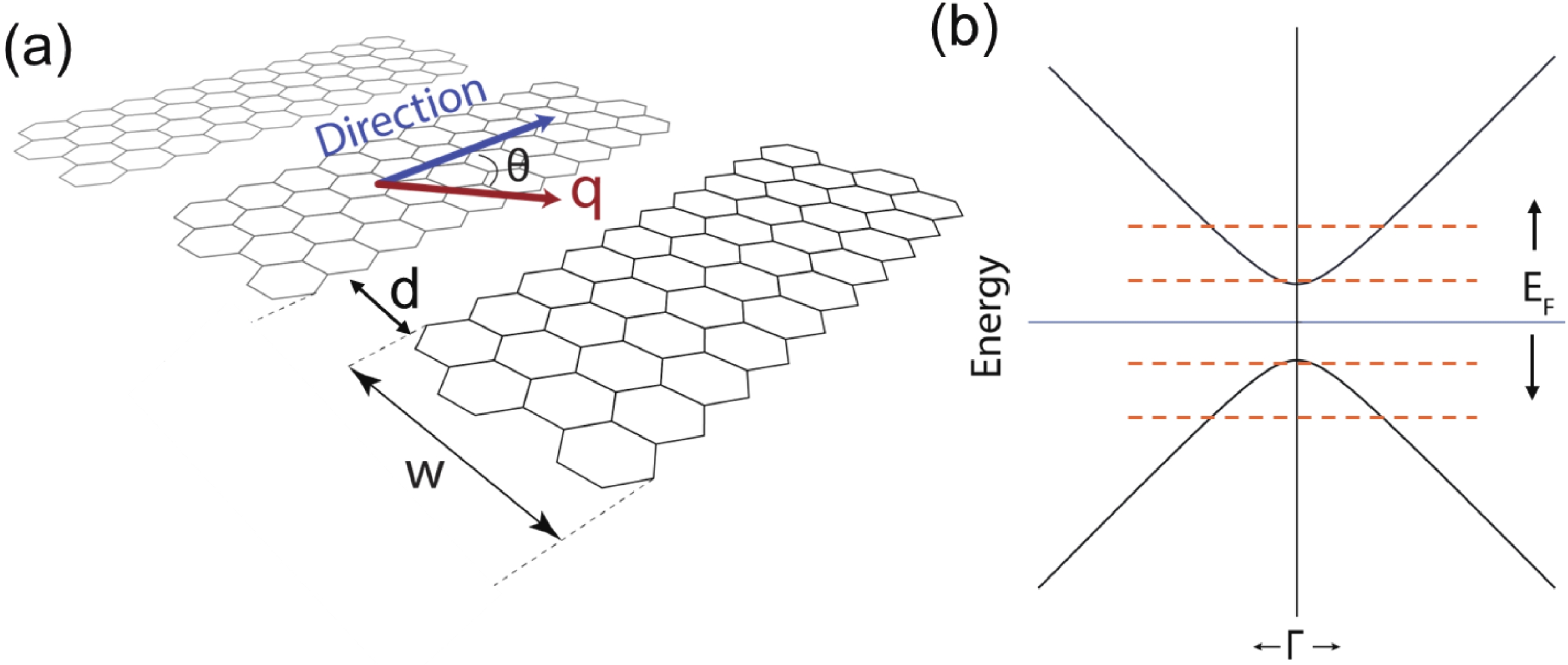
Fig. 1.
(Color online) (a) Schematic representation of GeNSs. (b) Hypothetical low-energy band structure of GeNSs, showing the modulation of charge carrier density by shifting the Fermi level (orange dashed lines).
ARTICLES
Talia Tene1, Marco Guevara2, Gabriela Tubon-Usca3, Oswaldo Villacrés Cáceres4, Gabriel Moreano5, Cristian Vacacela Gomez6, and Stefano Bellucci6,
Corresponding author: Cristian Vacacela Gomez, vacacela@lnf.infn.it; Stefano Bellucci, bellucci@lnf.infn.it
Abstract: Germanene nanostrips (GeNSs) have garnered significant attention in modern semiconductor technology due to their exceptional physical characteristics, positioning them as promising candidates for a wide range of applications. GeNSs exhibit a two-dimensional (buckled) honeycomb-like lattice, which is similar to germanene but with controllable bandgaps. The modeling of GeNSs is essential for developing appropriate synthesis methods as it enables understanding and controlling the growth process of these systems. Indeed, one can adjust the strip width, which in turn can tune the bandgap and plasmonic response of the material to meet specific device requirements. In this study, the objective is to investigate the electronic behavior and THz plasmon features of GeNSs (≥100 nm wide). A semi-analytical model based on the charge-carrier velocity of freestanding germanene is utilized for this purpose. The charge-carrier velocity of freestanding germanene is determined through the GW approximation (${v}_{\mathrm{F}}=0.702 \times {10}^{6} $ m·s−1). Within the width range of 100 to 500 nm, GeNSs exhibit narrow bandgaps, typically measuring only a few meV. Specifically, upon analysis, it was found that the bandgaps of the investigated GeNSs ranged between 29 and 6 meV. As well, these nanostrips exhibit $ \sqrt{q} $-like plasmon dispersions, with their connected plasmonic frequency (≤30 THz) capable of being manipulated by varying parameters such as strip width, excitation plasmon angle, and sample quality. These manipulations can lead to frequency variations, either increasing or decreasing, as well as shifts towards larger momentum values. The outcomes of our study serve as a foundational motivation for future experiments, and further confirmation is needed to validate the reported results.
Key words: nanostrips, carrier velocity, germanene, plasmonics, electronics
| [1] |
Sharma V, Srivastava P, Jaiswal N K. Edge-oxidized germanene nanoribbons for nanoscale metal interconnect applications. IEEE Trans Electron Devices, 2018, 65, 3893 doi: 10.1109/TED.2018.2858006
|
| [2] |
Sindona A, Vacacela Gomez C, Pisarra M. Dielectric screening versus geometry deformation in two-dimensional allotropes of silicon and germanium. Sci Rep, 2022, 12, 15107 doi: 10.1038/s41598-022-19260-y
|
| [3] |
Ouyang J, Feng C, Ji X Y, et al. 2D monoelemental germanene quantum dots: Synthesis as robust photothermal agents for photonic cancer nanomedicine. Angewandte Chemie Int Ed, 2019, 58, 13405 doi: 10.1002/anie.201908377
|
| [4] |
Gablech I, Pekárek J, Klempa J, et al. Monoelemental 2D materials-based field effect transistors for sensing and biosensing: Phosphorene, antimonene, arsenene, silicene, and germanene go beyond graphene. Trac Trends Anal Chem, 2018, 105, 251 doi: 10.1016/j.trac.2018.05.008
|
| [5] |
Ma X Y, Yang T, Li D C, et al. Elastic response of monolayer Si1– xGe x. Phys Rev B, 2022, 106, 024114 doi: 10.1103/PhysRevB.106.024114
|
| [6] |
Goldstone A, Li Q L. Band structures and electronic properties of edge-functionalized germanene nanoribbons. Appl Surf Sci, 2023, 612, 155706 doi: 10.1016/j.apsusc.2022.155706
|
| [7] |
Kharwar S, Singh S, Jaiswal N K. Giant magnetoresistance and rectification behavior in fluorinated zigzag boron nitride nanoribbon for spintronic nanodevices. IEEE Trans Nanotechnol, 2022, 21, 244 doi: 10.1109/TNANO.2022.3174247
|
| [8] |
Jung J, Bui N N, Shen S, et al. In situ surface-enhanced Raman spectroscopic studies of electrochemically formed germanene. J Phys Chem C, 2018, 122, 15696 doi: 10.1021/acs.jpcc.8b02510
|
| [9] |
Shyu F L. Magneto-plasmons of germanene nanoribbons. Phys E Low Dimensional Syst Nanostructures, 2022, 135, 114948 doi: 10.1016/j.physe.2021.114948
|
| [10] |
Kar C, Jena S, Udupa D V, et al. Tamm plasmon polariton in planar structures: A brief overview and applications. Opt Laser Technol, 2023, 159, 108928 doi: 10.1016/j.optlastec.2022.108928
|
| [11] |
Chen F Q, Yao J C, Wang X J, et al. Fast modulation of surface plasmons based on the photothermal effect of nonvolatile solid thin films. Nanoscale, 2023, 15, 476 doi: 10.1039/D2NR05527A
|
| [12] |
Repplinger T, Klimin S, Gélédan M, et al. Plasmons in three-dimensional superconductors. Phys Rev B, 2023, 107, 014504 doi: 10.1103/PhysRevB.107.014504
|
| [13] |
Fei Z, Goldflam M D, Wu J S, et al. Edge and surface plasmons in graphene nanoribbons. Nano Lett, 2015, 15, 8271 doi: 10.1021/acs.nanolett.5b03834
|
| [14] |
Vacacela Gomez C, Pisarra M, Gravina M, et al. Plasmon modes of graphene nanoribbons with periodic planar arrangements. Phys Rev Lett, 2016, 117, 116801 doi: 10.1103/PhysRevLett.117.116801
|
| [15] |
Popov V V, Bagaeva T Y, Otsuji T, et al. Oblique terahertz plasmons in graphene nanoribbon arrays. Phys Rev B, 2010, 81, 073404 doi: 10.1103/PhysRevB.81.073404
|
| [16] |
Pisarra M, Gomez C V, Sindona A. Massive and massless plasmons in germanene nanosheets. Sci Rep, 2022, 12, 18624 doi: 10.1038/s41598-022-23058-3
|
| [17] |
Bhandari A S, Verma A. A tight-binding analysis of models, sheet width, and strain for 2D monoatomic germanium sheets. Mat Express, 2019, 9, 273 doi: 10.1166/mex.2019.1488
|
| [18] |
Singh S, Garg K, Sareen A, et al. Doped armchair germanene nanoribbon exhibiting negative differential resistance and analysing its nano-FET performance. Org Electron, 2018, 54, 261 doi: 10.1016/j.orgel.2017.12.039
|
| [19] |
Tene T, Guevara M, Borja M, et al. Modeling semiconducting silicene nanostrips: Electronics and THz plasmons. Frontiers in Physics, 2023, 11, 369 doi: 10.3389/fphy.2023.1198214
|
| [20] |
Yang Y X, Murali R. Impact of size effect on graphene nanoribbon transport. IEEE Electron Device Lett, 2010, 31, 237 doi: 10.1109/LED.2009.2039915
|
| [21] |
Gonze X, Jollet F, Araujo FA, et al. Recent developments in the ABINIT software package. Comput Phys Commun, 2016, 205, 106 doi: 10.1016/j.cpc.2016.04.003
|
| [22] |
Gori-Giorgi P, Seidl M, Vignale G. Density-functional theory for strongly interacting electrons. Phys Rev Lett, 2009, 103, 166402 doi: 10.1103/PhysRevLett.103.166402
|
| [23] |
Troullier N, Martins J. A straightforward method for generating soft transferable pseudopotentials. Solid State Commun, 1990, 74, 613 doi: 10.1016/0038-1098(90)90686-6
|
| [24] |
Wisesa P, McGill K A, Mueller T. Efficient generation of generalized Monkhorst-Pack grids through the use of informatics. Phys Rev B, 2016, 93, 155109 doi: 10.1103/PhysRevB.93.155109
|
| [25] |
Aryasetiawan F, Gunnarsson O. The GW method. Rep Prog Phys, 1998, 61, 237
|
| [26] |
Hagen G, Vaagen J S, Hjorth-Jensen M. The contour deformation method in momentum space, applied to subatomic physics. J Phys A: Math Gen, 2004, 37, 8991 doi: 10.1088/0305-4470/37/38/006
|
| [27] |
Ju L, Geng B S, Horng J, et al. Graphene plasmonics for tunable terahertz metamaterials. Nat Nanotechnol, 2011, 6, 630 doi: 10.1038/nnano.2011.146
|
| [28] |
Tene T, Guevara M, Svozilík J, et al. Proving surface plasmons in graphene nanoribbons organized as 2D periodic arrays and potential applications in biosensors. Chemosensors, 2022, 10, 514 doi: 10.3390/chemosensors10120514
|
| [29] |
Wu Q L, Bagheri Tagani M, Tian Q W, et al. Symmetry breaking induced bandgap opening in epitaxial germanene on WSe2. Appl Phys Lett, 2022, 121, 051901 doi: 10.1063/5.0103367
|
| [30] |
Zhang Y B, Tan Y W, Stormer H L, et al. Experimental observation of the quantum Hall effect and Berry’s phase in graphene. Nature, 2005, 438, 201 doi: 10.1038/nature04235
|
| [31] |
Li P F, Shi R, Lin P Z, et al. First-principles calculations of plasmon excitations in graphene, silicene, and germanene. Phys Rev B, 2023, 107, 035433 doi: 10.1103/PhysRevB.107.035433
|
| [32] |
Sherman Z M, Kim K, Kang J, et al. Plasmonic response of complex nanoparticle assemblies. Nano Lett, 2023, 23, 3030 doi: 10.1021/acs.nanolett.3c00429
|
| [33] |
Zhao Z Y, Du M J, Jiang C P, et al. Terahertz inner and outer edge modes in a tetramer of strongly coupled spoof localized surface plasmons. Opt Lett, 2023, 48, 1343 doi: 10.1364/OL.483601
|
| [34] |
Egerton R F. Electron energy-loss spectroscopy in the TEM. Rep Prog Phys, 2009, 72, 016502 doi: 10.1088/0034-4885/72/1/016502
|
| [35] |
Yamaguchi J, Hayashi H, Jippo H, et al. Small bandgap in atomically precise 17-atom-wide armchair-edged graphene nanoribbons. Commun Mater, 2020, 1, 36 doi: 10.1038/s43246-020-0039-9
|
| [36] |
Liou F, Tsai H Z, Aikawa A S, et al. Imaging reconfigurable molecular concentration on a graphene field-effect transistor. Nano Lett, 2021, 21, 8770 doi: 10.1021/acs.nanolett.1c03039
|
| [37] |
Shen C, Ledwith P J, Watanabe K, et al. Dirac spectroscopy of strongly correlated phases in twisted trilayer graphene. Nat Mater, 2023, 22, 316 doi: 10.1038/s41563-022-01428-6
|
| [38] |
Han M Y, Ozyilmaz B, Zhang Y B, et al. Energy band-gap engineering of graphene nanoribbons. Phys Rev Lett, 2007, 98, 206805 doi: 10.1103/PhysRevLett.98.206805
|
| [39] |
Yang L, Park C H, Son Y W, et al. Quasiparticle energies and band gaps in graphene nanoribbons. Phys Rev Lett, 2007, 99, 186801 doi: 10.1103/PhysRevLett.99.186801
|
| [40] |
Xu Y, Yan B H, Zhang H J, et al. Large-gap quantum spin hall insulators in tin films. Phys Rev Lett, 2013, 111, 136804 doi: 10.1103/PhysRevLett.111.136804
|
| [41] |
Acun A, Zhang L, Bampoulis P, et al. Germanene: The germanium analogue of graphene. J Phys Condens Matter, 2015, 27, 443002 doi: 10.1088/0953-8984/27/44/443002
|
| [42] |
Kiraly B, Mannix A J, Jacobberger R M, et al. Sub-5 nm, globally aligned graphene nanoribbons on Ge(001). Appl Phys Lett, 2016, 108, 213101 doi: 10.1063/1.4950959
|

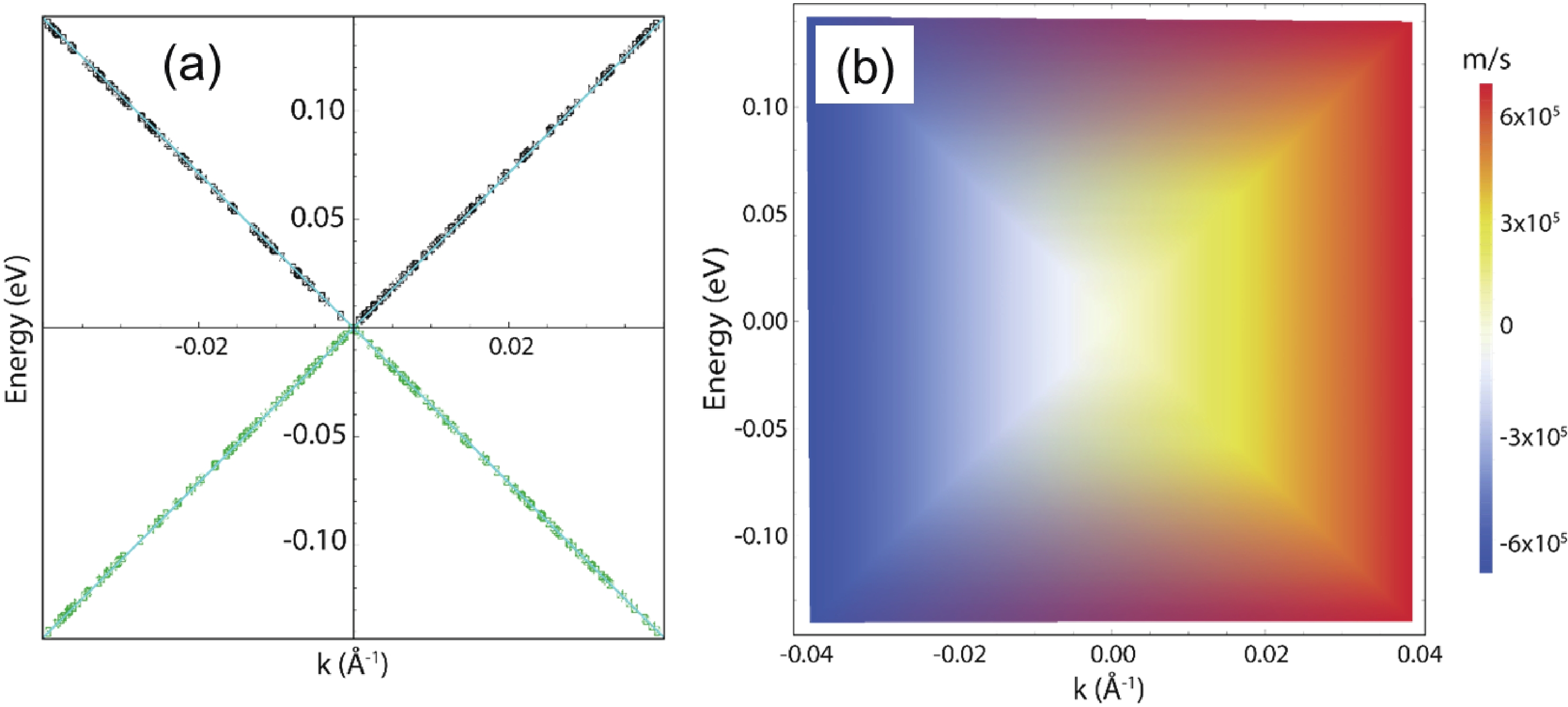
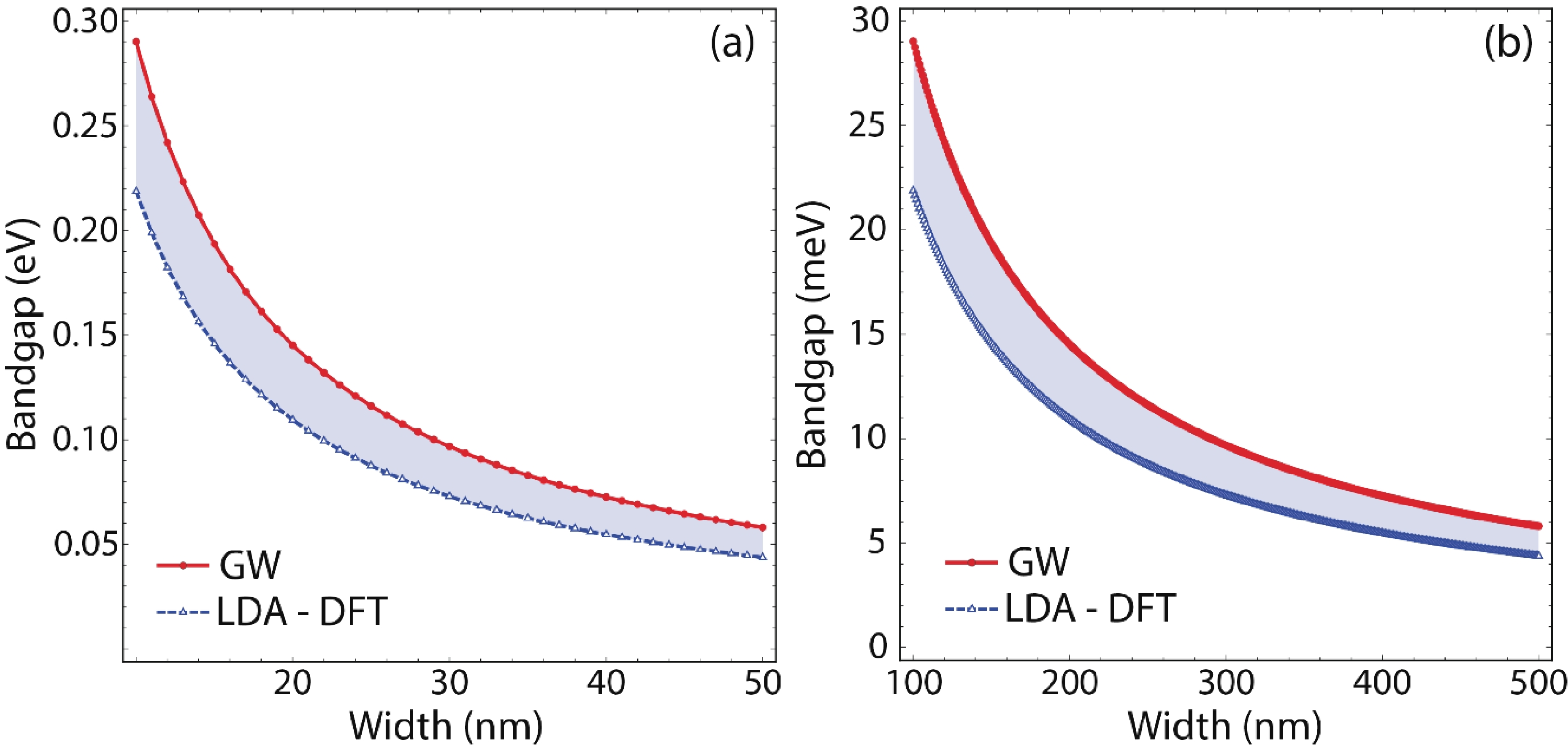
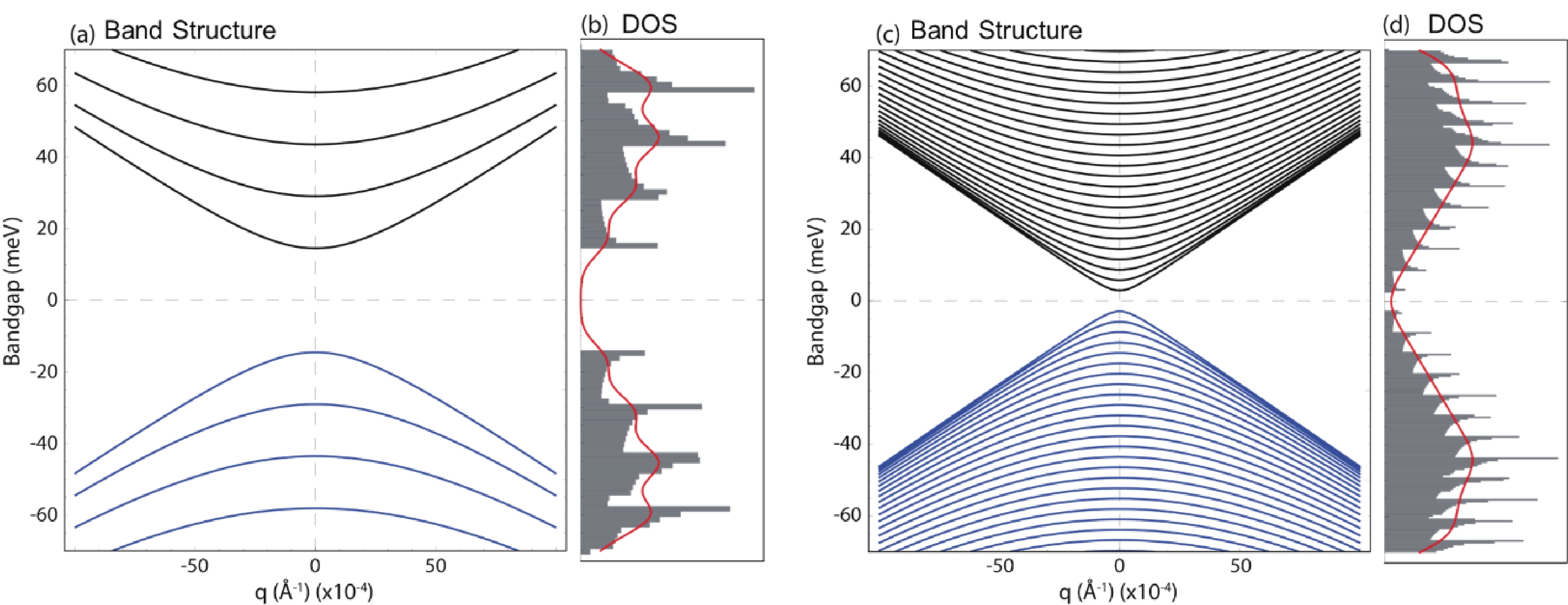
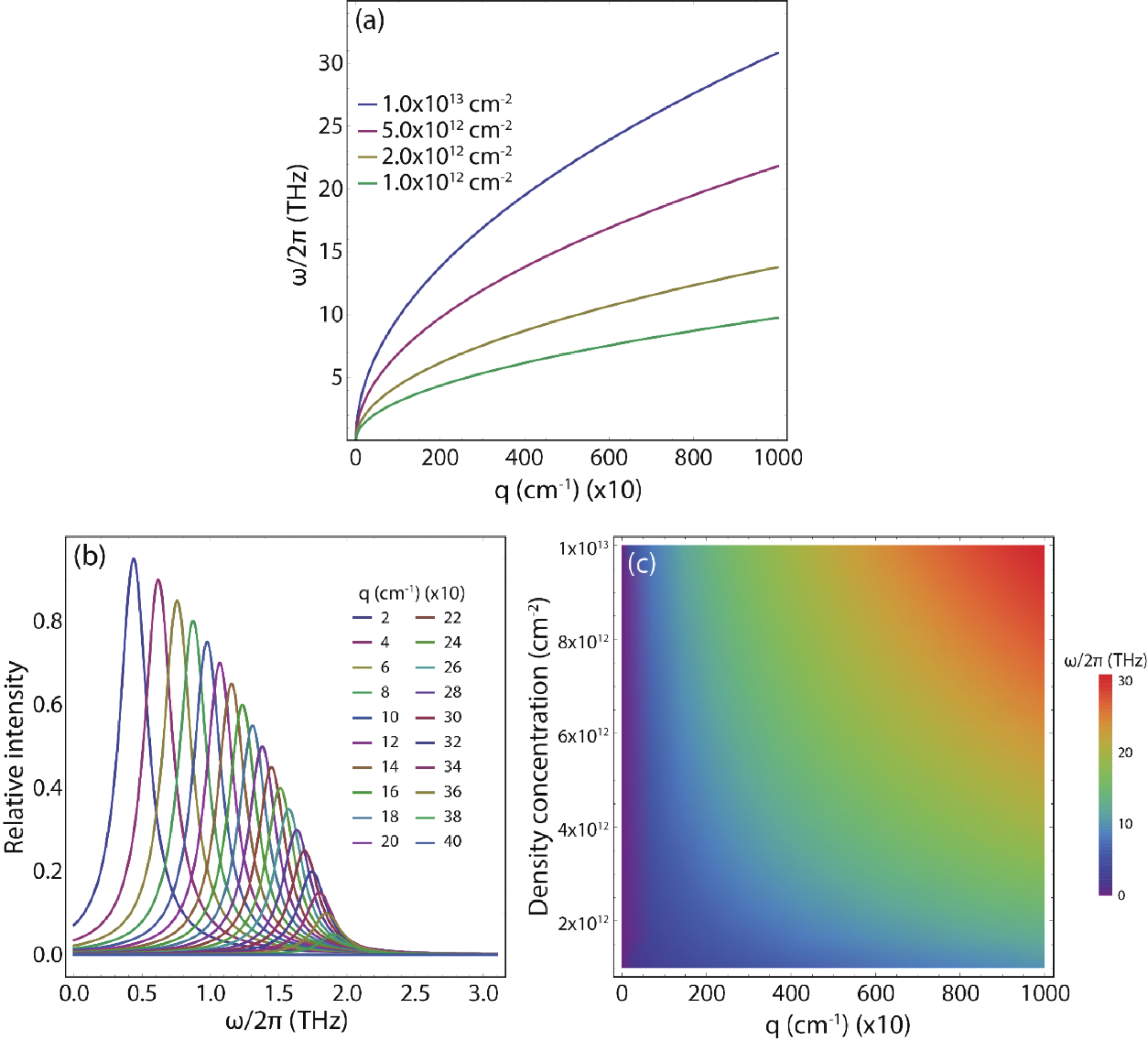
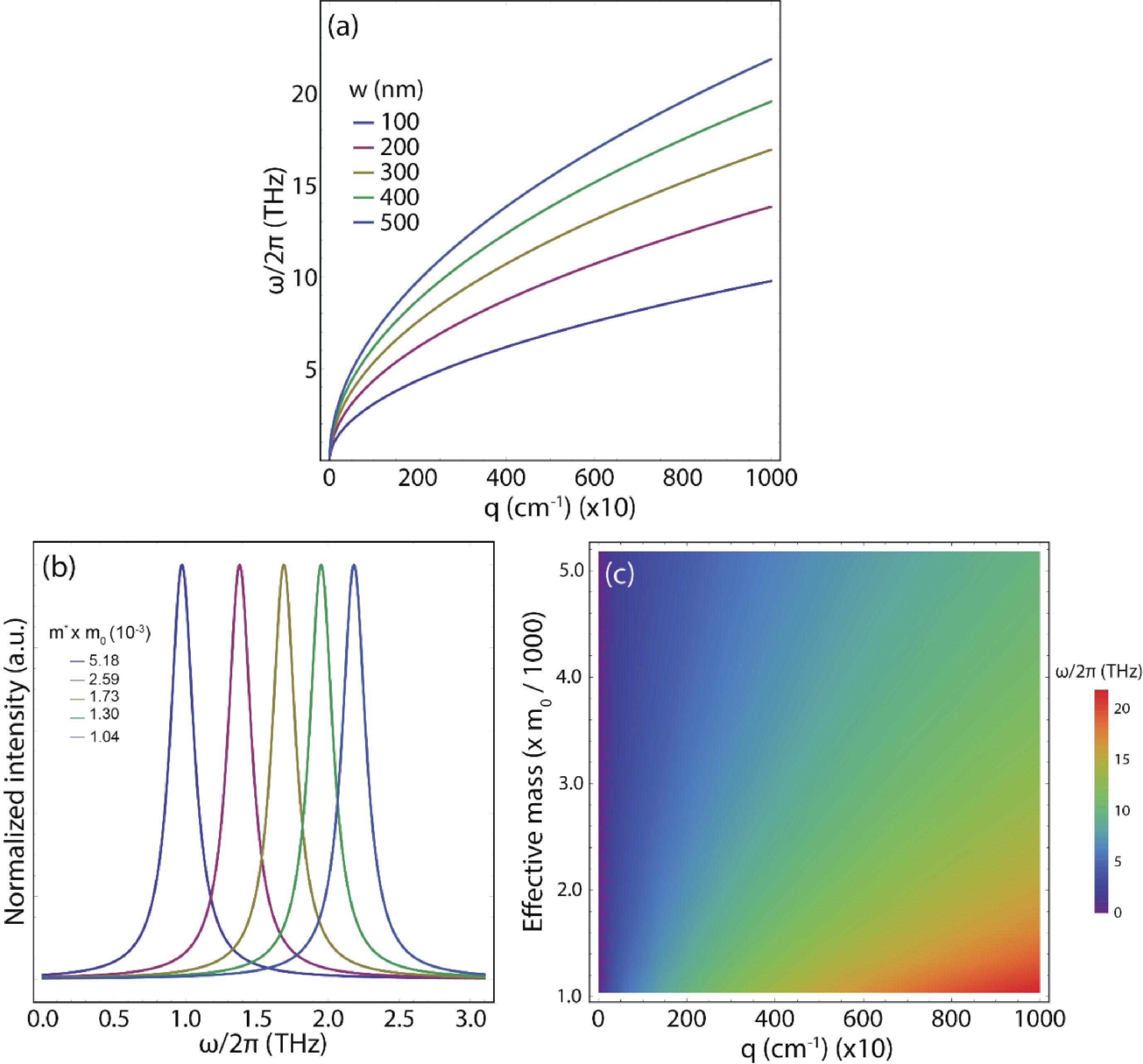
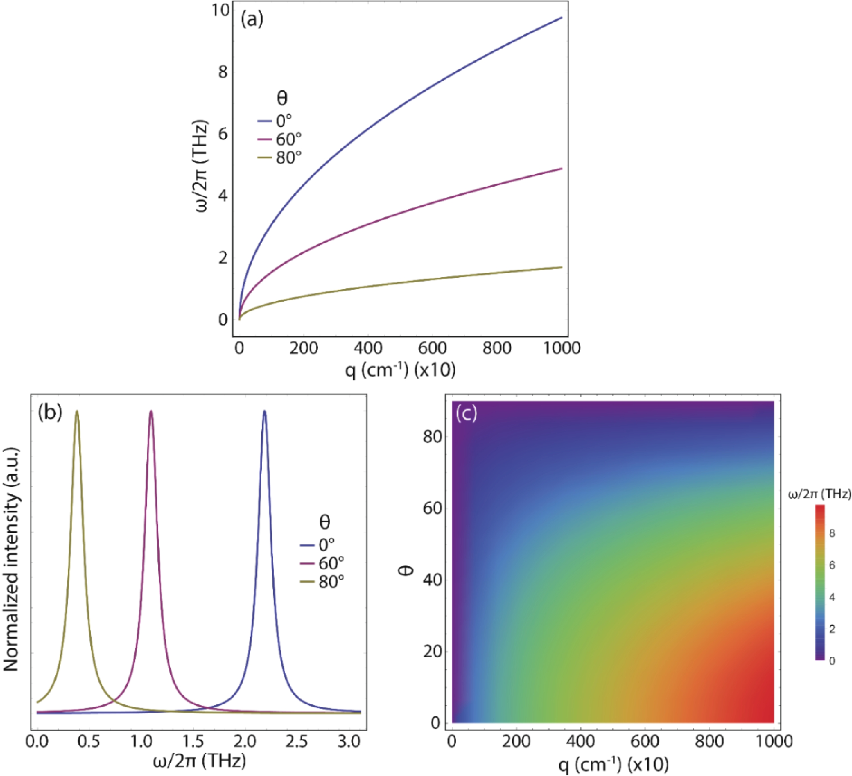
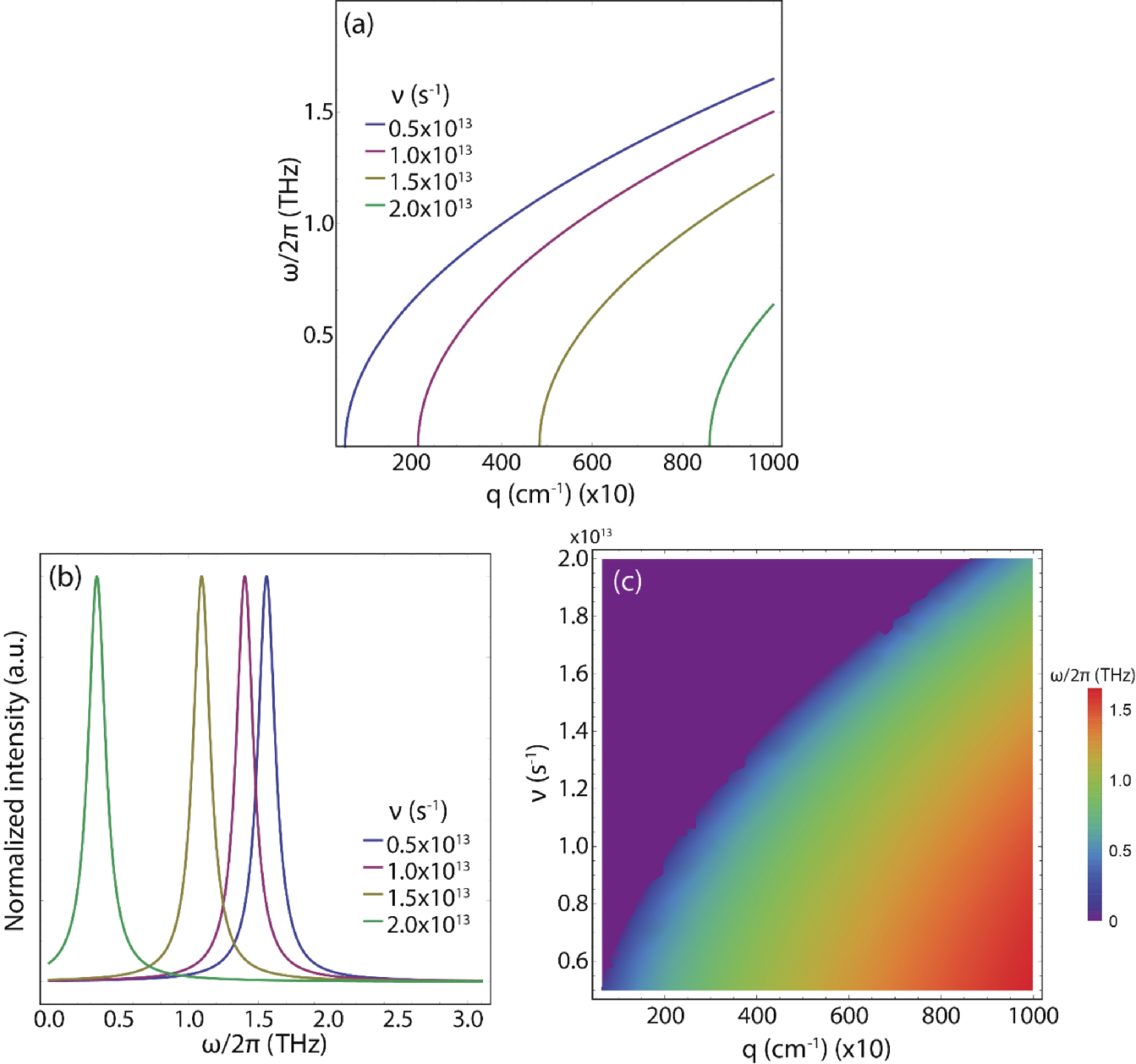
Table 1. The estimated group velocity of suspended germanene and graphene by GW and DFT calculations compared with the available experimental value.
| Method | Value (106 m·s−1) | Variation percentage (%) |
| LDA-DFT | 0.527 | −24.93 |
| GW | 0.702 | −37.21 |
| GW-gr | 1.118 | +1.64 |
| Exp-gr | 1.1 | − |
 DownLoad: CSV
Table 2. Bandgap values and effective electron masses of chosen GeNSs (see Fig. 3(b)). It is pointed out that $ {m}_{0} $ denotes the free electron mass.
| Strip width (nm) | $ \mathrm{\Delta } $ (meV) | $ {{m}}^{{*}}\times {{m}}_{0} $ (10−3) |
| 100 | 29.03 | 5.18 |
| 200 | 14.52 | 2.59 |
| 300 | 9.68 | 1.73 |
| 400 | 7.26 | 1.30 |
| 500 | 5.81 | 1.04 |
DownLoad: CSV
Table 3. Variation of carrier density and Fermi level by adjusting the distance between GeNSs.
| $ {d} $ (nm) | $ {{N}}_{2\mathbf{D}} $ (cm−2) | $ {{E}}_{\mathbf{F}} $ (eV) |
| 10 | $ 1\times {10}^{13} $ | 0.37 |
| 20 | $ 5\times {10}^{12} $ | 0.26 |
| 50 | $ 2\times {10}^{12} $ | 0.16 |
| 100 | $ 1\times {10}^{12} $ | 0.12 |
DownLoad: CSV
Table 4. Estimated values of electron relaxation rate ($ \nu $), plasmon relaxation rate ($ \gamma $), and electron mobility ($ \upsilon $).
| $ {\nu } $ (1013 s−1) | $ {\gamma } $ (1012 s−1) | $ {e} $ mobility (cm2/(V∙s)) |
| 0.5 | 2.5 | 57705 |
| 1.0 | 5.0 | 48677 |
| 1.5 | 7.5 | 39650 |
| 2.0 | 10 | 30622 |
DownLoad: CSV
| [1] |
Sharma V, Srivastava P, Jaiswal N K. Edge-oxidized germanene nanoribbons for nanoscale metal interconnect applications. IEEE Trans Electron Devices, 2018, 65, 3893 doi: 10.1109/TED.2018.2858006
|
| [2] |
Sindona A, Vacacela Gomez C, Pisarra M. Dielectric screening versus geometry deformation in two-dimensional allotropes of silicon and germanium. Sci Rep, 2022, 12, 15107 doi: 10.1038/s41598-022-19260-y
|
| [3] |
Ouyang J, Feng C, Ji X Y, et al. 2D monoelemental germanene quantum dots: Synthesis as robust photothermal agents for photonic cancer nanomedicine. Angewandte Chemie Int Ed, 2019, 58, 13405 doi: 10.1002/anie.201908377
|
| [4] |
Gablech I, Pekárek J, Klempa J, et al. Monoelemental 2D materials-based field effect transistors for sensing and biosensing: Phosphorene, antimonene, arsenene, silicene, and germanene go beyond graphene. Trac Trends Anal Chem, 2018, 105, 251 doi: 10.1016/j.trac.2018.05.008
|
| [5] |
Ma X Y, Yang T, Li D C, et al. Elastic response of monolayer Si1– xGe x. Phys Rev B, 2022, 106, 024114 doi: 10.1103/PhysRevB.106.024114
|
| [6] |
Goldstone A, Li Q L. Band structures and electronic properties of edge-functionalized germanene nanoribbons. Appl Surf Sci, 2023, 612, 155706 doi: 10.1016/j.apsusc.2022.155706
|
| [7] |
Kharwar S, Singh S, Jaiswal N K. Giant magnetoresistance and rectification behavior in fluorinated zigzag boron nitride nanoribbon for spintronic nanodevices. IEEE Trans Nanotechnol, 2022, 21, 244 doi: 10.1109/TNANO.2022.3174247
|
| [8] |
Jung J, Bui N N, Shen S, et al. In situ surface-enhanced Raman spectroscopic studies of electrochemically formed germanene. J Phys Chem C, 2018, 122, 15696 doi: 10.1021/acs.jpcc.8b02510
|
| [9] |
Shyu F L. Magneto-plasmons of germanene nanoribbons. Phys E Low Dimensional Syst Nanostructures, 2022, 135, 114948 doi: 10.1016/j.physe.2021.114948
|
| [10] |
Kar C, Jena S, Udupa D V, et al. Tamm plasmon polariton in planar structures: A brief overview and applications. Opt Laser Technol, 2023, 159, 108928 doi: 10.1016/j.optlastec.2022.108928
|
| [11] |
Chen F Q, Yao J C, Wang X J, et al. Fast modulation of surface plasmons based on the photothermal effect of nonvolatile solid thin films. Nanoscale, 2023, 15, 476 doi: 10.1039/D2NR05527A
|
| [12] |
Repplinger T, Klimin S, Gélédan M, et al. Plasmons in three-dimensional superconductors. Phys Rev B, 2023, 107, 014504 doi: 10.1103/PhysRevB.107.014504
|
| [13] |
Fei Z, Goldflam M D, Wu J S, et al. Edge and surface plasmons in graphene nanoribbons. Nano Lett, 2015, 15, 8271 doi: 10.1021/acs.nanolett.5b03834
|
| [14] |
Vacacela Gomez C, Pisarra M, Gravina M, et al. Plasmon modes of graphene nanoribbons with periodic planar arrangements. Phys Rev Lett, 2016, 117, 116801 doi: 10.1103/PhysRevLett.117.116801
|
| [15] |
Popov V V, Bagaeva T Y, Otsuji T, et al. Oblique terahertz plasmons in graphene nanoribbon arrays. Phys Rev B, 2010, 81, 073404 doi: 10.1103/PhysRevB.81.073404
|
| [16] |
Pisarra M, Gomez C V, Sindona A. Massive and massless plasmons in germanene nanosheets. Sci Rep, 2022, 12, 18624 doi: 10.1038/s41598-022-23058-3
|
| [17] |
Bhandari A S, Verma A. A tight-binding analysis of models, sheet width, and strain for 2D monoatomic germanium sheets. Mat Express, 2019, 9, 273 doi: 10.1166/mex.2019.1488
|
| [18] |
Singh S, Garg K, Sareen A, et al. Doped armchair germanene nanoribbon exhibiting negative differential resistance and analysing its nano-FET performance. Org Electron, 2018, 54, 261 doi: 10.1016/j.orgel.2017.12.039
|
| [19] |
Tene T, Guevara M, Borja M, et al. Modeling semiconducting silicene nanostrips: Electronics and THz plasmons. Frontiers in Physics, 2023, 11, 369 doi: 10.3389/fphy.2023.1198214
|
| [20] |
Yang Y X, Murali R. Impact of size effect on graphene nanoribbon transport. IEEE Electron Device Lett, 2010, 31, 237 doi: 10.1109/LED.2009.2039915
|
| [21] |
Gonze X, Jollet F, Araujo FA, et al. Recent developments in the ABINIT software package. Comput Phys Commun, 2016, 205, 106 doi: 10.1016/j.cpc.2016.04.003
|
| [22] |
Gori-Giorgi P, Seidl M, Vignale G. Density-functional theory for strongly interacting electrons. Phys Rev Lett, 2009, 103, 166402 doi: 10.1103/PhysRevLett.103.166402
|
| [23] |
Troullier N, Martins J. A straightforward method for generating soft transferable pseudopotentials. Solid State Commun, 1990, 74, 613 doi: 10.1016/0038-1098(90)90686-6
|
| [24] |
Wisesa P, McGill K A, Mueller T. Efficient generation of generalized Monkhorst-Pack grids through the use of informatics. Phys Rev B, 2016, 93, 155109 doi: 10.1103/PhysRevB.93.155109
|
| [25] |
Aryasetiawan F, Gunnarsson O. The GW method. Rep Prog Phys, 1998, 61, 237
|
| [26] |
Hagen G, Vaagen J S, Hjorth-Jensen M. The contour deformation method in momentum space, applied to subatomic physics. J Phys A: Math Gen, 2004, 37, 8991 doi: 10.1088/0305-4470/37/38/006
|
| [27] |
Ju L, Geng B S, Horng J, et al. Graphene plasmonics for tunable terahertz metamaterials. Nat Nanotechnol, 2011, 6, 630 doi: 10.1038/nnano.2011.146
|
| [28] |
Tene T, Guevara M, Svozilík J, et al. Proving surface plasmons in graphene nanoribbons organized as 2D periodic arrays and potential applications in biosensors. Chemosensors, 2022, 10, 514 doi: 10.3390/chemosensors10120514
|
| [29] |
Wu Q L, Bagheri Tagani M, Tian Q W, et al. Symmetry breaking induced bandgap opening in epitaxial germanene on WSe2. Appl Phys Lett, 2022, 121, 051901 doi: 10.1063/5.0103367
|
| [30] |
Zhang Y B, Tan Y W, Stormer H L, et al. Experimental observation of the quantum Hall effect and Berry’s phase in graphene. Nature, 2005, 438, 201 doi: 10.1038/nature04235
|
| [31] |
Li P F, Shi R, Lin P Z, et al. First-principles calculations of plasmon excitations in graphene, silicene, and germanene. Phys Rev B, 2023, 107, 035433 doi: 10.1103/PhysRevB.107.035433
|
| [32] |
Sherman Z M, Kim K, Kang J, et al. Plasmonic response of complex nanoparticle assemblies. Nano Lett, 2023, 23, 3030 doi: 10.1021/acs.nanolett.3c00429
|
| [33] |
Zhao Z Y, Du M J, Jiang C P, et al. Terahertz inner and outer edge modes in a tetramer of strongly coupled spoof localized surface plasmons. Opt Lett, 2023, 48, 1343 doi: 10.1364/OL.483601
|
| [34] |
Egerton R F. Electron energy-loss spectroscopy in the TEM. Rep Prog Phys, 2009, 72, 016502 doi: 10.1088/0034-4885/72/1/016502
|
| [35] |
Yamaguchi J, Hayashi H, Jippo H, et al. Small bandgap in atomically precise 17-atom-wide armchair-edged graphene nanoribbons. Commun Mater, 2020, 1, 36 doi: 10.1038/s43246-020-0039-9
|
| [36] |
Liou F, Tsai H Z, Aikawa A S, et al. Imaging reconfigurable molecular concentration on a graphene field-effect transistor. Nano Lett, 2021, 21, 8770 doi: 10.1021/acs.nanolett.1c03039
|
| [37] |
Shen C, Ledwith P J, Watanabe K, et al. Dirac spectroscopy of strongly correlated phases in twisted trilayer graphene. Nat Mater, 2023, 22, 316 doi: 10.1038/s41563-022-01428-6
|
| [38] |
Han M Y, Ozyilmaz B, Zhang Y B, et al. Energy band-gap engineering of graphene nanoribbons. Phys Rev Lett, 2007, 98, 206805 doi: 10.1103/PhysRevLett.98.206805
|
| [39] |
Yang L, Park C H, Son Y W, et al. Quasiparticle energies and band gaps in graphene nanoribbons. Phys Rev Lett, 2007, 99, 186801 doi: 10.1103/PhysRevLett.99.186801
|
| [40] |
Xu Y, Yan B H, Zhang H J, et al. Large-gap quantum spin hall insulators in tin films. Phys Rev Lett, 2013, 111, 136804 doi: 10.1103/PhysRevLett.111.136804
|
| [41] |
Acun A, Zhang L, Bampoulis P, et al. Germanene: The germanium analogue of graphene. J Phys Condens Matter, 2015, 27, 443002 doi: 10.1088/0953-8984/27/44/443002
|
| [42] |
Kiraly B, Mannix A J, Jacobberger R M, et al. Sub-5 nm, globally aligned graphene nanoribbons on Ge(001). Appl Phys Lett, 2016, 108, 213101 doi: 10.1063/1.4950959
|


Article views: 714 Times PDF downloads: 64 Times Cited by: 0 Times
Received: 24 March 2023 Revised: 27 May 2023 Online: Uncorrected proof: 24 August 2023Published: 10 October 2023
| Citation: |
Talia Tene, Marco Guevara, Gabriela Tubon-Usca, Oswaldo Villacrés Cáceres, Gabriel Moreano, Cristian Vacacela Gomez, Stefano Bellucci. THz plasmonics and electronics in germanene nanostrips[J]. Journal of Semiconductors, 2023, 44(10): 102001. doi: 10.1088/1674-4926/44/10/102001
****
T Tene, M Guevara, G Tubon-Usca, O Villacrés Cáceres, G Moreano, C Vacacela Gomez, S Bellucci. THz plasmonics and electronics in germanene nanostrips[J]. J. Semicond, 2023, 44(10): 102001. doi: 10.1088/1674-4926/44/10/102001

|
 Talia Tene:holds a doctoral degree in Physics and Quantum Technologies from the University of Calabria, Italy, in 2017. She obtained, in 2013, a Bachelor's degree in Biophysics from Escuela Superior Politécnica de Chimborazo. She is currently an associate professor at Chemical Department at Universidad Técnica Particular de Loja, Ecuador. Her research focuses on the design of experiments and data analysis in the synthesis of novel materials, with particular emphasis on their electronic and optical applications. She is additionally interested in the use of ionizing radiation and its monitoring
 Gabriela Tubon-Usca:received her bachelor’s degree in Electronics and Computing for the Escuela Superior Politécnica de Chimborazo in 2010 and her doctoral degree from the University of Calabria, Italy, in 2016. Currently, she is an assistant professor at Escuela Superior Politécnica de Chimborazo, she is working in the Advanced Materials Research Group (GIMA) and Chemical Engineering department. Her interest in research includes 2D nanomaterials and organic nanomaterials, focusing on electronic devices and sensor applications
 Oswaldo Villacrés Cáceres:holds a bachelor's degree in Informatics Systems Engineering from the Escuela Superior Politécnica de Chimborazo, Ecuador, obtained in 2011. He also earned a master's degree in Database Management from the Technical University of Ambato, Ecuador, in 2016. Currently, he is a Lecturer in the Faculty of Science at Escuela Superior Politécnica de Chimborazo. His research interests revolve around algorithms and databases
 Cristian Vacacela Gomez:holds a Bachelor's degree in Biophysics from the Escuela Superior Politécnica de Chimborazo (Ecuador), obtained in 2013, and a Ph.D. in Physics and Quantum Technologies from the University of Calabria (Italy), obtained in 2017. He has also served as a visiting researcher at INTEMA (Instituto de Investigaciones en Ciencia y Tecnología de Materiales) in Argentina (2012). Currently, Cristian works as a postdoctoral fellow at the Laboratori Nazionali di Frascati - Istituto Nazionale di Fisica Nucleare (LNF - INFN), focusing on the synthesis, characterization, and modeling of nanoscale materials
 Stefano Bellucci:obtained, in 1982, a Bachelor's degree in physics from the University Sapienza Rome and, in 1986, a Ph.D. in the physics of elementary particles at SISSA, Trieste. He was a research associate at Brandeis University, Waltham, MA, USA (1983–1985); as well as a visiting researcher at M.I.T., Cambridge, MA, USA (1985–1986); the University of Maryland, USA (1986–1987); and the University of California at Davis, USA (1987–1988). He became a tenured researcher (research staff) at the INFN (Istituto Nazionale di Fisica Nucleare) Laboratori Nazionali di Frascati (LNF) in 1987, and he has been an INFN first researcher (senior research staff) since 2005
| [1] |
Sharma V, Srivastava P, Jaiswal N K. Edge-oxidized germanene nanoribbons for nanoscale metal interconnect applications. IEEE Trans Electron Devices, 2018, 65, 3893 doi: 10.1109/TED.2018.2858006
|
| [2] |
Sindona A, Vacacela Gomez C, Pisarra M. Dielectric screening versus geometry deformation in two-dimensional allotropes of silicon and germanium. Sci Rep, 2022, 12, 15107 doi: 10.1038/s41598-022-19260-y
|
| [3] |
Ouyang J, Feng C, Ji X Y, et al. 2D monoelemental germanene quantum dots: Synthesis as robust photothermal agents for photonic cancer nanomedicine. Angewandte Chemie Int Ed, 2019, 58, 13405 doi: 10.1002/anie.201908377
|
| [4] |
Gablech I, Pekárek J, Klempa J, et al. Monoelemental 2D materials-based field effect transistors for sensing and biosensing: Phosphorene, antimonene, arsenene, silicene, and germanene go beyond graphene. Trac Trends Anal Chem, 2018, 105, 251 doi: 10.1016/j.trac.2018.05.008
|
| [5] |
Ma X Y, Yang T, Li D C, et al. Elastic response of monolayer Si1– xGe x. Phys Rev B, 2022, 106, 024114 doi: 10.1103/PhysRevB.106.024114
|
| [6] |
Goldstone A, Li Q L. Band structures and electronic properties of edge-functionalized germanene nanoribbons. Appl Surf Sci, 2023, 612, 155706 doi: 10.1016/j.apsusc.2022.155706
|
| [7] |
Kharwar S, Singh S, Jaiswal N K. Giant magnetoresistance and rectification behavior in fluorinated zigzag boron nitride nanoribbon for spintronic nanodevices. IEEE Trans Nanotechnol, 2022, 21, 244 doi: 10.1109/TNANO.2022.3174247
|
| [8] |
Jung J, Bui N N, Shen S, et al. In situ surface-enhanced Raman spectroscopic studies of electrochemically formed germanene. J Phys Chem C, 2018, 122, 15696 doi: 10.1021/acs.jpcc.8b02510
|
| [9] |
Shyu F L. Magneto-plasmons of germanene nanoribbons. Phys E Low Dimensional Syst Nanostructures, 2022, 135, 114948 doi: 10.1016/j.physe.2021.114948
|
| [10] |
Kar C, Jena S, Udupa D V, et al. Tamm plasmon polariton in planar structures: A brief overview and applications. Opt Laser Technol, 2023, 159, 108928 doi: 10.1016/j.optlastec.2022.108928
|
| [11] |
Chen F Q, Yao J C, Wang X J, et al. Fast modulation of surface plasmons based on the photothermal effect of nonvolatile solid thin films. Nanoscale, 2023, 15, 476 doi: 10.1039/D2NR05527A
|
| [12] |
Repplinger T, Klimin S, Gélédan M, et al. Plasmons in three-dimensional superconductors. Phys Rev B, 2023, 107, 014504 doi: 10.1103/PhysRevB.107.014504
|
| [13] |
Fei Z, Goldflam M D, Wu J S, et al. Edge and surface plasmons in graphene nanoribbons. Nano Lett, 2015, 15, 8271 doi: 10.1021/acs.nanolett.5b03834
|
| [14] |
Vacacela Gomez C, Pisarra M, Gravina M, et al. Plasmon modes of graphene nanoribbons with periodic planar arrangements. Phys Rev Lett, 2016, 117, 116801 doi: 10.1103/PhysRevLett.117.116801
|
| [15] |
Popov V V, Bagaeva T Y, Otsuji T, et al. Oblique terahertz plasmons in graphene nanoribbon arrays. Phys Rev B, 2010, 81, 073404 doi: 10.1103/PhysRevB.81.073404
|
| [16] |
Pisarra M, Gomez C V, Sindona A. Massive and massless plasmons in germanene nanosheets. Sci Rep, 2022, 12, 18624 doi: 10.1038/s41598-022-23058-3
|
| [17] |
Bhandari A S, Verma A. A tight-binding analysis of models, sheet width, and strain for 2D monoatomic germanium sheets. Mat Express, 2019, 9, 273 doi: 10.1166/mex.2019.1488
|
| [18] |
Singh S, Garg K, Sareen A, et al. Doped armchair germanene nanoribbon exhibiting negative differential resistance and analysing its nano-FET performance. Org Electron, 2018, 54, 261 doi: 10.1016/j.orgel.2017.12.039
|
| [19] |
Tene T, Guevara M, Borja M, et al. Modeling semiconducting silicene nanostrips: Electronics and THz plasmons. Frontiers in Physics, 2023, 11, 369 doi: 10.3389/fphy.2023.1198214
|
| [20] |
Yang Y X, Murali R. Impact of size effect on graphene nanoribbon transport. IEEE Electron Device Lett, 2010, 31, 237 doi: 10.1109/LED.2009.2039915
|
| [21] |
Gonze X, Jollet F, Araujo FA, et al. Recent developments in the ABINIT software package. Comput Phys Commun, 2016, 205, 106 doi: 10.1016/j.cpc.2016.04.003
|
| [22] |
Gori-Giorgi P, Seidl M, Vignale G. Density-functional theory for strongly interacting electrons. Phys Rev Lett, 2009, 103, 166402 doi: 10.1103/PhysRevLett.103.166402
|
| [23] |
Troullier N, Martins J. A straightforward method for generating soft transferable pseudopotentials. Solid State Commun, 1990, 74, 613 doi: 10.1016/0038-1098(90)90686-6
|
| [24] |
Wisesa P, McGill K A, Mueller T. Efficient generation of generalized Monkhorst-Pack grids through the use of informatics. Phys Rev B, 2016, 93, 155109 doi: 10.1103/PhysRevB.93.155109
|
| [25] |
Aryasetiawan F, Gunnarsson O. The GW method. Rep Prog Phys, 1998, 61, 237
|
| [26] |
Hagen G, Vaagen J S, Hjorth-Jensen M. The contour deformation method in momentum space, applied to subatomic physics. J Phys A: Math Gen, 2004, 37, 8991 doi: 10.1088/0305-4470/37/38/006
|
| [27] |
Ju L, Geng B S, Horng J, et al. Graphene plasmonics for tunable terahertz metamaterials. Nat Nanotechnol, 2011, 6, 630 doi: 10.1038/nnano.2011.146
|
| [28] |
Tene T, Guevara M, Svozilík J, et al. Proving surface plasmons in graphene nanoribbons organized as 2D periodic arrays and potential applications in biosensors. Chemosensors, 2022, 10, 514 doi: 10.3390/chemosensors10120514
|
| [29] |
Wu Q L, Bagheri Tagani M, Tian Q W, et al. Symmetry breaking induced bandgap opening in epitaxial germanene on WSe2. Appl Phys Lett, 2022, 121, 051901 doi: 10.1063/5.0103367
|
| [30] |
Zhang Y B, Tan Y W, Stormer H L, et al. Experimental observation of the quantum Hall effect and Berry’s phase in graphene. Nature, 2005, 438, 201 doi: 10.1038/nature04235
|
| [31] |
Li P F, Shi R, Lin P Z, et al. First-principles calculations of plasmon excitations in graphene, silicene, and germanene. Phys Rev B, 2023, 107, 035433 doi: 10.1103/PhysRevB.107.035433
|
| [32] |
Sherman Z M, Kim K, Kang J, et al. Plasmonic response of complex nanoparticle assemblies. Nano Lett, 2023, 23, 3030 doi: 10.1021/acs.nanolett.3c00429
|
| [33] |
Zhao Z Y, Du M J, Jiang C P, et al. Terahertz inner and outer edge modes in a tetramer of strongly coupled spoof localized surface plasmons. Opt Lett, 2023, 48, 1343 doi: 10.1364/OL.483601
|
| [34] |
Egerton R F. Electron energy-loss spectroscopy in the TEM. Rep Prog Phys, 2009, 72, 016502 doi: 10.1088/0034-4885/72/1/016502
|
| [35] |
Yamaguchi J, Hayashi H, Jippo H, et al. Small bandgap in atomically precise 17-atom-wide armchair-edged graphene nanoribbons. Commun Mater, 2020, 1, 36 doi: 10.1038/s43246-020-0039-9
|
| [36] |
Liou F, Tsai H Z, Aikawa A S, et al. Imaging reconfigurable molecular concentration on a graphene field-effect transistor. Nano Lett, 2021, 21, 8770 doi: 10.1021/acs.nanolett.1c03039
|
| [37] |
Shen C, Ledwith P J, Watanabe K, et al. Dirac spectroscopy of strongly correlated phases in twisted trilayer graphene. Nat Mater, 2023, 22, 316 doi: 10.1038/s41563-022-01428-6
|
| [38] |
Han M Y, Ozyilmaz B, Zhang Y B, et al. Energy band-gap engineering of graphene nanoribbons. Phys Rev Lett, 2007, 98, 206805 doi: 10.1103/PhysRevLett.98.206805
|
| [39] |
Yang L, Park C H, Son Y W, et al. Quasiparticle energies and band gaps in graphene nanoribbons. Phys Rev Lett, 2007, 99, 186801 doi: 10.1103/PhysRevLett.99.186801
|
| [40] |
Xu Y, Yan B H, Zhang H J, et al. Large-gap quantum spin hall insulators in tin films. Phys Rev Lett, 2013, 111, 136804 doi: 10.1103/PhysRevLett.111.136804
|
| [41] |
Acun A, Zhang L, Bampoulis P, et al. Germanene: The germanium analogue of graphene. J Phys Condens Matter, 2015, 27, 443002 doi: 10.1088/0953-8984/27/44/443002
|
| [42] |
Kiraly B, Mannix A J, Jacobberger R M, et al. Sub-5 nm, globally aligned graphene nanoribbons on Ge(001). Appl Phys Lett, 2016, 108, 213101 doi: 10.1063/1.4950959
|
 SM-23030027.docx
|

|

 WeChat ID
Journal of Semiconductors © 2017 All Rights Reserved 京ICP备05085259号-2


