


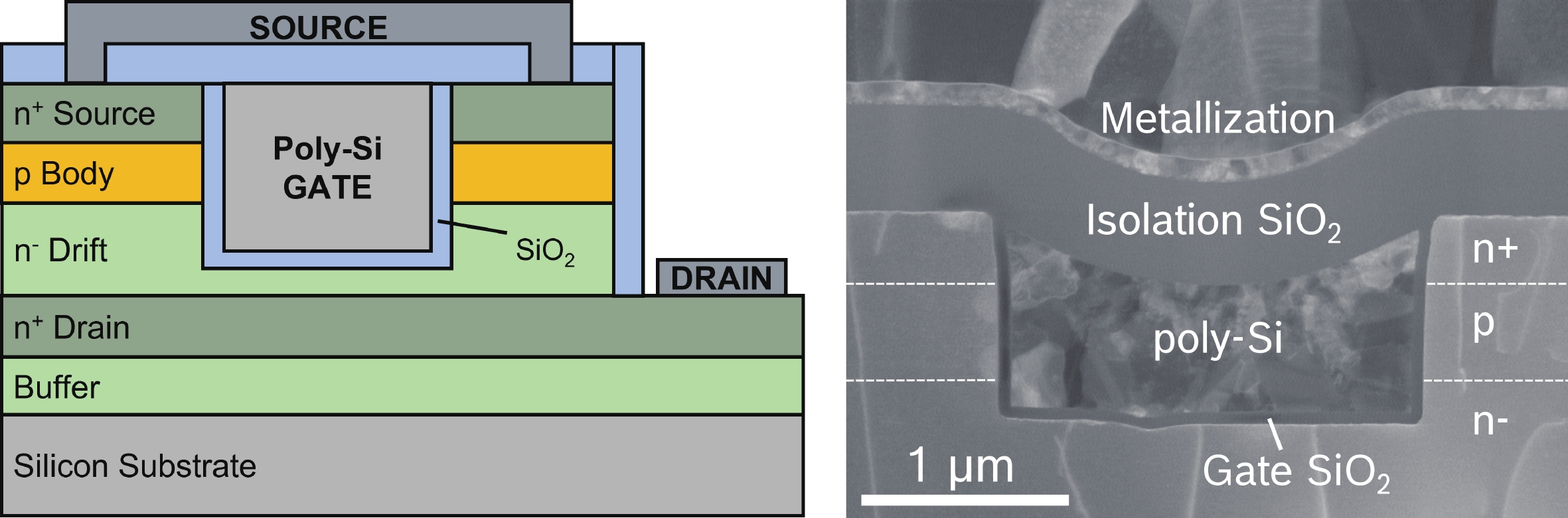
Fig. 1.
(Color online) (a) Schematic 2-D view of the pseudo-vertical GaN-on-Si TMOS under study in this work. (b) TEM image of a FIB lamella taken from the gate trench.
ARTICLES
Nicolò Zagni1, , Manuel Fregolent2, , Andrea Del Fiol2, Davide Favero2, Francesco Bergamin2, Giovanni Verzellesi3, 4, Carlo De Santi2, Gaudenzio Meneghesso2, Enrico Zanoni2, Christian Huber5, Matteo Meneghini2 and Paolo Pavan1
Corresponding author: Nicolò Zagni, nicolo.zagni@unimore.it; Manuel Fregolent, fregolentm@dei.unipd.it
Abstract: Vertical GaN power MOSFET is a novel technology that offers great potential for power switching applications. Being still in an early development phase, vertical GaN devices are yet to be fully optimized and require careful studies to foster their development. In this work, we report on the physical insights into device performance improvements obtained during the development of vertical GaN-on-Si trench MOSFETs (TMOS’s) provided by TCAD simulations, enhancing the dependability of the adopted process optimization approaches. Specifically, two different TMOS devices are compared in terms of transfer-curve hysteresis (H) and subthreshold slope (SS), showing a ≈ 75% H reduction along with a ≈ 30% SS decrease. Simulations allow attributing the achieved improvements to a decrease in the border and interface traps, respectively. A sensitivity analysis is also carried out, allowing to quantify the additional trap density reduction required to minimize both figures of merit.
Key words: vertical GaN trench MOSFET, SiO2, interface traps, border traps, hysteresis, BTI
| [1] |
Fu H Q, Fu K, Chowdhury S, et al. Vertical GaN power devices: Device principles and fabrication technologies—Part II. IEEE Trans Electron Devices, 2021, 68, 3212 doi: 10.1109/TED.2021.3083209
|
| [2] |
Meneghini M, De Santi C, Abid I, et al. GaN-based power devices: Physics, reliability, and perspectives. J Appl Phys, 2021, 130, 181101 doi: 10.1063/5.0061354
|
| [3] |
del Alamo J A, Lee E S. Stability and reliability of lateral GaN power field-effect transistors. IEEE Trans Electron Devices, 2019, 66, 4578 doi: 10.1109/TED.2019.2931718
|
| [4] |
Zagni N, Chini A, Puglisi F M, et al. “hole redistribution” model explaining the thermally activated RON stress/recovery transients in carbon-doped AlGaN/GaN power MIS-HEMTs. IEEE Trans Electron Devices, 2021, 68, 697 doi: 10.1109/TED.2020.3045683
|
| [5] |
Cioni M, Zagni N, Iucolano F, et al. Partial recovery of dynamic RON versus OFF-state stress voltage in p-GaN gate AlGaN/GaN power HEMTs. IEEE Trans Electron Devices, 2021, 68, 4862 doi: 10.1109/TED.2021.3105075
|
| [6] |
Chini A, Meneghesso G, Meneghini M, et al. Experimental and numerical analysis of hole emission process from carbon-related traps in GaN buffer layers. IEEE Trans Electron Devices, 2016, 63, 3473 doi: 10.1109/TED.2016.2593791
|
| [7] |
Modolo N, De Santi C, Minetto A, et al. A physics-based approach to model hot-electron trapping kinetics in p-GaN HEMTs. IEEE Electron Device Lett, 2021, 42, 673 doi: 10.1109/LED.2021.3067796
|
| [8] |
Ohnishi K, Kawasaki S, Fujimoto N, et al. Vertical GaN p+-n junction diode with ideal avalanche capability grown by halide vapor phase epitaxy. Appl Phys Lett, 2021, 119, 152102 doi: 10.1063/5.0066139
|
| [9] |
Bian Z L, Zeng K, Chowdhury S. 2.8 kV avalanche in vertical GaN PN diode utilizing field plate on hydrogen passivated P-layer. IEEE Electron Device Lett, 2022, 43, 596 doi: 10.1109/LED.2022.3149748
|
| [10] |
Liu J, Xiao M, Zhang Y, et al. 1.2 kV vertical GaN fin JFETs with robust avalanche and fast switching capabilities. 2020 IEEE International Electron Devices Meeting (IEDM), San Francisco, CA, USA. IEEE, 2021, 23.2. 1 doi: 10.1109/IEDM13553.2020.9372048
|
| [11] |
Mukherjee K, De Santi C, Borga M, et al. Challenges and perspectives for vertical GaN-on-Si trench MOS reliability: From leakage current analysis to gate stack optimization. Materials, 2021, 14, 2316 doi: 10.3390/ma14092316
|
| [12] |
Treidel E B, Hilt O, Hoffmann V, et al. On the conduction properties of vertical GaN n-channel trench MISFETs. IEEE J Electron Devices Soc, 2021, 9, 215 doi: 10.1109/JEDS.2021.3056697
|
| [13] |
Mukherjee K, De Santi C, Borga M, et al. Use of bilayer gate insulator in GaN-on-Si vertical trench MOSFETs: Impact on performance and reliability. Materials, 2020, 13, 4740 doi: 10.3390/ma13214740
|
| [14] |
Dannecker K, Baringhaus J. Fully vertical gallium nitride trench MOSFETs fabricated with metal-free gate first process. J Vac Sci Technol B, 2021, 39, 032204 doi: 10.1116/6.0000980
|
| [15] |
Henn M, Huber C. Impact of gate dielectric deposition temperature on p-type inversion channel MOSFETs fabricated on GaN-on-Si. 2022 IEEE Workshop on Wide Bandgap Power Devices and Applications in Europe (WiPDA Europe), 2022, 1 doi: 10.1109/WiPDAEurope55971.2022.9936574
|
| [16] |
Pavan P, Zagni N, Puglisi F M, et al. The impact of interface and border traps on current–voltage, capacitance–voltage, and split-CV mobility measurements in InGaAs MOSFETs. Phys Status Solidi A, 2017, 214, 1600592 doi: 10.1002/pssa.201600592
|
| [17] |
Guo A, del Alamo J A. Unified mechanism for positive- and negative-bias temperature instability in GaN MOSFETs. IEEE Trans Electron Devices, 2017, 64, 2142 doi: 10.1109/TED.2017.2686840
|
| [18] |
Wu T L, Franco J, Marcon D, et al. Toward understanding positive bias temperature instability in fully recessed-gate GaN MISFETs. IEEE Trans Electron Devices, 2016, 63, 1853 doi: 10.1109/TED.2016.2539341
|
| [19] |
Lagger P, Reiner M, Pogany D, et al. Comprehensive study of the complex dynamics of forward bias-induced threshold voltage drifts in GaN based MIS-HEMTs by stress/recovery experiments. IEEE Trans Electron Devices, 2014, 61, 1022 doi: 10.1109/TED.2014.2303853
|
| [20] |
Fregolent M, Del Fiol A, De Santi C, et al. Threshold voltage instability in SiO2-gate semi-vertical GaN trench MOSFETs grown on silicon substrate. Microelectron Reliab, 2023, 150, 115130 doi: 10.1016/j.microrel.2023.115130
|
| [21] |
Synopsys. Sentaurus SDevice manual (S-2021.06), 2021
|
| [22] |
Schroder D K. Oxide and interface trapped charges, oxide thickness. John Wiley & Sons, Inc. , 2005, 319
|
| [23] |
Sze S M, Ng K K. Physics of semiconductor devices. John Wiley & Sons, Inc. , 2006
|
| [24] |
Yu M Z, McNab S, Al-Dhahir I, et al. Extracting band-tail interface state densities from measurements and modelling of space charge layer resistance. Sol Energy Mater Sol Cells, 2021, 231, 111307 doi: 10.1016/j.solmat.2021.111307
|
| [25] |
Selmi L, Caruso E, Carapezzi S, et al. Modelling nanoscale n-MOSFETs with III-V compound semiconductor channels: From advanced models for band structures, electrostatics and transport to TCAD. 2017 IEEE International Electron Devices Meeting (IEDM), 2018, 13.4. 1 doi: 10.1109/IEDM.2017.8268384
|
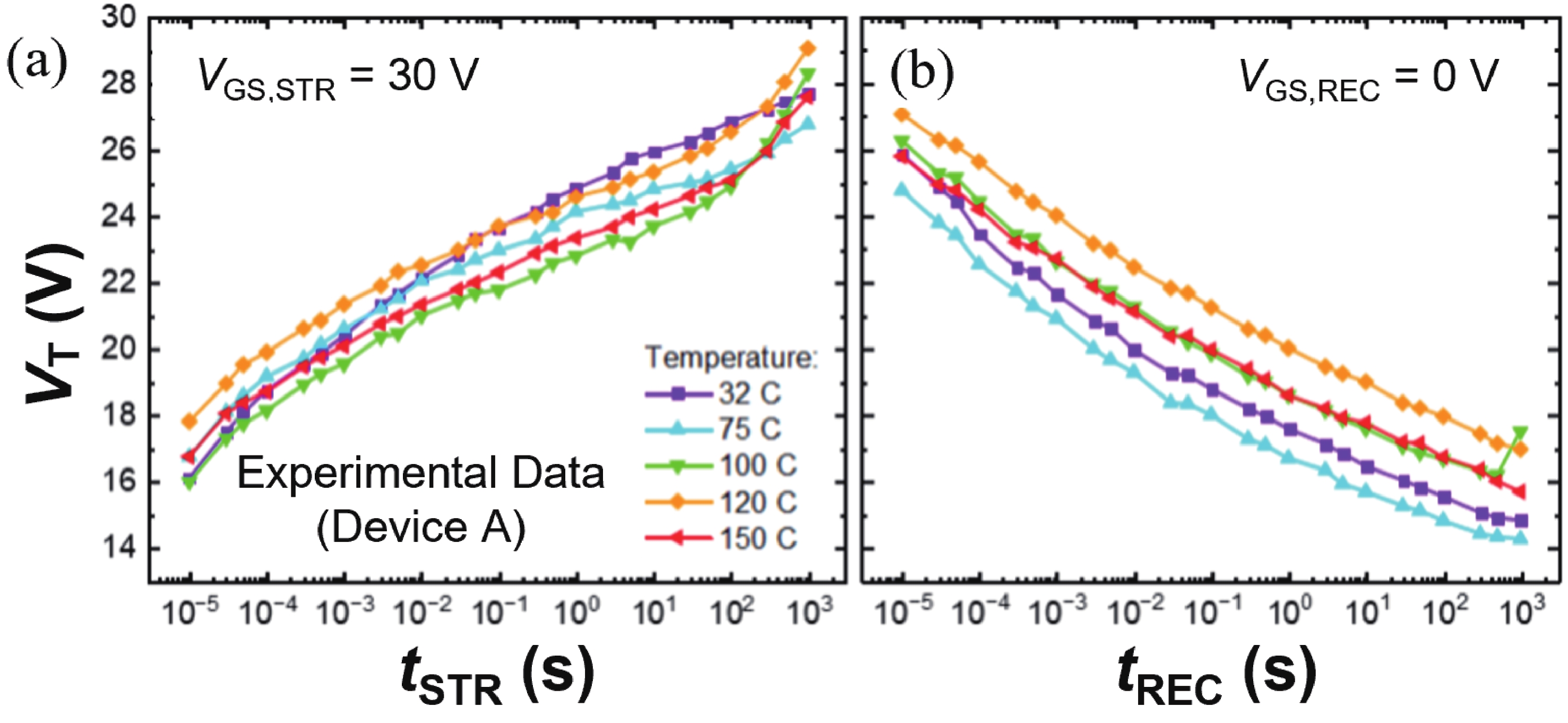
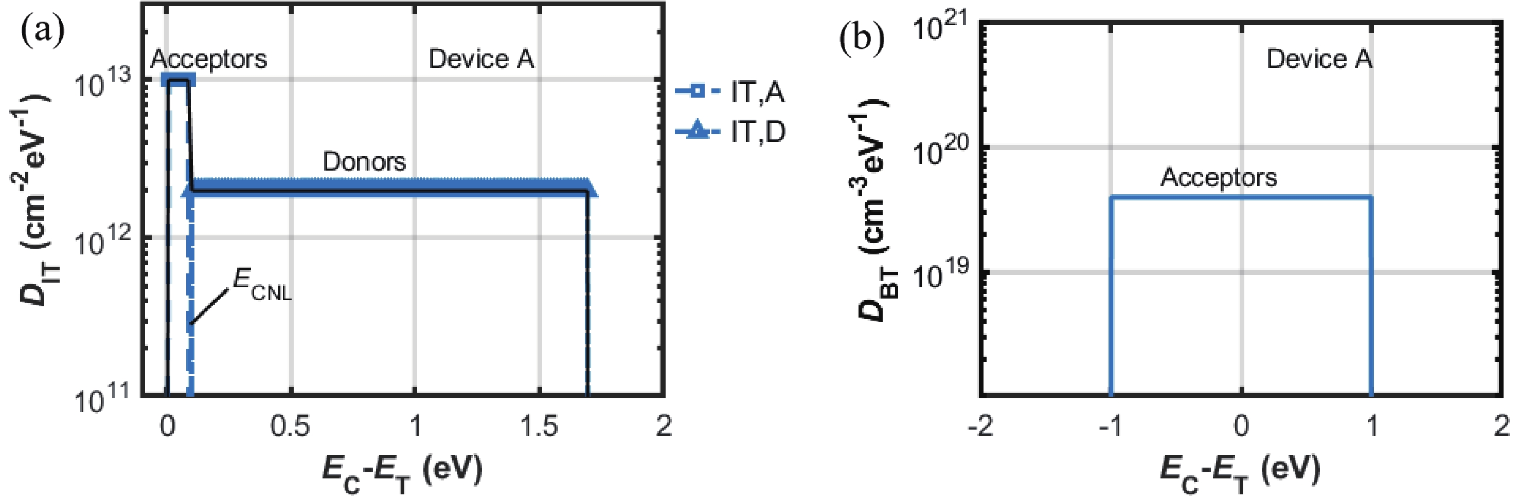
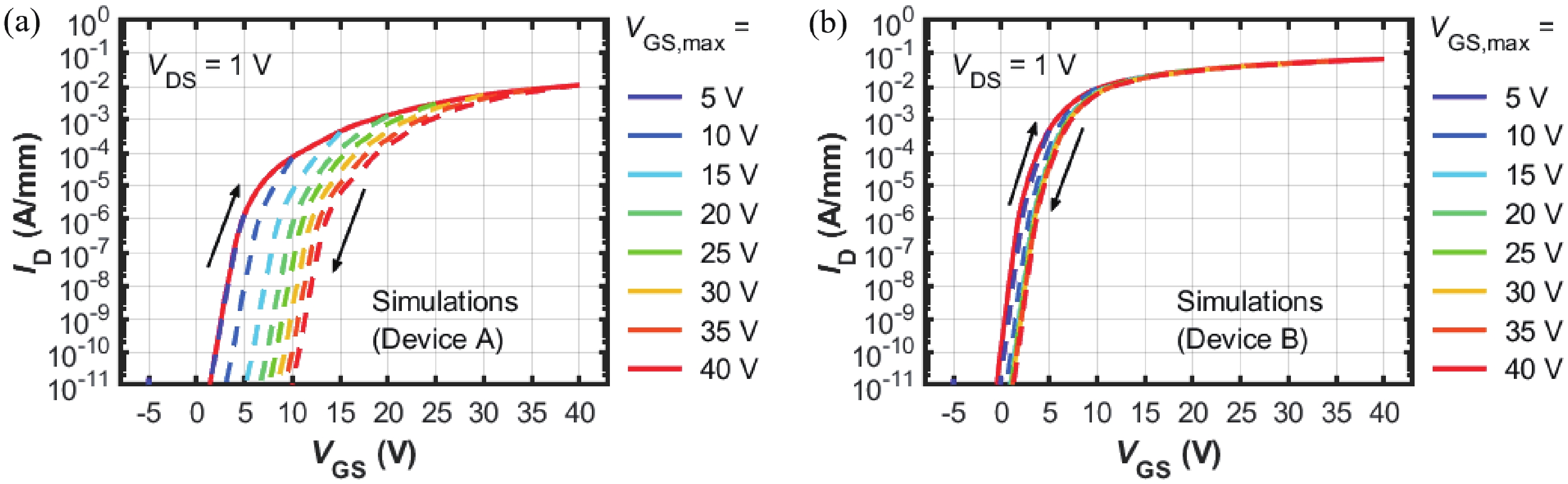
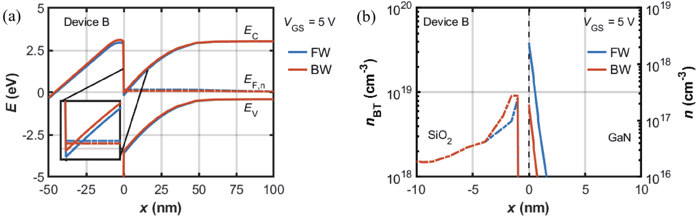
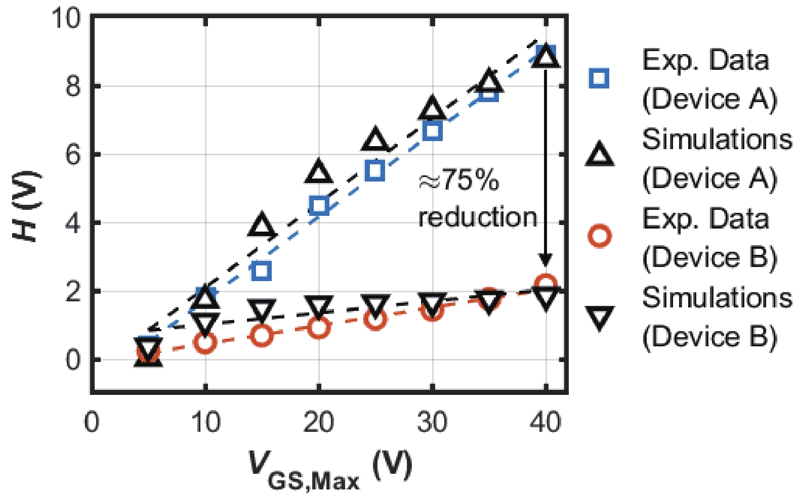
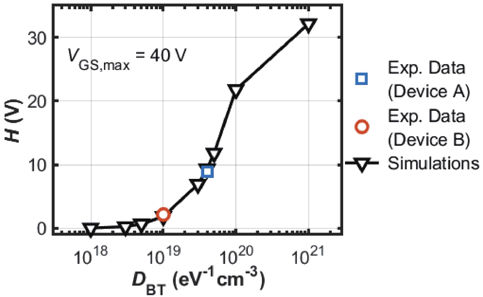
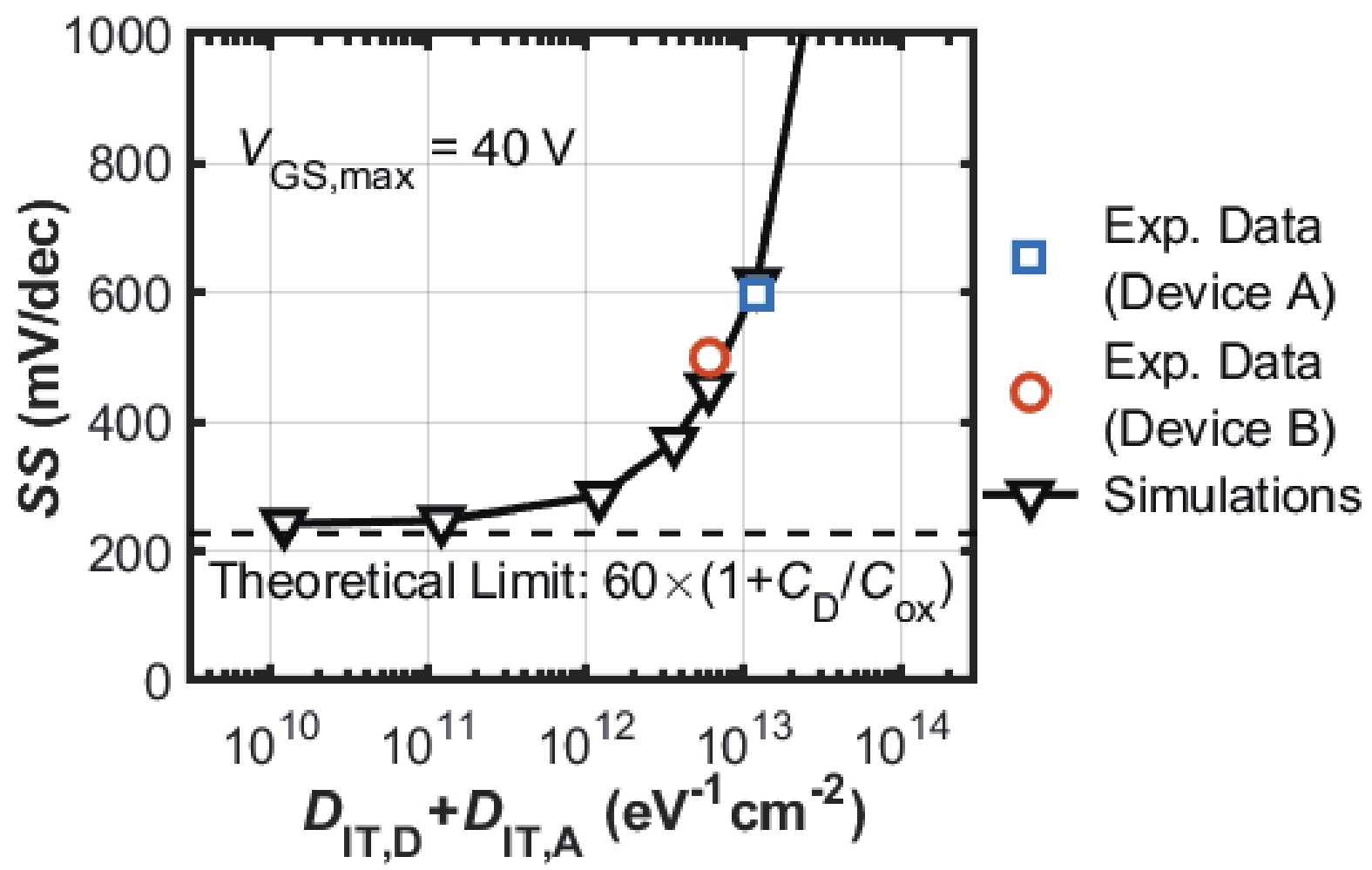
Table 1. Trap-related simulation parameters (Device A/Device B).
| Label* | Areal density (DIT, cm−2∙eV−1) | Volume density (DBT, cm−3∙eV−1) | Energy mean** (EM, eV) | Energy spread (ES, eV) |
| IT, A | 1 × 10¹³/5 × 1012 | // | 0 | 0.2 |
| IT, D | 2 × 10¹²/1 × 1012 | // | 0.9 | 1.6 |
| BT, A | // | 4 × 10¹⁹/1 × 1019 | 0 | 2 |
| *A stands for acceptors, D for donors. **With respect to GaN conduction band edge (EC). |
||||
 DownLoad: CSV
| [1] |
Fu H Q, Fu K, Chowdhury S, et al. Vertical GaN power devices: Device principles and fabrication technologies—Part II. IEEE Trans Electron Devices, 2021, 68, 3212 doi: 10.1109/TED.2021.3083209
|
| [2] |
Meneghini M, De Santi C, Abid I, et al. GaN-based power devices: Physics, reliability, and perspectives. J Appl Phys, 2021, 130, 181101 doi: 10.1063/5.0061354
|
| [3] |
del Alamo J A, Lee E S. Stability and reliability of lateral GaN power field-effect transistors. IEEE Trans Electron Devices, 2019, 66, 4578 doi: 10.1109/TED.2019.2931718
|
| [4] |
Zagni N, Chini A, Puglisi F M, et al. “hole redistribution” model explaining the thermally activated RON stress/recovery transients in carbon-doped AlGaN/GaN power MIS-HEMTs. IEEE Trans Electron Devices, 2021, 68, 697 doi: 10.1109/TED.2020.3045683
|
| [5] |
Cioni M, Zagni N, Iucolano F, et al. Partial recovery of dynamic RON versus OFF-state stress voltage in p-GaN gate AlGaN/GaN power HEMTs. IEEE Trans Electron Devices, 2021, 68, 4862 doi: 10.1109/TED.2021.3105075
|
| [6] |
Chini A, Meneghesso G, Meneghini M, et al. Experimental and numerical analysis of hole emission process from carbon-related traps in GaN buffer layers. IEEE Trans Electron Devices, 2016, 63, 3473 doi: 10.1109/TED.2016.2593791
|
| [7] |
Modolo N, De Santi C, Minetto A, et al. A physics-based approach to model hot-electron trapping kinetics in p-GaN HEMTs. IEEE Electron Device Lett, 2021, 42, 673 doi: 10.1109/LED.2021.3067796
|
| [8] |
Ohnishi K, Kawasaki S, Fujimoto N, et al. Vertical GaN p+-n junction diode with ideal avalanche capability grown by halide vapor phase epitaxy. Appl Phys Lett, 2021, 119, 152102 doi: 10.1063/5.0066139
|
| [9] |
Bian Z L, Zeng K, Chowdhury S. 2.8 kV avalanche in vertical GaN PN diode utilizing field plate on hydrogen passivated P-layer. IEEE Electron Device Lett, 2022, 43, 596 doi: 10.1109/LED.2022.3149748
|
| [10] |
Liu J, Xiao M, Zhang Y, et al. 1.2 kV vertical GaN fin JFETs with robust avalanche and fast switching capabilities. 2020 IEEE International Electron Devices Meeting (IEDM), San Francisco, CA, USA. IEEE, 2021, 23.2. 1 doi: 10.1109/IEDM13553.2020.9372048
|
| [11] |
Mukherjee K, De Santi C, Borga M, et al. Challenges and perspectives for vertical GaN-on-Si trench MOS reliability: From leakage current analysis to gate stack optimization. Materials, 2021, 14, 2316 doi: 10.3390/ma14092316
|
| [12] |
Treidel E B, Hilt O, Hoffmann V, et al. On the conduction properties of vertical GaN n-channel trench MISFETs. IEEE J Electron Devices Soc, 2021, 9, 215 doi: 10.1109/JEDS.2021.3056697
|
| [13] |
Mukherjee K, De Santi C, Borga M, et al. Use of bilayer gate insulator in GaN-on-Si vertical trench MOSFETs: Impact on performance and reliability. Materials, 2020, 13, 4740 doi: 10.3390/ma13214740
|
| [14] |
Dannecker K, Baringhaus J. Fully vertical gallium nitride trench MOSFETs fabricated with metal-free gate first process. J Vac Sci Technol B, 2021, 39, 032204 doi: 10.1116/6.0000980
|
| [15] |
Henn M, Huber C. Impact of gate dielectric deposition temperature on p-type inversion channel MOSFETs fabricated on GaN-on-Si. 2022 IEEE Workshop on Wide Bandgap Power Devices and Applications in Europe (WiPDA Europe), 2022, 1 doi: 10.1109/WiPDAEurope55971.2022.9936574
|
| [16] |
Pavan P, Zagni N, Puglisi F M, et al. The impact of interface and border traps on current–voltage, capacitance–voltage, and split-CV mobility measurements in InGaAs MOSFETs. Phys Status Solidi A, 2017, 214, 1600592 doi: 10.1002/pssa.201600592
|
| [17] |
Guo A, del Alamo J A. Unified mechanism for positive- and negative-bias temperature instability in GaN MOSFETs. IEEE Trans Electron Devices, 2017, 64, 2142 doi: 10.1109/TED.2017.2686840
|
| [18] |
Wu T L, Franco J, Marcon D, et al. Toward understanding positive bias temperature instability in fully recessed-gate GaN MISFETs. IEEE Trans Electron Devices, 2016, 63, 1853 doi: 10.1109/TED.2016.2539341
|
| [19] |
Lagger P, Reiner M, Pogany D, et al. Comprehensive study of the complex dynamics of forward bias-induced threshold voltage drifts in GaN based MIS-HEMTs by stress/recovery experiments. IEEE Trans Electron Devices, 2014, 61, 1022 doi: 10.1109/TED.2014.2303853
|
| [20] |
Fregolent M, Del Fiol A, De Santi C, et al. Threshold voltage instability in SiO2-gate semi-vertical GaN trench MOSFETs grown on silicon substrate. Microelectron Reliab, 2023, 150, 115130 doi: 10.1016/j.microrel.2023.115130
|
| [21] |
Synopsys. Sentaurus SDevice manual (S-2021.06), 2021
|
| [22] |
Schroder D K. Oxide and interface trapped charges, oxide thickness. John Wiley & Sons, Inc. , 2005, 319
|
| [23] |
Sze S M, Ng K K. Physics of semiconductor devices. John Wiley & Sons, Inc. , 2006
|
| [24] |
Yu M Z, McNab S, Al-Dhahir I, et al. Extracting band-tail interface state densities from measurements and modelling of space charge layer resistance. Sol Energy Mater Sol Cells, 2021, 231, 111307 doi: 10.1016/j.solmat.2021.111307
|
| [25] |
Selmi L, Caruso E, Carapezzi S, et al. Modelling nanoscale n-MOSFETs with III-V compound semiconductor channels: From advanced models for band structures, electrostatics and transport to TCAD. 2017 IEEE International Electron Devices Meeting (IEDM), 2018, 13.4. 1 doi: 10.1109/IEDM.2017.8268384
|


Article views: 3618 Times PDF downloads: 470 Times Cited by: 0 Times
Received: 22 July 2023 Revised: 19 October 2023 Online: Accepted Manuscript: 06 December 2023Uncorrected proof: 08 December 2023Published: 15 March 2024
| Citation: |
Nicolò Zagni, Manuel Fregolent, Andrea Del Fiol, Davide Favero, Francesco Bergamin, Giovanni Verzellesi, Carlo De Santi, Gaudenzio Meneghesso, Enrico Zanoni, Christian Huber, Matteo Meneghini, Paolo Pavan. Physical insights into trapping effects on vertical GaN-on-Si trench MOSFETs from TCAD[J]. Journal of Semiconductors, 2024, 45(3): 032501. doi: 10.1088/1674-4926/45/3/032501
****
N Zagni, M Fregolent, A D Fiol, D Favero, F Bergamin, G Verzellesi, C D Santi, G Meneghesso, E Zanoni, C Huber, M Meneghini, P Pavan. Physical insights into trapping effects on vertical GaN-on-Si trench MOSFETs from TCAD[J]. J. Semicond, 2024, 45(3): 032501. doi: 10.1088/1674-4926/45/3/032501

|
 Nicolò Zagni is a postdoc researcher at University of Modena and Reggio Emilia. In 2021 he received the PhD degree in electrical engineering from the same institution. In 2018 and 2019 he was a visiting scholar at Purdue University, USA. His research interests are in the investigation of novel electron devices and circuits for applications such as digital logic, power conversion, non-volatile memory, and biosensors. His current research is focused on the modeling of stability and reliability of GaN HEMTs for power applications and reliability of Ferroelectric FETs
 Giovanni Verzellesi received the “Laurea” degree in electrical engineering from the University of Bologna, Bologna, Italy, in 1989, and the Ph.D. degree also in electrical engineering from the University of Padova, Padova, Italy, in 1994. In 1993–1994, he was a visiting graduate student with the University of California, Santa Barbara (CA, USA). From 1994 to 1999, he was with the University of Trento, Italy, as an assistant professor of Electronics. Since 1999, he has been with the University of Modena and Reggio Emilia, Italy, where he became associate professor in 2000 and professor in 2006
 Carlo De Santi since September 2019, holds an assistant professor position at the University of Padova. His main research activities focus on the characterization, modeling of physical processes, and reliability of electronic and optoelectronic devices based on elemental and compound semiconductors, including various ternary and quaternary compounds. The application fields of interest are power electronics and radio frequency systems, LEDs and lasers in the UV, visible monochromatic and white spectral range, devices for silicon photonics, solar cells and photodetectors, and phosphors and systems for lighting applications. He is a co-author of more than 250 journal and conference papers, including 43 invited ones
 Gaudenzio Meneghesso graduated in electronics engineering at the University of Padova in 1992 working on the failure mechanism induced by hot electrons in MESFET sand HEMTs. Since 2011, he is with University of Padova as full professor. His research interests involve mainly the electrical characterization, modeling, and reliability of microelectronics devices. Within these activities, he published more than 800 technical papers (of which more than 100 invited papers and 12 best paper awards). He has been nominated to IEEE Fellow class 2013, with the following citation: “for contributions to the reliability physics of compound semiconductors devices”
 Enrico Zanoni is professor of microelectronics at the Department of Information Engineering of the University of Padova since 1993 and an IEEE Fellow since 2009. At the University of Padova, he contributed to establish a research group involved in CMOS analog and rf-integrated circuit design, CMOS reliability and radiation hardness, compound semiconductor characterization, modeling, and reliability. Enrico Zanoni is coauthor of more than 800 publications on the modeling and reliability physics of silicon and compound semiconductor devices and of 4 patents
 Christian Huber received his Ph.D. degree in physics from Karlsruhe Institute of Technology, Karlsruhe, Germany in 2019. His current research activity is in the field of wide band gap power electronics with special focus on vertical GaN power transistor concepts and GaN process technology. He is project coordinator of the EU-funded project YESvGaN and is actively involved in the development of front and backside process technology for vertical GaN-on-silicon membrane transistors. Dr. Huber was awarded with the Thomas Gessner Award for excellent scientific theses in the field of Smart Systems Integration in 2019
 Matteo Meneghini received the Ph.D. degree from the University of Padua, Padua, Italy, in 2008, with a focus on the optimization of gallium nitride (GaN)-based LED and laser structures. He is currently a Full Professor with the Department of Information Engineering, University of Padua. His main interests are the characterization, reliability, and modeling of compound semiconductor devices [LEDs, laser diodes, and high electron mobility transistors (HEMTs)], and optoelectronic components, including solar cells. Within these activities, he has published more than 400 journal articles and conference proceedings papers
 Paolo Pavan is Full Professor of electronics with the University of Modena and Reggio Emilia. He is currently Rector’s Delegate for Scientific Research, he has been the Dean of the Electronics Engineering Program and he also served as several academic appointments. His research interests are in the characterization, modeling and optimization of nonvolatile memory devices, more recently RRAMs. From this last activity, he started to investigate Logic-in-Memory and neuromorphic architectures. He is also involved in the development of safety critical and energy-aware applications for low-power computing and automotive electronics. He is an Associate Editor of IEEE Journal of Electron Device Society
| [1] |
Fu H Q, Fu K, Chowdhury S, et al. Vertical GaN power devices: Device principles and fabrication technologies—Part II. IEEE Trans Electron Devices, 2021, 68, 3212 doi: 10.1109/TED.2021.3083209
|
| [2] |
Meneghini M, De Santi C, Abid I, et al. GaN-based power devices: Physics, reliability, and perspectives. J Appl Phys, 2021, 130, 181101 doi: 10.1063/5.0061354
|
| [3] |
del Alamo J A, Lee E S. Stability and reliability of lateral GaN power field-effect transistors. IEEE Trans Electron Devices, 2019, 66, 4578 doi: 10.1109/TED.2019.2931718
|
| [4] |
Zagni N, Chini A, Puglisi F M, et al. “hole redistribution” model explaining the thermally activated RON stress/recovery transients in carbon-doped AlGaN/GaN power MIS-HEMTs. IEEE Trans Electron Devices, 2021, 68, 697 doi: 10.1109/TED.2020.3045683
|
| [5] |
Cioni M, Zagni N, Iucolano F, et al. Partial recovery of dynamic RON versus OFF-state stress voltage in p-GaN gate AlGaN/GaN power HEMTs. IEEE Trans Electron Devices, 2021, 68, 4862 doi: 10.1109/TED.2021.3105075
|
| [6] |
Chini A, Meneghesso G, Meneghini M, et al. Experimental and numerical analysis of hole emission process from carbon-related traps in GaN buffer layers. IEEE Trans Electron Devices, 2016, 63, 3473 doi: 10.1109/TED.2016.2593791
|
| [7] |
Modolo N, De Santi C, Minetto A, et al. A physics-based approach to model hot-electron trapping kinetics in p-GaN HEMTs. IEEE Electron Device Lett, 2021, 42, 673 doi: 10.1109/LED.2021.3067796
|
| [8] |
Ohnishi K, Kawasaki S, Fujimoto N, et al. Vertical GaN p+-n junction diode with ideal avalanche capability grown by halide vapor phase epitaxy. Appl Phys Lett, 2021, 119, 152102 doi: 10.1063/5.0066139
|
| [9] |
Bian Z L, Zeng K, Chowdhury S. 2.8 kV avalanche in vertical GaN PN diode utilizing field plate on hydrogen passivated P-layer. IEEE Electron Device Lett, 2022, 43, 596 doi: 10.1109/LED.2022.3149748
|
| [10] |
Liu J, Xiao M, Zhang Y, et al. 1.2 kV vertical GaN fin JFETs with robust avalanche and fast switching capabilities. 2020 IEEE International Electron Devices Meeting (IEDM), San Francisco, CA, USA. IEEE, 2021, 23.2. 1 doi: 10.1109/IEDM13553.2020.9372048
|
| [11] |
Mukherjee K, De Santi C, Borga M, et al. Challenges and perspectives for vertical GaN-on-Si trench MOS reliability: From leakage current analysis to gate stack optimization. Materials, 2021, 14, 2316 doi: 10.3390/ma14092316
|
| [12] |
Treidel E B, Hilt O, Hoffmann V, et al. On the conduction properties of vertical GaN n-channel trench MISFETs. IEEE J Electron Devices Soc, 2021, 9, 215 doi: 10.1109/JEDS.2021.3056697
|
| [13] |
Mukherjee K, De Santi C, Borga M, et al. Use of bilayer gate insulator in GaN-on-Si vertical trench MOSFETs: Impact on performance and reliability. Materials, 2020, 13, 4740 doi: 10.3390/ma13214740
|
| [14] |
Dannecker K, Baringhaus J. Fully vertical gallium nitride trench MOSFETs fabricated with metal-free gate first process. J Vac Sci Technol B, 2021, 39, 032204 doi: 10.1116/6.0000980
|
| [15] |
Henn M, Huber C. Impact of gate dielectric deposition temperature on p-type inversion channel MOSFETs fabricated on GaN-on-Si. 2022 IEEE Workshop on Wide Bandgap Power Devices and Applications in Europe (WiPDA Europe), 2022, 1 doi: 10.1109/WiPDAEurope55971.2022.9936574
|
| [16] |
Pavan P, Zagni N, Puglisi F M, et al. The impact of interface and border traps on current–voltage, capacitance–voltage, and split-CV mobility measurements in InGaAs MOSFETs. Phys Status Solidi A, 2017, 214, 1600592 doi: 10.1002/pssa.201600592
|
| [17] |
Guo A, del Alamo J A. Unified mechanism for positive- and negative-bias temperature instability in GaN MOSFETs. IEEE Trans Electron Devices, 2017, 64, 2142 doi: 10.1109/TED.2017.2686840
|
| [18] |
Wu T L, Franco J, Marcon D, et al. Toward understanding positive bias temperature instability in fully recessed-gate GaN MISFETs. IEEE Trans Electron Devices, 2016, 63, 1853 doi: 10.1109/TED.2016.2539341
|
| [19] |
Lagger P, Reiner M, Pogany D, et al. Comprehensive study of the complex dynamics of forward bias-induced threshold voltage drifts in GaN based MIS-HEMTs by stress/recovery experiments. IEEE Trans Electron Devices, 2014, 61, 1022 doi: 10.1109/TED.2014.2303853
|
| [20] |
Fregolent M, Del Fiol A, De Santi C, et al. Threshold voltage instability in SiO2-gate semi-vertical GaN trench MOSFETs grown on silicon substrate. Microelectron Reliab, 2023, 150, 115130 doi: 10.1016/j.microrel.2023.115130
|
| [21] |
Synopsys. Sentaurus SDevice manual (S-2021.06), 2021
|
| [22] |
Schroder D K. Oxide and interface trapped charges, oxide thickness. John Wiley & Sons, Inc. , 2005, 319
|
| [23] |
Sze S M, Ng K K. Physics of semiconductor devices. John Wiley & Sons, Inc. , 2006
|
| [24] |
Yu M Z, McNab S, Al-Dhahir I, et al. Extracting band-tail interface state densities from measurements and modelling of space charge layer resistance. Sol Energy Mater Sol Cells, 2021, 231, 111307 doi: 10.1016/j.solmat.2021.111307
|
| [25] |
Selmi L, Caruso E, Carapezzi S, et al. Modelling nanoscale n-MOSFETs with III-V compound semiconductor channels: From advanced models for band structures, electrostatics and transport to TCAD. 2017 IEEE International Electron Devices Meeting (IEDM), 2018, 13.4. 1 doi: 10.1109/IEDM.2017.8268384
|

 WeChat ID
Journal of Semiconductors © 2017 All Rights Reserved 京ICP备05085259号-2


