


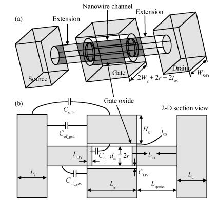
Fig. 1.
(a) 3D view of a cylindrical surrounding gate MOSFET with (b) different parasitic capacitances[19].
SEMICONDUCTOR DEVICES
Abstract: A physically based analytical model for surface potential and threshold voltage including the fringing gate capacitances in cylindrical surround gate (CSG) MOSFETs has been developed. Based on this a subthreshold drain current model has also been derived. This model first computes the charge induced in the drain/source region due to the fringing capacitances and considers an effective charge distribution in the cylindrically extended source/drain region for the development of a simple and compact model. The fringing gate capacitances taken into account are outer fringe capacitance, inner fringe capacitance, overlap capacitance, and sidewall capacitance. The model has been verified with the data extracted from 3D TCAD simulations of CSG MOSFETs and was found to be working satisfactorily.
Keywords: physics based modeling, source/drain extension (SDE), cylindrical surrounding gate (CSG) MOSFETs, fringing field, surface potential, threshold voltage
| [1] |
Shrivastava R, Fitzpatrick K. A simple model for the overlap capacitance of a VLSI MOS device. IEEE Trans Electron Devices, 1982, 29(12):1870 doi: 10.1109/T-ED.1982.21044
|
| [2] |
Greeneich E W. An analytical model for the gate capacitance of small-geometry MOS structures. IEEE Trans Electron Devices, 1983, 30(12):1838 doi: 10.1109/T-ED.1983.21456
|
| [3] |
Suzuki K. Parasitic capacitance of submicrometer MOSFET's. IEEE Trans Electron Devices, 1999, 46(9):1895 doi: 10.1109/16.784191
|
| [4] |
Mohapatra N R, Desai M P, Narendra S G, et al. Modeling of parasitic capacitances in deep submicrometer conventional and high-k dielectric MOS transistors. IEEE Trans Electron Devices, 2003, 50(4):959 doi: 10.1109/TED.2003.811387
|
| [5] |
Kumar M J, Gupta S K, Venkataraman V. Compact modeling of the effects of parasitic internal fringe capacitance on the threshold voltage of high-k gate-dielectric nanoscale SOI MOSFETs. IEEE Trans Electron Devices, 2006, 53(4):706 doi: 10.1109/TED.2006.870424
|
| [6] |
Bansal A, Paul B C, Roy K. Modeling and optimization of fringe capacitance of nanoscale DGMOS devices. IEEE Trans Electron Devices, 2005, 52(2):256 doi: 10.1109/TED.2004.842713
|
| [7] |
Guo J C, Yeh C T. A new three-dimensional capacitor model for accurate simulation of parasitic capacitances in nanoscale MOSFETs. IEEE Trans Electron Devices, 2009, 56(8):1598 doi: 10.1109/TED.2009.2022679
|
| [8] |
Liu X, Jin X, Lee J H, et al. A full analytical model of fringing-field-induced parasitic capacitance for nano-scaled MOSFETs. Semicond Sci Technol, 2010, 25(12):015008 http://info.scichina.com:8084/sciF/EN/abstract/abstract515018.shtml
|
| [9] |
Sun J P, Wang W, Toyabe T, et al. Modeling of gate current and capacitance in nanoscale-MOS structures. IEEE Trans Electron Devices, 2006, 53(12):2950 doi: 10.1109/TED.2006.885637
|
| [10] |
Ernst T, Ritzenthaler R, Faynot O, et al. A model of fringing fields in short-channel planar and triple-gate SOI MOSFETs. IEEE Trans Electron Devices, 2007, 54(6):1366 doi: 10.1109/TED.2007.895241
|
| [11] |
Kumar M J, Venkataraman V, Gupta S K. On the parasitic gate capacitance of small-geometry MOSFETs. IEEE Trans Electron Devices, 2005, 52(7):1676 doi: 10.1109/TED.2005.850630
|
| [12] |
Guo J C, Yeh C T. A new three-dimensional capacitor model for accurate simulation of parasitic capacitances in nanoscale MOSFETs. IEEE Trans Electron Devices, 2009, 56(8):1598 doi: 10.1109/TED.2009.2022679
|
| [13] |
Moldovan O, Iñiguez B, Jiménez D, et al. Analytical charge and capacitance models of undoped cylindrical surrounding-gate MOSFETs. IEEE Trans Electron Devices, 2007, 54(1):162 doi: 10.1109/TED.2006.887213
|
| [14] |
He J, Bian W, Tao Y, et al. Analytic carrier-based charge and capacitance model for long-channel undoped surrounding-gate MOSFETs. IEEE Trans Electron Devices, 2007, 54(6):1478 doi: 10.1109/TED.2007.896595
|
| [15] |
Jiménez D, Iñíguez B, Suñél J, et al. Continuous analytic Ⅰ-Ⅴ model for surrounding-gate MOSFETs. IEEE Electron Device Lett, 2004, 25(8):571 doi: 10.1109/LED.2004.831902
|
| [16] |
Sarkar A, De S, Dey A, et al. A new analytical subthreshold model of SRG MOSFET with analogue performance investigation. International Journal of Electronics, 2012, 99(2):267 doi: 10.1080/00207217.2011.623278
|
| [17] |
Xu Q, Zou J, Luo J, et al. Predictive modeling of capacitance and resistance in gate all around cylindrical nanowire MOSFETs for parasitic design optimization. 10th IEEE International Conference on Solid State and Integrated Circuit Technology (ICSICT), Shanghai, 2010:1958 http://www.academia.edu/842570/Predictive_modeling_of_capacitance_and_resistance_in_gate-all-around_cylindrical_nanowire_MOSFETs_for_parasitic_design_optimization
|
| [18] |
Sarkar A, De S, Dey A, et al. Analog and RF performance investigation of cylindrical surrounding-gate MOSFET with an analytical pseudo-2D model. J Comput Electron, 2012, 11(2):182 doi: 10.1007/s10825-012-0396-9
|
| [19] |
Zou J, Xu Q, Luo J, et al. Predictive 3-D modeling of parasitic gate capacitance in gate-all-around cylindrical silicon nanowire MOSFETs. IEEE Trans Electron Devices, 2011, 58(10):3379 doi: 10.1109/TED.2011.2162521
|
| [20] |
Ge L, Fossum J G. Analytical modeling of quantization and volume inversion in thin Si-film DG MOSFETs. IEEE Trans Electron Devices, 2002, 49(2):287 doi: 10.1109/16.981219
|
| [21] |
Chiang T K. Concise analytical threshold voltage model for cylindrical fully depleted surrounding-gate metal-oxide-semiconductor field effect transistors. Jpn J Appl Phys, 2005, 44(5):2948 doi: 10.1143/JJAP.44.2948
|
| [22] |
Kaur H, Kabra S, Haldar S, et al. An analytical threshold voltage model for graded channel asymmetric gate stack (GCASYSMGAS) surrounding gate MOSFET. Solid-State Electron, 2008, 52(2):305 doi: 10.1016/j.sse.2007.09.006
|
| [23] |
Auth C P, Plummer J D. Scaling theory for cylindrical fully-depleted surrounding gate MOSFET's. IEEE Electron Device Lett, 1997, 18(2):74 doi: 10.1109/55.553049
|
| [24] |
Kranti A, Haldar S, Gupta R S. Analytical model for threshold voltage and Ⅰ-Ⅴ characteristics of fully depleted short channel cylindrical/surrounding gate MOSFET. Microelectron Eng, 2001, 56:241 doi: 10.1016/S0167-9317(00)00419-6
|
| [25] |
Faycal D, Mohamed Amir A, Djemai A, et al. Surface-potential-based model to study the subthreshold swing behavior including hot-carrier effect for nanoscale GASGAA MOSFETs. International conference on Design & Technology of Integrated Systems in Nanoscale Era, 2010:1 http://yadda.icm.edu.pl/yadda/element/bwmeta1.element.ieee-year-000005481254-2010
|
| [26] |
Young K K. Analysis of conduction in fully depleted SOI MOSFETs. IEEE Trans Electron Devices, 1989, 36:504 doi: 10.1109/16.19960
|
| [27] |
Gupta S K, Baishya S. Modeling and simulation of triple metal cylindrical surround gate MOSFETs for reduced short channel effects. International Journal of Soft Computing and Engineering (IJSCE), 2012, 2(2):214 doi: 10.1007%2Fs10825-014-0576-x.pdf
|
| [28] |
Gupta S K, Baishya S. Modeling of built-in potential variations of cylindrical surrounding gate (CSG) MOSFETs. International Journal of VLSI Design and Communication Systems (VLSIC), 2012, 3(5):67 doi: 10.5121/vlsic
|
| [29] |
Byerly W E. Elements of the integral calculus with a key to the solution of differential equations, and a short table of integrals. 2nd ed. Boston USA:Ginn and Company, 1892
|
| [30] |
Jahnke E, Emde F. Tables of functions with formulae and curves. Dover Publications, 1943 http://www.worldcat.org/title/tables-of-functions-with-formulae-and-curves/oclc/6368281
|
| [31] |
Nehari Z. Conformal mapping. McGraw-Hill, 1952
|
| [32] |
Kober H. Dictionary of conformal representations. Dover Publications, 1957 http://www.worldcat.org/title/dictionary-of-conformal-representations/oclc/14246040
|
| [33] |
Dwight H B. Tables of integrals and other mathematical data. 3rd ed. New York, USA:The Macmillan Company, 1957
|
| [34] |
Churchill R V, Brown J W, Verhey R F. Complex variables and applications. 3rd ed. McGraw Hill, 1976
|
| [35] |
Smythe W R. Static and dynamic electricity. 3rd ed. Taylor & Francis, 1989 doi: 10.1007/978-88-470-5647-3_7
|


Article views: 3413 Times PDF downloads: 45 Times Cited by: 0 Times
Received: 15 December 2012 Revised: 25 January 2013 Online: Published: 01 July 2013
| Citation: |
Santosh K. Gupta, Srimanta Baishya. Modeling of cylindrical surrounding gate MOSFETs including the fringing field effects[J]. Journal of Semiconductors, 2013, 34(7): 074001. doi: 10.1088/1674-4926/34/7/074001
****
S K Gupta, S Baishya. Modeling of cylindrical surrounding gate MOSFETs including the fringing field effects[J]. J. Semicond., 2013, 34(7): 074001. doi: 10.1088/1674-4926/34/7/074001.

|
| [1] |
Shrivastava R, Fitzpatrick K. A simple model for the overlap capacitance of a VLSI MOS device. IEEE Trans Electron Devices, 1982, 29(12):1870 doi: 10.1109/T-ED.1982.21044
|
| [2] |
Greeneich E W. An analytical model for the gate capacitance of small-geometry MOS structures. IEEE Trans Electron Devices, 1983, 30(12):1838 doi: 10.1109/T-ED.1983.21456
|
| [3] |
Suzuki K. Parasitic capacitance of submicrometer MOSFET's. IEEE Trans Electron Devices, 1999, 46(9):1895 doi: 10.1109/16.784191
|
| [4] |
Mohapatra N R, Desai M P, Narendra S G, et al. Modeling of parasitic capacitances in deep submicrometer conventional and high-k dielectric MOS transistors. IEEE Trans Electron Devices, 2003, 50(4):959 doi: 10.1109/TED.2003.811387
|
| [5] |
Kumar M J, Gupta S K, Venkataraman V. Compact modeling of the effects of parasitic internal fringe capacitance on the threshold voltage of high-k gate-dielectric nanoscale SOI MOSFETs. IEEE Trans Electron Devices, 2006, 53(4):706 doi: 10.1109/TED.2006.870424
|
| [6] |
Bansal A, Paul B C, Roy K. Modeling and optimization of fringe capacitance of nanoscale DGMOS devices. IEEE Trans Electron Devices, 2005, 52(2):256 doi: 10.1109/TED.2004.842713
|
| [7] |
Guo J C, Yeh C T. A new three-dimensional capacitor model for accurate simulation of parasitic capacitances in nanoscale MOSFETs. IEEE Trans Electron Devices, 2009, 56(8):1598 doi: 10.1109/TED.2009.2022679
|
| [8] |
Liu X, Jin X, Lee J H, et al. A full analytical model of fringing-field-induced parasitic capacitance for nano-scaled MOSFETs. Semicond Sci Technol, 2010, 25(12):015008 http://info.scichina.com:8084/sciF/EN/abstract/abstract515018.shtml
|
| [9] |
Sun J P, Wang W, Toyabe T, et al. Modeling of gate current and capacitance in nanoscale-MOS structures. IEEE Trans Electron Devices, 2006, 53(12):2950 doi: 10.1109/TED.2006.885637
|
| [10] |
Ernst T, Ritzenthaler R, Faynot O, et al. A model of fringing fields in short-channel planar and triple-gate SOI MOSFETs. IEEE Trans Electron Devices, 2007, 54(6):1366 doi: 10.1109/TED.2007.895241
|
| [11] |
Kumar M J, Venkataraman V, Gupta S K. On the parasitic gate capacitance of small-geometry MOSFETs. IEEE Trans Electron Devices, 2005, 52(7):1676 doi: 10.1109/TED.2005.850630
|
| [12] |
Guo J C, Yeh C T. A new three-dimensional capacitor model for accurate simulation of parasitic capacitances in nanoscale MOSFETs. IEEE Trans Electron Devices, 2009, 56(8):1598 doi: 10.1109/TED.2009.2022679
|
| [13] |
Moldovan O, Iñiguez B, Jiménez D, et al. Analytical charge and capacitance models of undoped cylindrical surrounding-gate MOSFETs. IEEE Trans Electron Devices, 2007, 54(1):162 doi: 10.1109/TED.2006.887213
|
| [14] |
He J, Bian W, Tao Y, et al. Analytic carrier-based charge and capacitance model for long-channel undoped surrounding-gate MOSFETs. IEEE Trans Electron Devices, 2007, 54(6):1478 doi: 10.1109/TED.2007.896595
|
| [15] |
Jiménez D, Iñíguez B, Suñél J, et al. Continuous analytic Ⅰ-Ⅴ model for surrounding-gate MOSFETs. IEEE Electron Device Lett, 2004, 25(8):571 doi: 10.1109/LED.2004.831902
|
| [16] |
Sarkar A, De S, Dey A, et al. A new analytical subthreshold model of SRG MOSFET with analogue performance investigation. International Journal of Electronics, 2012, 99(2):267 doi: 10.1080/00207217.2011.623278
|
| [17] |
Xu Q, Zou J, Luo J, et al. Predictive modeling of capacitance and resistance in gate all around cylindrical nanowire MOSFETs for parasitic design optimization. 10th IEEE International Conference on Solid State and Integrated Circuit Technology (ICSICT), Shanghai, 2010:1958 http://www.academia.edu/842570/Predictive_modeling_of_capacitance_and_resistance_in_gate-all-around_cylindrical_nanowire_MOSFETs_for_parasitic_design_optimization
|
| [18] |
Sarkar A, De S, Dey A, et al. Analog and RF performance investigation of cylindrical surrounding-gate MOSFET with an analytical pseudo-2D model. J Comput Electron, 2012, 11(2):182 doi: 10.1007/s10825-012-0396-9
|
| [19] |
Zou J, Xu Q, Luo J, et al. Predictive 3-D modeling of parasitic gate capacitance in gate-all-around cylindrical silicon nanowire MOSFETs. IEEE Trans Electron Devices, 2011, 58(10):3379 doi: 10.1109/TED.2011.2162521
|
| [20] |
Ge L, Fossum J G. Analytical modeling of quantization and volume inversion in thin Si-film DG MOSFETs. IEEE Trans Electron Devices, 2002, 49(2):287 doi: 10.1109/16.981219
|
| [21] |
Chiang T K. Concise analytical threshold voltage model for cylindrical fully depleted surrounding-gate metal-oxide-semiconductor field effect transistors. Jpn J Appl Phys, 2005, 44(5):2948 doi: 10.1143/JJAP.44.2948
|
| [22] |
Kaur H, Kabra S, Haldar S, et al. An analytical threshold voltage model for graded channel asymmetric gate stack (GCASYSMGAS) surrounding gate MOSFET. Solid-State Electron, 2008, 52(2):305 doi: 10.1016/j.sse.2007.09.006
|
| [23] |
Auth C P, Plummer J D. Scaling theory for cylindrical fully-depleted surrounding gate MOSFET's. IEEE Electron Device Lett, 1997, 18(2):74 doi: 10.1109/55.553049
|
| [24] |
Kranti A, Haldar S, Gupta R S. Analytical model for threshold voltage and Ⅰ-Ⅴ characteristics of fully depleted short channel cylindrical/surrounding gate MOSFET. Microelectron Eng, 2001, 56:241 doi: 10.1016/S0167-9317(00)00419-6
|
| [25] |
Faycal D, Mohamed Amir A, Djemai A, et al. Surface-potential-based model to study the subthreshold swing behavior including hot-carrier effect for nanoscale GASGAA MOSFETs. International conference on Design & Technology of Integrated Systems in Nanoscale Era, 2010:1 http://yadda.icm.edu.pl/yadda/element/bwmeta1.element.ieee-year-000005481254-2010
|
| [26] |
Young K K. Analysis of conduction in fully depleted SOI MOSFETs. IEEE Trans Electron Devices, 1989, 36:504 doi: 10.1109/16.19960
|
| [27] |
Gupta S K, Baishya S. Modeling and simulation of triple metal cylindrical surround gate MOSFETs for reduced short channel effects. International Journal of Soft Computing and Engineering (IJSCE), 2012, 2(2):214 doi: 10.1007%2Fs10825-014-0576-x.pdf
|
| [28] |
Gupta S K, Baishya S. Modeling of built-in potential variations of cylindrical surrounding gate (CSG) MOSFETs. International Journal of VLSI Design and Communication Systems (VLSIC), 2012, 3(5):67 doi: 10.5121/vlsic
|
| [29] |
Byerly W E. Elements of the integral calculus with a key to the solution of differential equations, and a short table of integrals. 2nd ed. Boston USA:Ginn and Company, 1892
|
| [30] |
Jahnke E, Emde F. Tables of functions with formulae and curves. Dover Publications, 1943 http://www.worldcat.org/title/tables-of-functions-with-formulae-and-curves/oclc/6368281
|
| [31] |
Nehari Z. Conformal mapping. McGraw-Hill, 1952
|
| [32] |
Kober H. Dictionary of conformal representations. Dover Publications, 1957 http://www.worldcat.org/title/dictionary-of-conformal-representations/oclc/14246040
|
| [33] |
Dwight H B. Tables of integrals and other mathematical data. 3rd ed. New York, USA:The Macmillan Company, 1957
|
| [34] |
Churchill R V, Brown J W, Verhey R F. Complex variables and applications. 3rd ed. McGraw Hill, 1976
|
| [35] |
Smythe W R. Static and dynamic electricity. 3rd ed. Taylor & Francis, 1989 doi: 10.1007/978-88-470-5647-3_7
|

 WeChat ID
Journal of Semiconductors © 2017 All Rights Reserved 京ICP备05085259号-2

 DownLoad:

