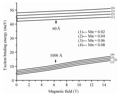
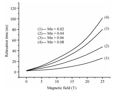
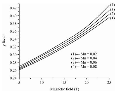
Hydrogenic acceptor binding energy as a function of dot radius in a GaMnAs/Ga0.6Al0.4As quantum dot is calculated including the exchange interaction of Mn alloy content with an itinerant carrier. Calculations are performed by varying its dot radius, for various Mn alloy contents in GaMnAs quantum dot within a single band effective mass approximation using variational method. The spin polaronic energy of the acceptor impurity for different Mn2+ is evaluated for different dot radii using a mean field theory in the presence of magnetic field strength. The magnetization is computed in the influence of magnetic field and the Mn ions. The effective g-factor of the valence band electron with the inclusion of effects of Mn ion impurities is found in the influence of the magnetic field. The exchange coupling constant is calculated for various magnetic field strengths. The results show that the p-d exchange interaction in the GaMnAs/Ga0.6Al0.4As quantum dot has a strong dependence on spatial confinement, effect of magnetic field strength and the Mn alloy content. Our results are in good agreement with the other investigators.


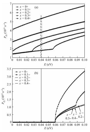
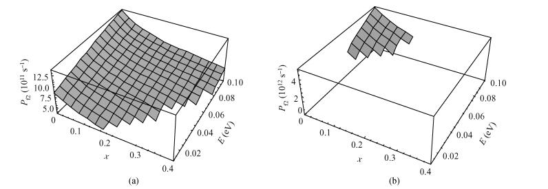
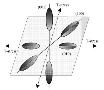
Inter valley scattering has a great impact on carrier mobility of strained Si materials, so based on Fermi's golden rule and the theory of Boltzmann collision term approximation, inter valley phonon scattering mechanism of electrons in nano scale strained Si (101) materials is established under the influence of both energy and stress. It shows that inter valley phonon f2, f3, g3 scattering rates decrease markedly in nano scale strained Si (101) materials with increasing stress. The quantized models can provide valuable references to the understanding of strained Si materials and the research on electron carrier mobility.


High pressure has a significant influence on β-FeSi2 band gaps and optical absorption tuning. In this work, using density functional theory, we investigate the effect of high pressure on the optical absorption behavior of a β-FeSi2 (100)/Si (001) interface with some Si vacancies. As the pressure increases, the optical absorption peak down-shifts firstly, reach minimum values, and then un-shifts slowly. The electronic orbital analysis indicates that the electronic transition between the highest occupied states and the lowest unoccupied states mainly originate from Fe atoms at the interface regions. Structural analysis discloses that the Si (001) slab partially offsets the pressure exerted on the β-FeSi2 (100) interface, but this effect will become weaker with further increasing pressure, and this physical mechanism plays an important role in its optical absorption behavior.


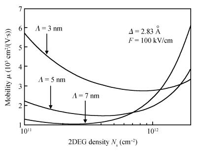
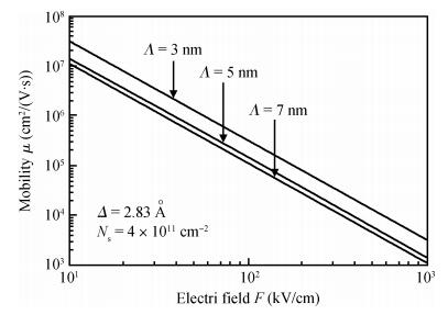
We have theoretically studied the mobility limited by interface roughness scattering on two-dimensional electrons gas (2DEG) at a single heterointerface (triangle-shaped quantum well). Our results indicate that, like the interface roughness scattering in a square quantum well, the roughness scattering at the AlxGa1-xAs/GaAs heterointerface can be characterized by parameters of roughness height Δ and lateral Λ, and in addition by electric field F. A comparison of two mobilities limited by the interface roughness scattering between the present result and a square well in the same condition is given.


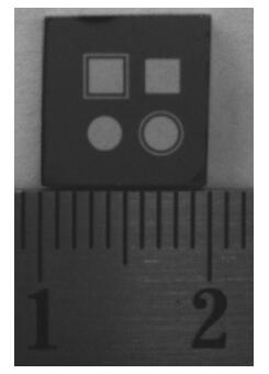
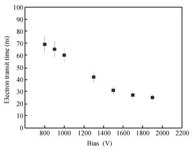
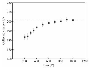
Charge transport characteristics of Cd0.95Mn0.05Te:In radiation detectors have been evaluated by combining time resolved current transient measurements with time of flight charge transient measurements. The shapes of the measured current pulses have been interpreted with respect to a concentration of net positive space-charge, which has resulted in an electric field gradient across the detector bulk. From the recorded current pulses the charge collection efficiency of the detector was found to approach 100%. From the evolution of the charge collection efficiency with applied bias, the electron mobility-lifetime product of μnτn=(8.5±0.4)×10-4 cm2/V has been estimated. The electron transit time was determined using both transient current technique and time of flight measurements in the bias range of 100-1900 V. From the dependence of drift velocity on applied electric field the electron mobility was found to be μn=(718±55) cm2/(V·s) at room temperature.


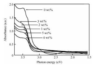
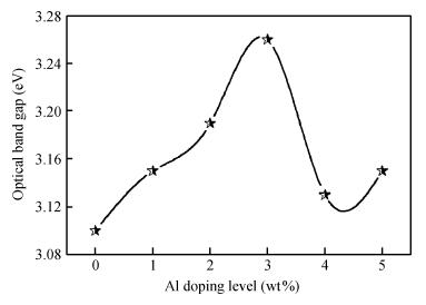
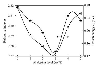
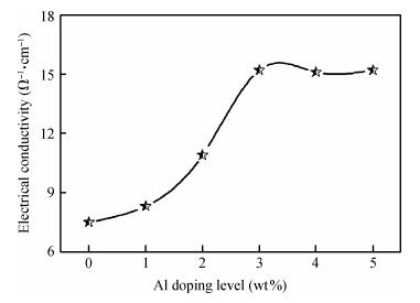
Transparent conductive Al doped ZnO thin films were deposited by ultrasonic spray technique. Conditions of preparation have been optimized to get good quality. A set of aluminum (Al) doped ZnO (between 0 and 5 wt%) thin films were grown on glass substrate at 350℃. Nanocrystalline films with a hexagonal wurtzite structure show a strong (002) preferred orientation. The maximum value of grain size G=32.05 nm is attained of Al doped ZnO film with 3 wt%. All the films have low absorbance in the visible region, thus the films are transparent in the visible region; the band gap energy increased from 3.10 to 3.26 eV when Al concentration increased from 0 to 3 wt%. The electrical conductivity of the films increased from 7.5 to 15.2 (Ω·cm)-1. So the best results are achieved in Al doped ZnO film with 3 wt%.


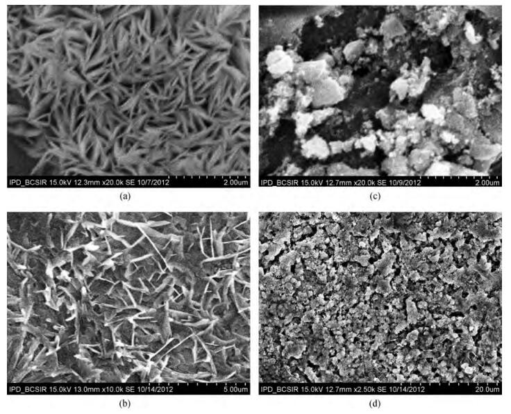
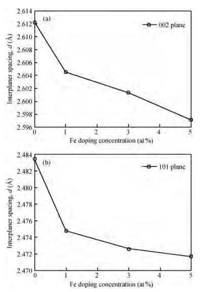
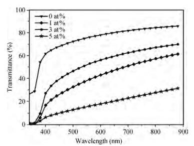
Fe-doped ZnO thin films have been prepared by spray pyrolysis on glass substrates and the influence of Fe-doping concentration on the structural and optical properties of the films has been studied. The X-ray diffraction (XRD) analysis shows that Fe doping has a significant effect on crystalline quality, grain size and strain in the thin films. The best crystalline structure is obtained for 3 at% Fe doping as observed from scanning electron microscopy (SEM) and XRD. However, lower or higher Fe-doping degrades the crystalline quality in turn. Moreover, UV spectroscopy demonstrates the influence of Fe-incorporation on visible range transmittance of ZnO where the best transmittance is obtained for 3 at% doping. The results have been illustrated simultaneously focusing previous results obtained from literature.


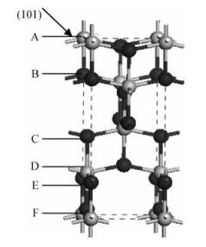
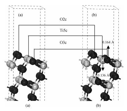
The TiO2 (101) surface was studied using the plane-wave ultrasoft pseudopotential method based on the density functional theory, with emphasis on the structure, surface energy, band structure, density of states, and charge population. The anatase TiO2 (101) crystal surface structure, whose outermost and second layers were terminated by twofold coordinated oxygen atoms and fivefold coordinated titanium atoms, was found to be much more stable. The surface energy of the 18-layer atoms model was 0.580 J/m2. The surface electronic structure was similar to that of the bulk and no surface state. Compared with the bulk structure, the band gap increased 0.36 eV, the Ti5c-O2c bond lengths reduced 0.171 Å after relaxation, and the charges of the surface were transferred to the body. Analysis of the optical properties of the TiO2 (101) surface showed that it did not absorb in the low-energy region. An absorption edge in the ultraviolet region corresponding to the energy of 3.06 eV was found.


Linearly graded InxGa1-xAs metamorphic buffers with different mismatch grading rates were grown on InP substrate by gas source molecular beam epitaxy. Room temperature photoluminescence spectra show that the sample with lower mismatch grading rate in the buffer has stronger photoluminescence signal, indicating the improved optical property. Atomic force microscope images show that the lower mismatch grading rate in the buffer leads to a slightly rougher surface. The relaxation procedure with two steps in the buffer layers has been observed by X-ray diffraction reciprocal space mapping. The measurements of X-ray diffraction also reveal that the lower mismatch grading rate in the buffer is beneficial for the lattice relaxation and release of residual strain. To further increase the relaxation degree, a lower mismatch grading rate and composition "overshoot" are suggested.


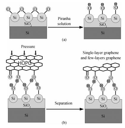
We develop a novel and convenient method to prepare large area single-layer and multi-layer graphene through surface modification with oxygen plasma. The obtained large area single-layer graphene is dozens of microns wide in the lateral dimension and characterized by optical microscopy, atomic force microscopy. Raman spectroscopy show multilayer graphene has less disorder density than single-layer graphene. X-ray photoelectron spectroscopy (XPS) analysis shows that hydroxyl groups are formed on the HOPG surface during oxygen plasma pre-treatment. Hydrogen bonds develop between hydroxyl groups on HOPG surface and silanol groups on hydroxylated SiO2/Si substrate, which facilitate the transfer process. This study may provide a potential approach to develop graphene-based devices by using the large area lithographic printing process.


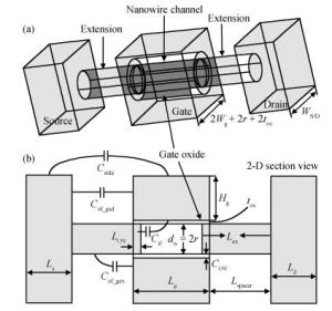
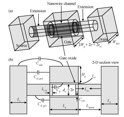
A physically based analytical model for surface potential and threshold voltage including the fringing gate capacitances in cylindrical surround gate (CSG) MOSFETs has been developed. Based on this a subthreshold drain current model has also been derived. This model first computes the charge induced in the drain/source region due to the fringing capacitances and considers an effective charge distribution in the cylindrically extended source/drain region for the development of a simple and compact model. The fringing gate capacitances taken into account are outer fringe capacitance, inner fringe capacitance, overlap capacitance, and sidewall capacitance. The model has been verified with the data extracted from 3D TCAD simulations of CSG MOSFETs and was found to be working satisfactorily.


Long and well-aligned ZnO nanowires were hydrothermally synthesized on FTO glass based on a ZnO seed layer which was prepared by spin-coating and annealing techniques. The effect of the growth solution refreshment on the morphology of ZnO nanowires was investigated and the possible mechanism was discussed. After refreshing the growth solution for 5 cycles, ZnO nanowires of 120 nm in diameter and 20 μm in length were obtained. The prepared ZnO nanowires were used as photoelectrodes in dye-sensitized solar cells (DSSCs), showing excellent photovoltaic performance. With the increase of growth cycles of ZnO nanowires, the photocurrent of DSSCs increased obviously due to the increased dye loading on the surface of ZnO nanowires. The results indicated that the long and well-aligned ZnO nanowires are promising for DSSCs application.


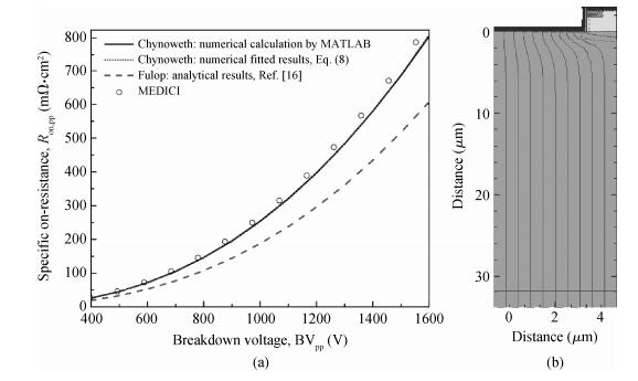
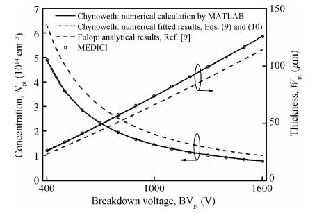
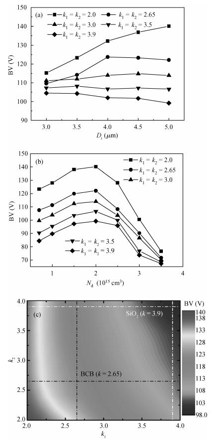
The relations among the breakdown voltage, the width and the concentration of the voltage-sustaining layer for the non-punch-through (NPT) and punch-through (PT) abrupt parallel-plane junctions have been re-established based on the ionization integral by the Chynoweth model, distinguished from the conventional results obtained by the Fulop model. The numerical calculation results indicate that the new expressions are more accurate than those in previous literature. While the breakdown voltage of the NPT case varied from 400 to 1600 V using the Chynoweth model, the value using the Fulop model is overestimated by 12% (478 V) to 18% (1895 V). For the PT case with optimum design of the specific on-resistance, when the breakdown voltage is varied from 400 to 1600 V, the width and concentration are from 81.0168% to 80.2416% and from 91.4341% to 91.6941% of those of the NPT cases, respectively. The relations between the specific on-resistance and the breakdown voltage for both the NPT and PT structures are also established. Simulation results by MEDICI show good agreement with the proposed expressions.


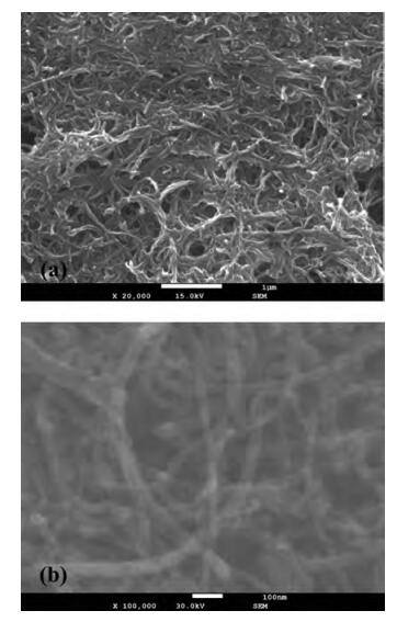
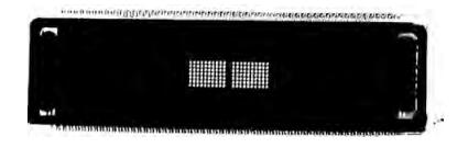
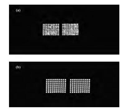
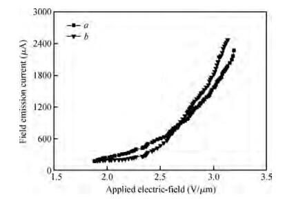
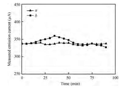
Based on an effective screen-printing process, a novel sandwich layered cathode electrode was developed on a cathode faceplate. The ZnO electrode was sandwiched between an indium tin oxide (ITO) electrode layer and a silver electrode layer, and the carbon nanotube was prepared directly on the exposed ITO electrode layer surface. The cathode potential could be conducted to the carbon nanotube with the sandwich layered cathode electrode. Using the carbon nanotube as a field emitter, a triode field emission display prototype with a sandwich layered cathode electrode was fabricated, which possessed a better field emission characteristic, higher luminous brightness and better emission image luminance uniformity. The turn-on electric field was 1.88 V/μm and the measured maximum field emission current was 2273.6 μA at 3.19 V/μm. By the method of adjusting the field emission current, the electron-emitting uniform capacity of the carbon nanotube cold cathode could be modified, and the emission image luminance uniformity and the emission current stability of triode field emission display prototype was also be improved significantly. The emission current fluctuation of the sandwich layered cathode electrode type field emission display was less than 1.1%. Furthermore, the total manufacture cost of the triode field emission display prototype was low.


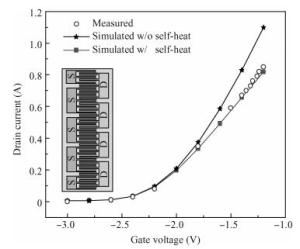
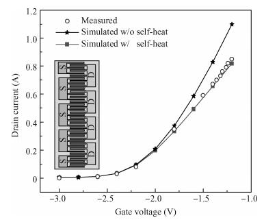
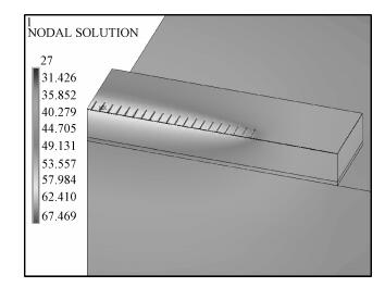
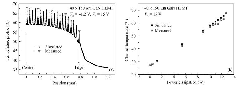
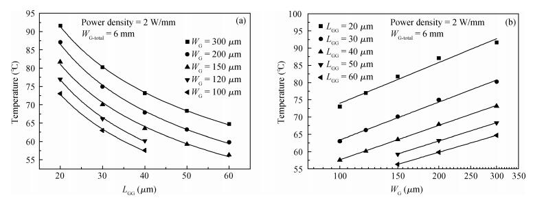
Self-heating in multi-finger AlGaN/GaN high-electron-mobility transistors (HEMTs) is investigated by measurements and modeling of device junction temperature under steady-state operation. Measurements are carried out using micro-Raman scattering to obtain the detailed and accurate temperature distribution of the device. The device peak temperature corresponds to the high field region at the drain side of gate edge. The channel temperature of the device is modeled using a combined electro-thermal model considering 2DEG transport characteristics and the Joule heating power distribution. The results reveal excellent correlation to the micro-Raman measurements, validating our model for the design of better cooled structures. Furthermore, the influence of layout design on the channel temperature of multi-finger AlGaN/GaN HEMTs is studied using the proposed electro-thermal model, allowing for device optimization.


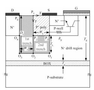
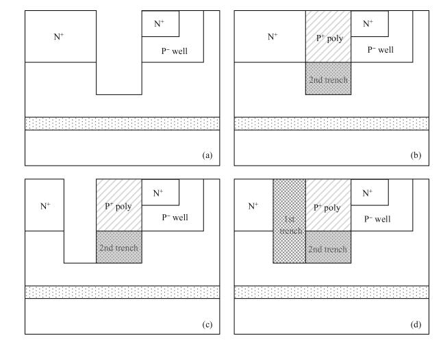
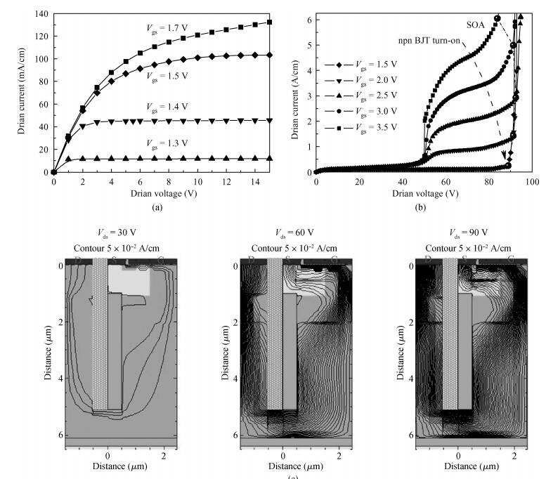
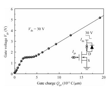
A novel silicon-on-insulator (SOI) MOSFET with a variable low-k dielectric trench (LDT MOSFET) is proposed and its performance and characteristics are investigated. The trench in the drift region between drain and source is filled with low-k dielectric to extend the effective drift region. At OFF state, the low-k dielectric trench (LDT) can sustain high voltage and enhance the dielectric field due to the accumulation of ionized charges. At the same time, the vertical dielectric field in the buried oxide can also be enhanced by these ionized charges. Additionally, ON-state analysis of LDT MOSFET demonstrates excellent forward characteristics, such as low gate-to-drain charge density ( < 0.6 nC/mm2) and a robust safe operating area (0-84 V).


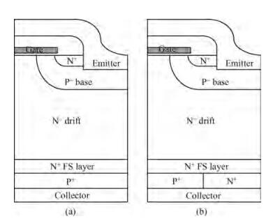
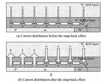
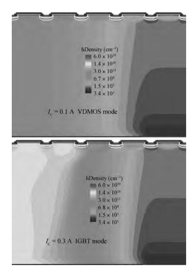
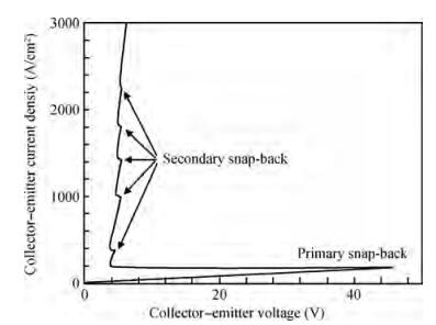
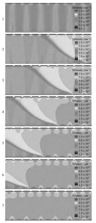
The RC-IGBT (reverse conducting insulated gate bipolar transistor) is a new kind of power semiconductor device which has many advantages such as smaller chip size, higher power density, lower manufacturing cost, softer turn off behavior, and better reliability. However, its performance has a number of drawbacks, such as the snap-back effect. In this paper, an introduction about the snap-back effect of the RC-IGBT is given firstly. Then the physical explanations are presented with two simplified models. After that, some numerical simulations are carried out to verify the correctness of the models.


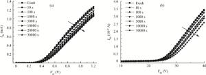
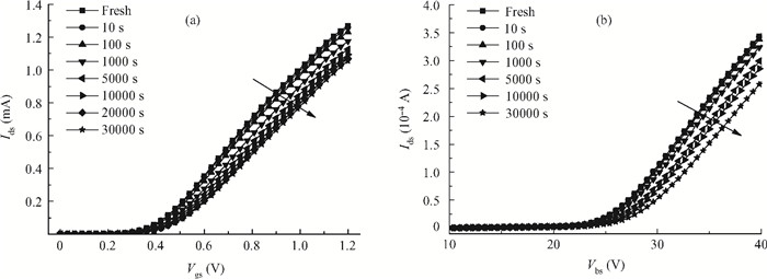
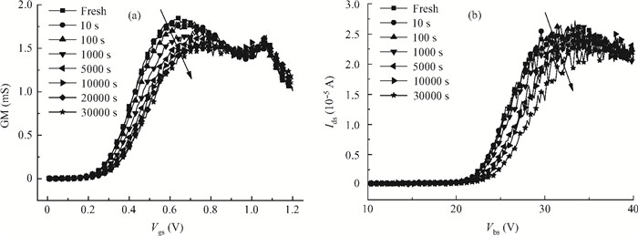
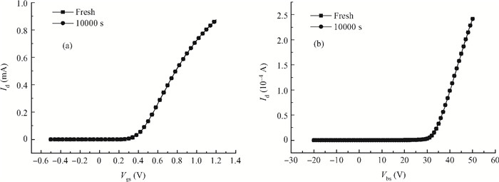
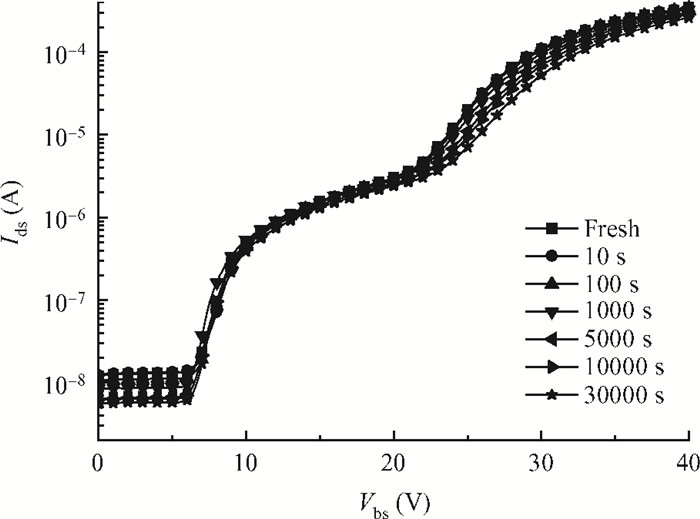
The hot-carrier effect characteristic in a deep submicron partially depleted SOI NMOSFET is investigated. Obvious hot-carrier degradation is observed under off-state stress. The hot-carrier damage is supposed to be induced by the parasitic bipolar effects of a float SOI device. The back channel also suffers degradation from the hot carrier in the drain depletion region as well as the front channel. At low gate voltage, there is a hump in the sub-threshold curve of the back gate transistor, and it does not shift in the same way as the main transistor under stress. While under the same condition, there is a more severe hot-carrier effect with a shorter channel transistor. The reasons for those phenomena are discussed in detail.


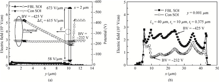
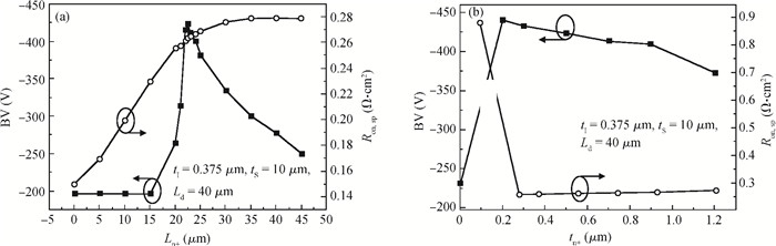
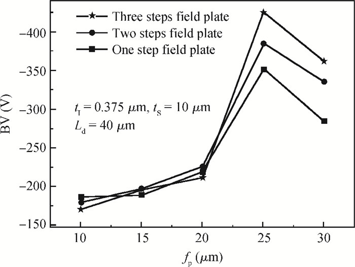
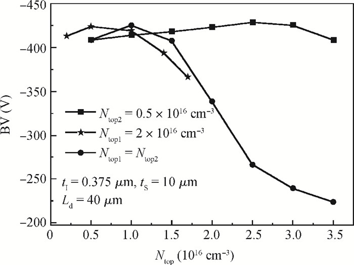
A novel silicon-on-insulator (SOI) high-voltage pLDMOS is presented with a partial interface equipotential floating buried layer (FBL) and its analytical model is analyzed in this paper. The surface heavily doped p-top layers, interface floating buried N+/P+ layers, and three-step field plates are designed carefully in the FBL SOI pLDMOS to optimize the electric field distribution of the drift region and reduce the specific resistance. On the condition of ESIMOX (epoxy separated by implanted oxygen), it has been shown that the breakdown voltage of the FBL SOI pLDMOS is increased from-232 V of the conventional SOI to-425 V and the specific resistance Ron, sp is reduced from 0.88 to 0.2424 Ω·cm2.


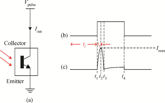
This paper proposed a discrete operation mode for a punchthrough (PT) phototransistor, which is suitable for low power application, since the bias current is only necessary during the read-out phase. Moreover, simulation results show that with the new operation mode, the photocurrent is much larger than that of continuous operation mode. An ultra-high responsivity of 2×10⁷A/W at 10-9 W/cm2 is obtained with a small detector size of 1 μm2. In CMOS image sensor applications, with an integration time of 10 ms, a normalized pixel responsivity of 220 V·m2/W·s·μm2 is obtained without any auxiliary amplifier.


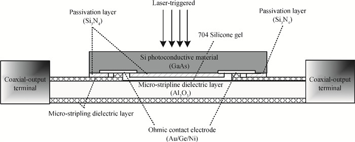
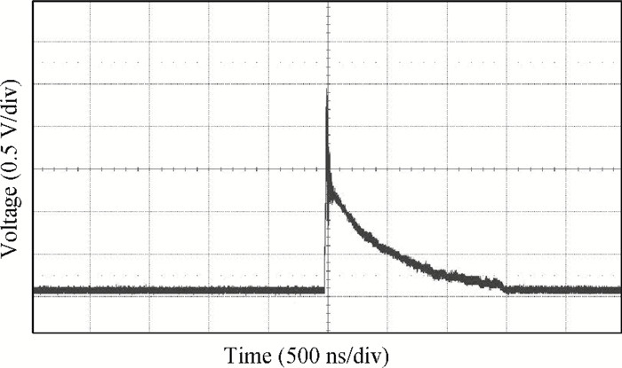
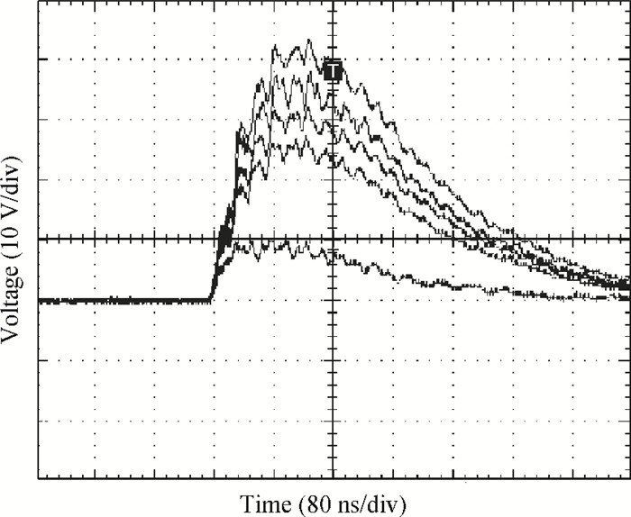
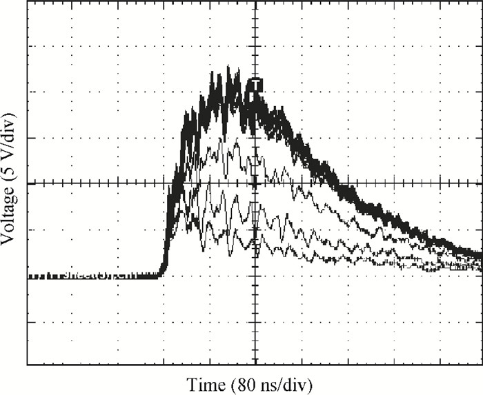
Experiments with the limited space-charge accumulation (LSA) mode of oscillation in a large gap semi-insulating (SI) GaAs photoconductive semiconductor switch (PCSS) are discussed. It has been observed that growth and drift of a photo-activated charge domain (PACD) are quenched only when the bias voltage is more than twice the threshold voltage. The original negative resistance characteristics are directly utilized in the LSA mode; during LSA operation the spatial average of the electric field varies over a large portion of the negative differential mobility region of the velocity-electric field characteristic. The work efficiency of an SI GaAs PCSS is remarkably enhanced by electric field excursions into the positive resistance region when the total electric field is only below the threshold part of the time. The LSA mode can only operate in the certain conditions that satisfy the quenching of the accumulation layer and the smaller initial domain voltage.


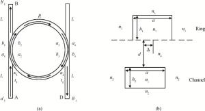
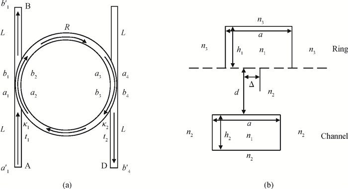
By using the coupled mode theory and the transfer matrix technique, the optical transfer function is presented for analyzing the size of the waveguide, radius of the microring, free spectral range and amplitude coupling ratio of the vertical coupling microring resonator. Under the central wavelength of 1550 nm, optimization and simulation are performed when the central deviation between the ring and the channel is 0, 0.5, 1 μm, respectively, the 3-dB bandwidth of the spectral response is about 0.21, 0.09, 0.03 nm, and the intensity of the nonresonant light is below-30, -40, -50 dB, respectively.


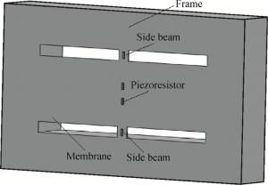
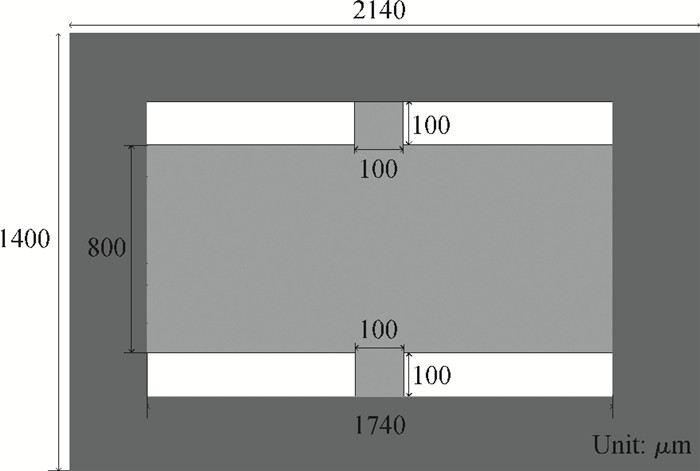
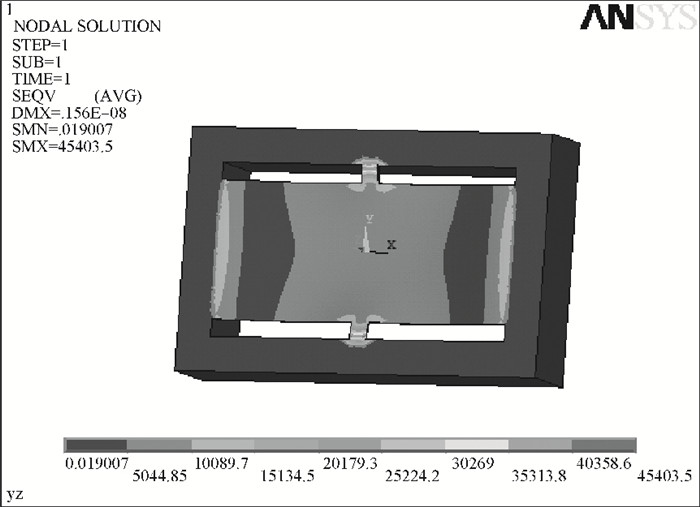
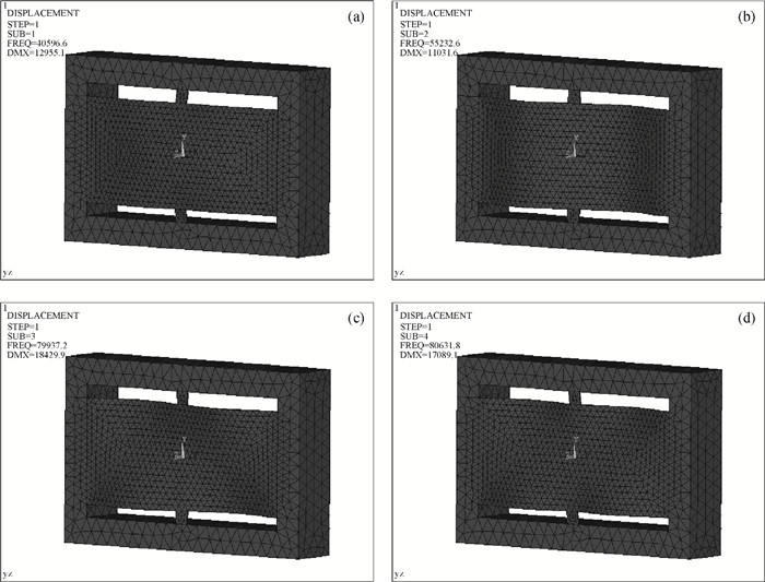
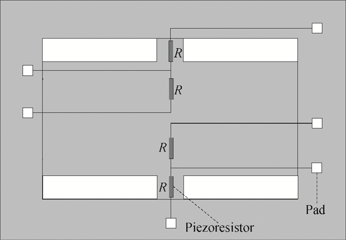
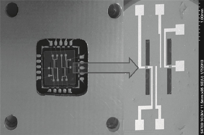
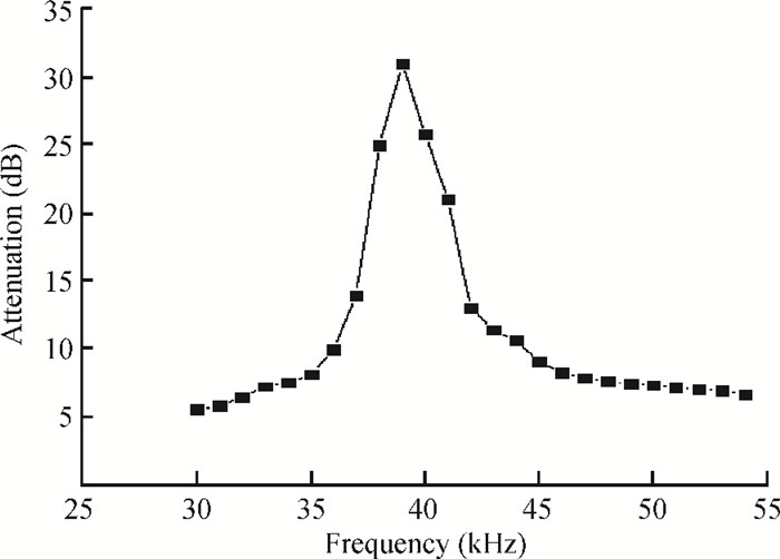
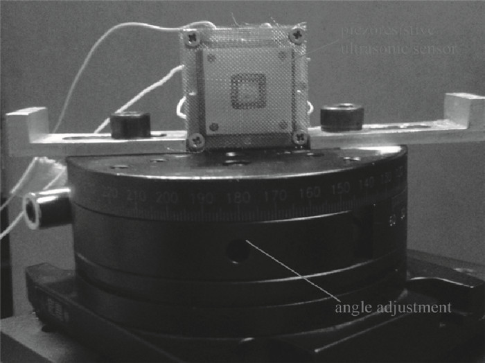
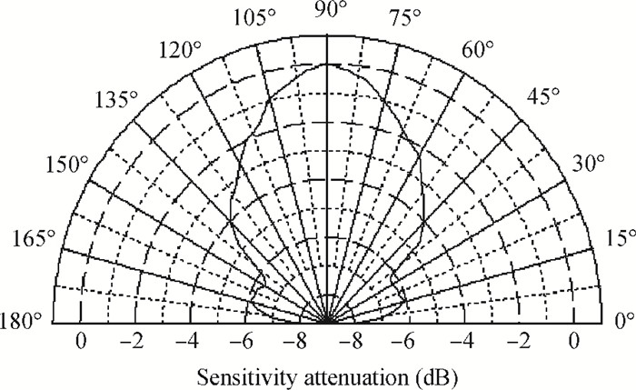
A kind of piezoresistive ultrasonic sensor based on MEMS is proposed, which is composed of a membrane and two side beams. A simplified mathematical model has been established to analyze the mechanical properties of the sensor. On the basis of the theoretical analysis, the structural size and layout location of the piezoresistors are determined by simulation analysis. The boron-implanted piezoresistors located on membrane and side beams form a Wheatstone bridge to detect acoustic signal. The membrane-beam microstructure is fabricated integrally by MEMS manufacturing technology. Finally, this paper presents the experimental characterization of the ultrasonic sensor, validating the theoretical model used and the simulated model. The sensitivity reaches-116.2 dB (0 dB reference=1 V/μbar, 31 kHz), resonant frequency is 39.6 kHz, direction angle is 55°.


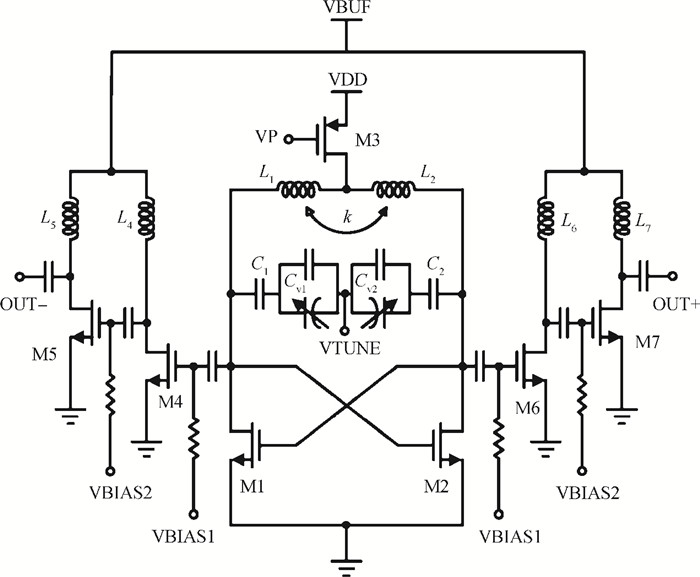
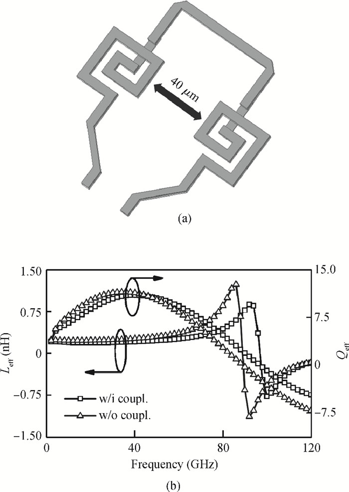
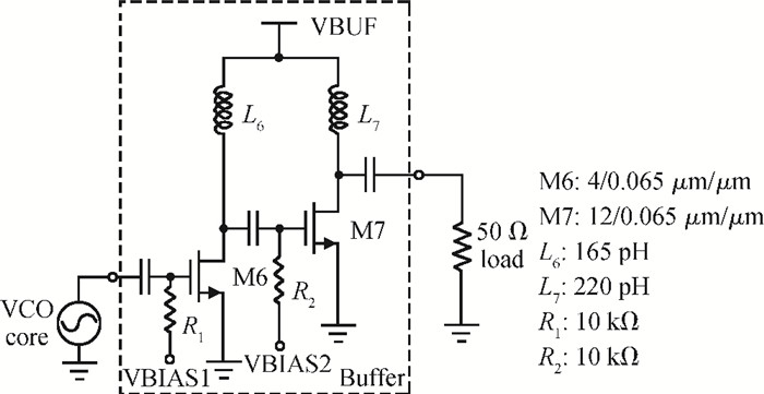
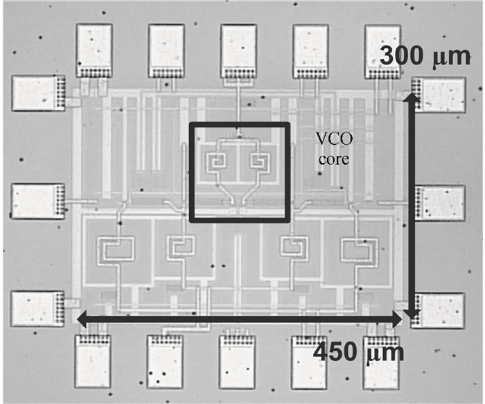
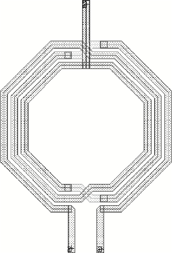
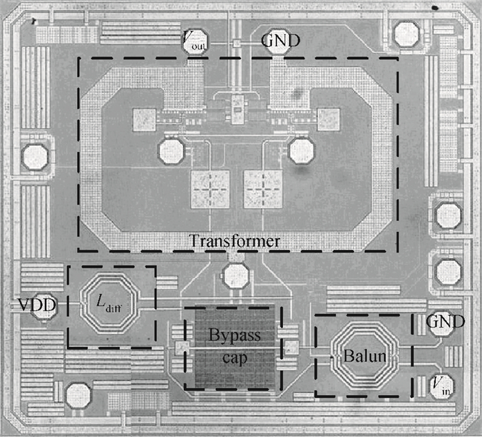
A 50 GHz cross-coupled voltage controlled oscillator (VCO) considering the coupling effect of inductors based on a 65 nm standard complementary metal oxide semiconductor (CMOS) technology is reported. A pair of inductors has been fabricated, measured and analyzed to characterize the coupling effects of adjacent inductors. The results are then implemented to accurately evaluate the VCO's LC tank. By optimizing the tank voltage swing and the buffer's operation region, the VCO achieves a maximum efficiency of 11.4% by generating an average output power of 2.5 dBm while only consuming 19.7 mW (including buffers). The VCO exhibits a phase noise of-87 dBc/Hz at 1 MHz offset, leading to a figure of merit (FoM) of-167.5 dB/Hz and a tuning range of 3.8% (from 48.98 to 50.88 GHz).


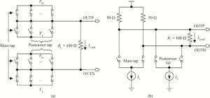
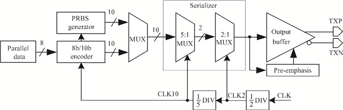
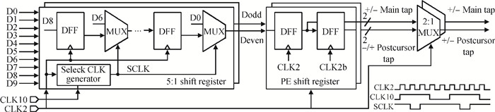
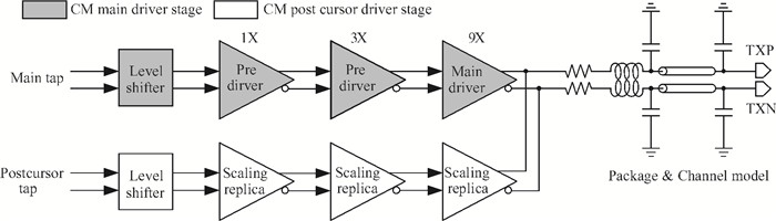
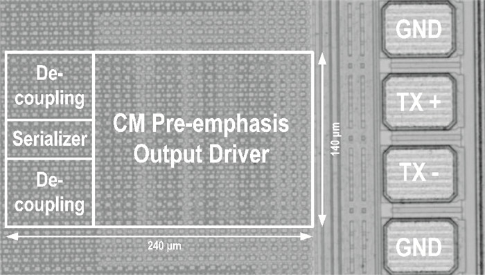
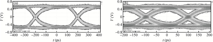
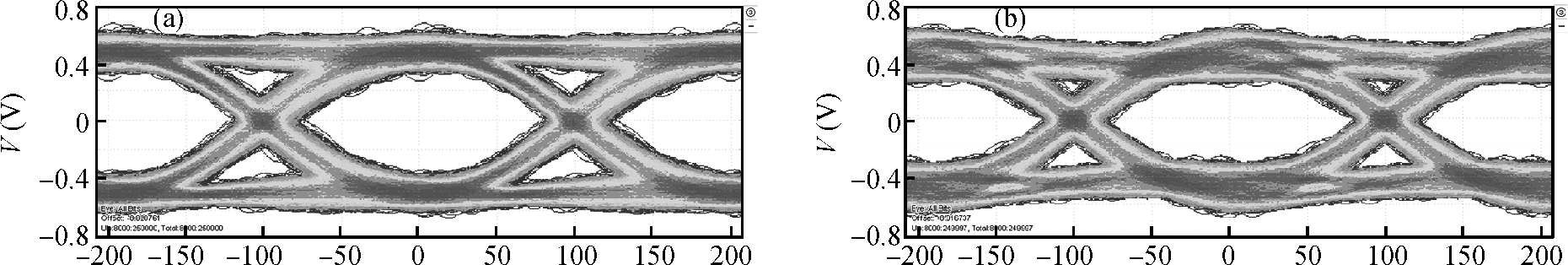
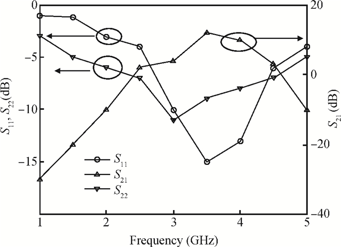
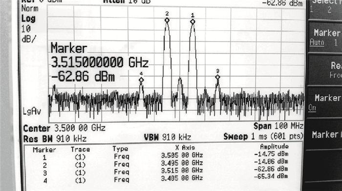
A multi-standard compatible transmitter with pre-emphasis for high speed serial links is presented. Based on the comparison between voltage mode (VM) and current mode (CM) output driver architectures, a low power CM output driver with reverse scaling and bias current filtering technique is proposed. A 2-tap pre-emphasis filter is used to reduce the intersymbol interference caused by the low-pass channel, and a high speed, low power combined serializer is implemented to convert 10 bit parallel data into a serial data stream. The whole transmitter is fabricated in 65 nm 1.2 V/2.5 V CMOS technology. It provides an eye height greater than 800 mV for data rates of both 2.5 Gb/s and 5 Gb/s. The output root mean square jitter of the transmitter at 5 Gb/s is only 9.94 ps without pre-emphasis. The transmitter consumes 41.2 mA at 5 Gb/s and occupies only 240×140 μm2.


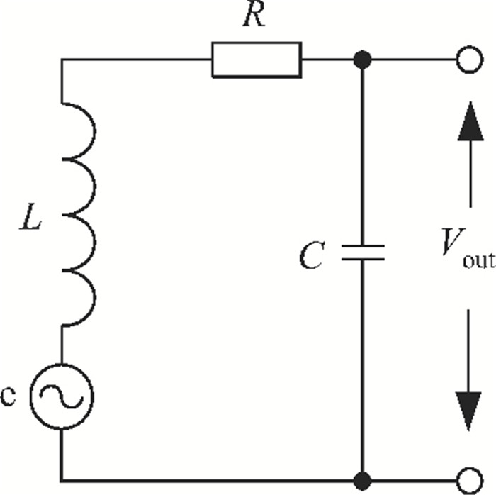
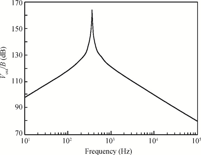
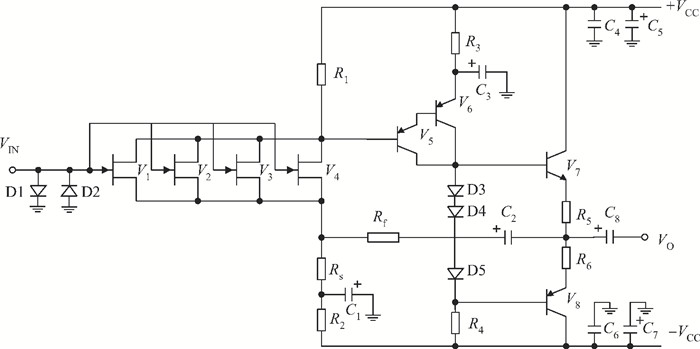
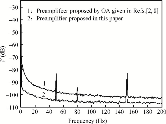
Besides the electrode-pair antenna, the magnetic antenna is also used for the extremely low frequency (ELF) submarine communication. To receive the weak ELF signals, the structure of a small sized magnetic antenna determines its specific electrical characteristics. The ELF magnetic antenna shows high internal resistance, alternating-current impedance, and a resonance frequency near the operating bandwidth. In accordance with the electrical characteristics of ELF magnetic antenna, a low noise preamplifier and frequency compensation circuit were designed and realized. The preamplifier is a three-stage negative feedback circuit, which is composed of parallel JFET, common-emitter amplifier with a Darlington structure and a common-collector amplifier in push-pull connection. And a frequency compensation circuit is cascaded to compensate the characteristic in low frequency range. In the operating bandwidth f=30-200 Hz, the circuit has a gain of 39.4 dB. The equivalent input noise is 1.97 nV/$\sqrt {{\text{Hz}}} $ and the frequency response keeps flat in operating bandwidth. The proposed preamplifier of the ELF magnetic antenna performs well in receiving ELF signals.


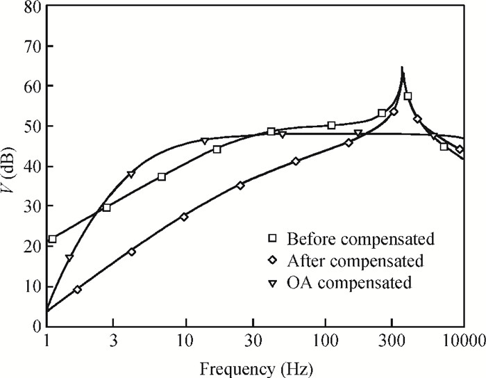
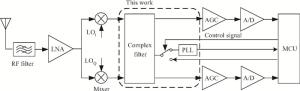
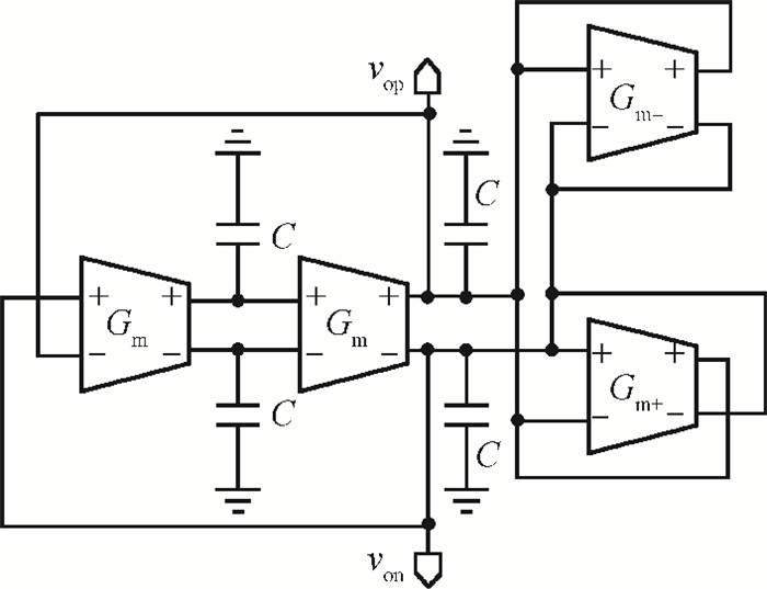
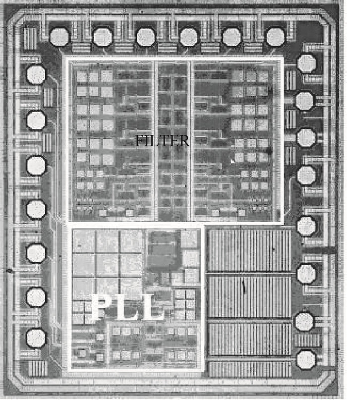
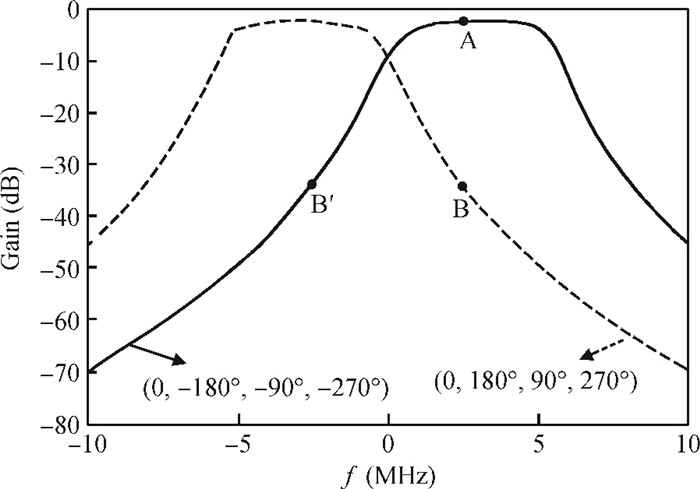
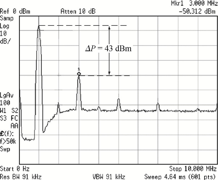
This paper presents a reconfigurable fifth-order complex Gm-C filter for different data rates in low-IF WiMAX applications. The design procedure and linearized measures to realize the complex filter are described. In order to achieve the reconfigurability of bandwidth window, the center frequency and the cutoff frequency filter are adjusted simultaneously by changing capacitor values while keeping transconductors unchanged. Also, the filter integrates an on-chip automatic frequency tuning circuit based on a PLL. Experimental results show that it has an IRR of 32 dB, a THD of-43 dB, and an input-referred noise of 21 μVrms. The chip is fabricated in 0.13 μm CMOS process, occupies 0.7×1 mm2, and consumes 4.8 mA current from a 1.2 V power supply.


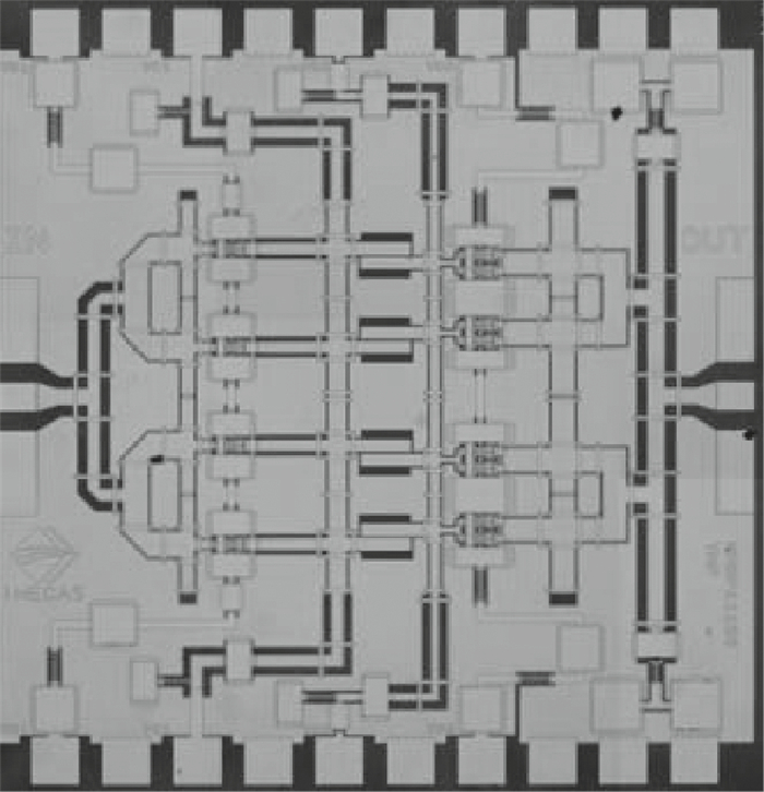
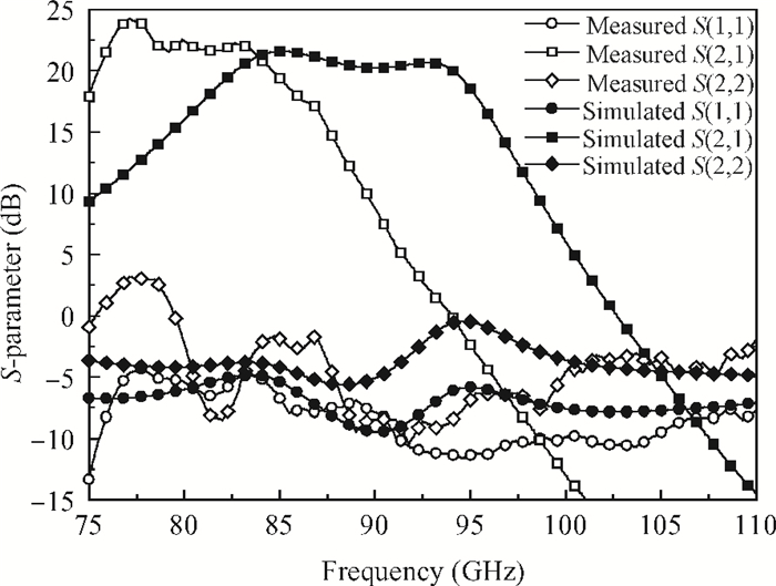
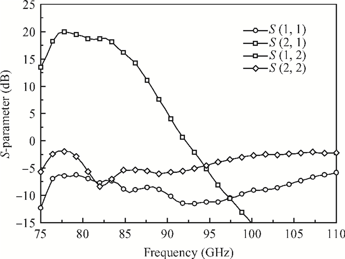
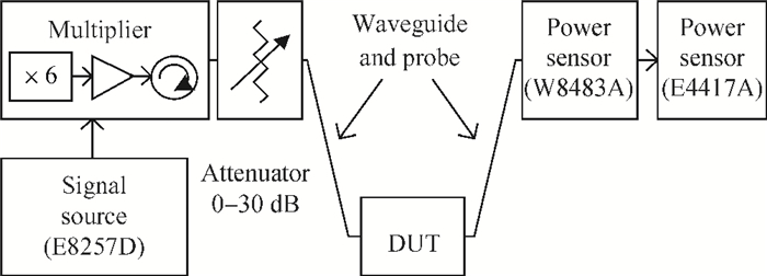
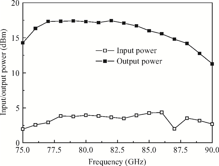
A two-stage MMIC power amplifier has been realized by use of a 1-μm InP double heterojunction bipolar transistor (DHBT). The cascode structure, low-loss matching networks, and low-parasite cell units enhance the power gain. The optimum load impedance is determined from load-pull simulation. A coplanar waveguide transmission line is adopted for its ease of fabrication. The chip size is 1.5$ \times $1.7 mm2 with the emitter area of 16$ \times $1 μm$ \times $15 μm in the output stage. Measurements show that small signal gain is more than 20 dB over 75.5-84.5 GHz and the saturated power is 16.9 dBm @ 79 GHz with gain of 15.2 dB. The high power gain makes it very suitable for medium power amplification.


A fully integrated CMOS differential power amplifier driver (PAD) is proposed for WiMAX applications. In order to fulfill the differential application requirements, a transmission line transformer is used as the output matching network. A differential inductance constitutes an inter-stage matching network. Meanwhile, an on chip balun realizes input matching as well as single-end to differential conversion. The PAD is fabricated in a 0.13 μm RFCMOS process. The chip size is 1.1×1.1 mm2 with all of the matching network integrated on chip. The saturated power is around 10 dBm and power gain is about 12 dB.


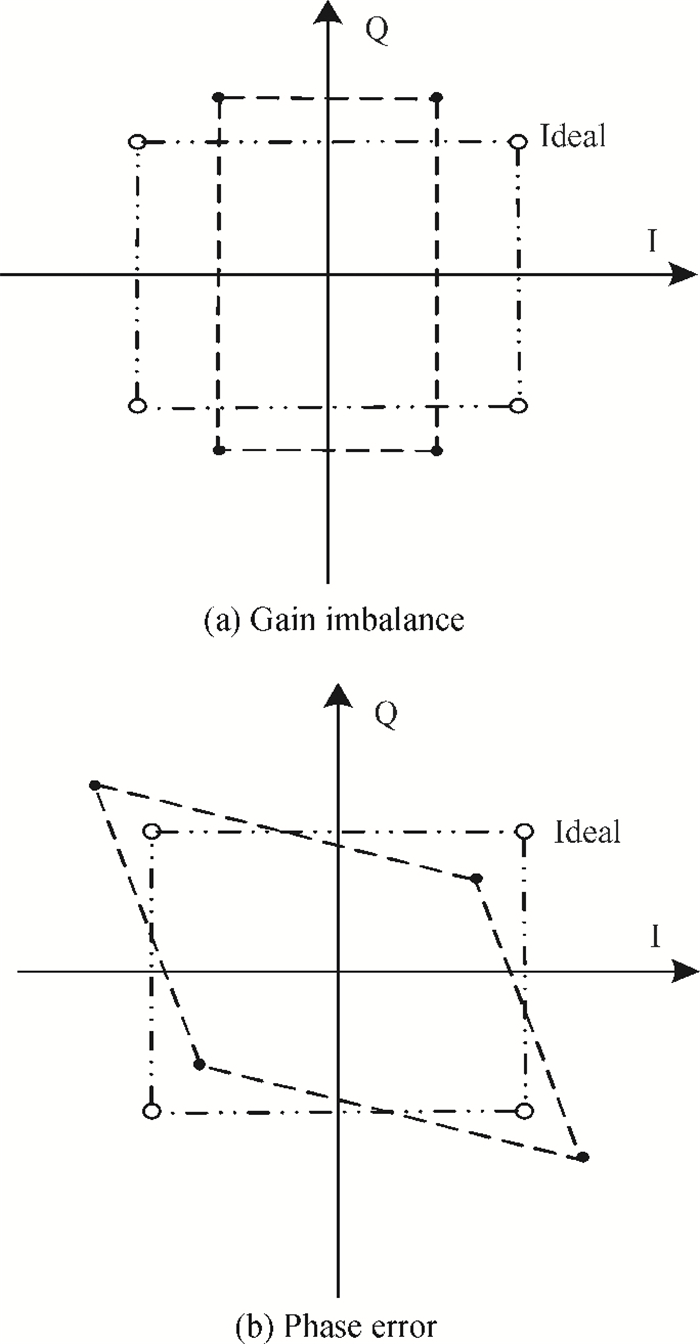
A novel I/Q mismatch calibration technique based on a digital baseband for a direct conversion transmitter is implemented in TSMC 0.13 μm CMOS technology. The proposed technique finishes a calibration task, which only needs a calibration chain to detect mismatches and then transmit them to the digital baseband. Simulation results show that the calibrated errors of the proposed technique are less than 7%. The measurement results indicate the function of the proposed technique is correct, but the performance should be improved further.


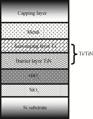
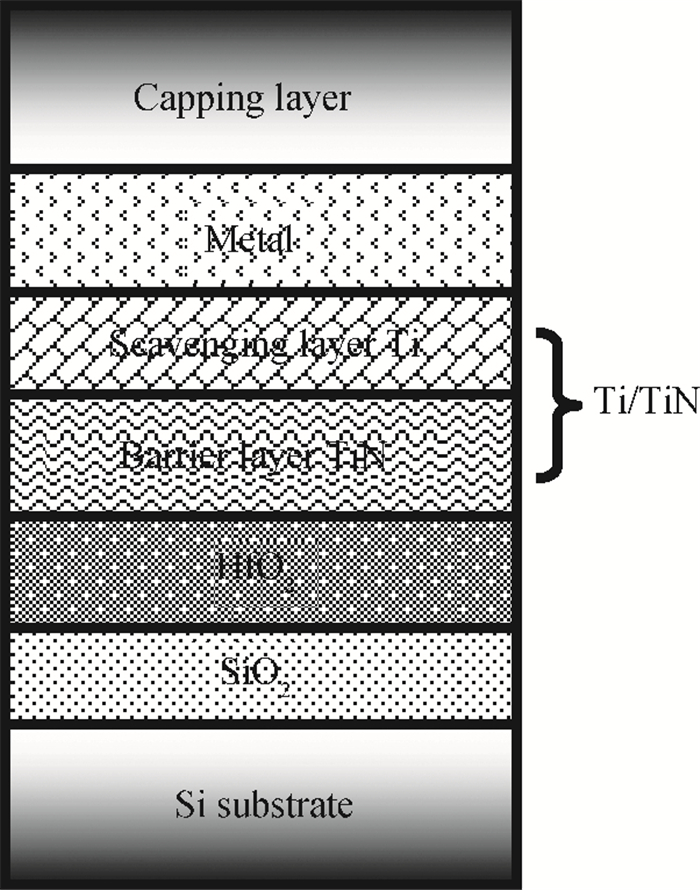
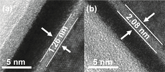
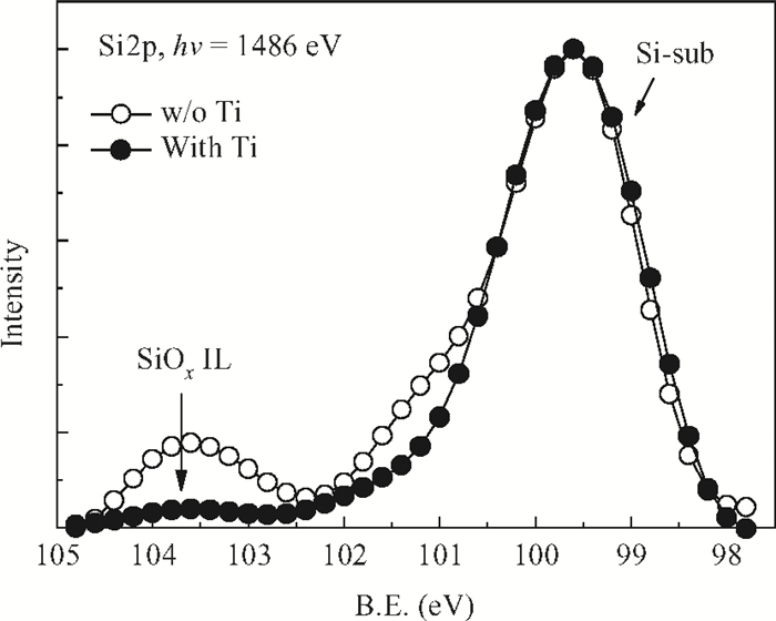
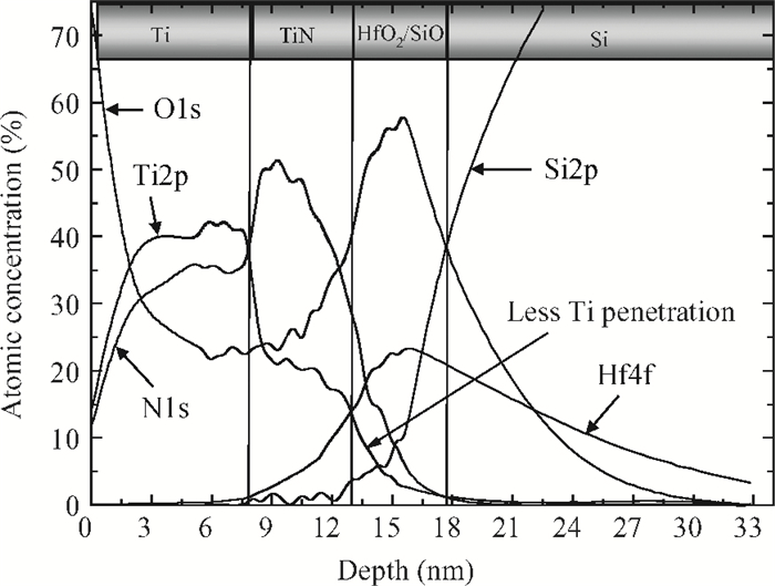
High permittivity materials have been required to replace traditional SiO2 as the gate dielectric to extend Moore's law. However, growth of a thin SiO2-like interfacial layer (IL) is almost unavoidable during the deposition or subsequent high temperature annealing. This limits the scaling benefits of incorporating high-k dielectrics into transistors. In this work, a promising approach, in which an O-scavenging metal layer and a barrier layer preventing scavenged metal diffusing into the high-k gate dielectric are used to engineer the thickness of the IL, is reported. Using a Ti scavenging layer and TiN barrier layer on a HfO2 dielectric, the effective removal of the IL and almost no Ti diffusing into the HfO2 have been confirmed by high resolution transmission electron microscopy and X-ray photoelectron spectroscopy.


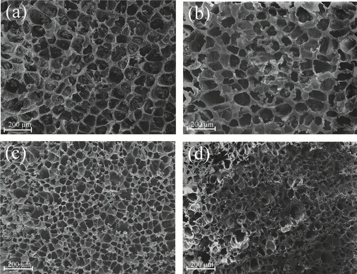
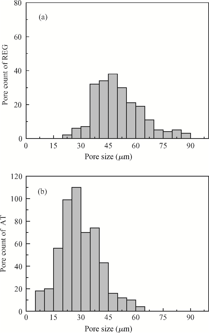
Chemical mechanical planarization (CMP) of amorphous Ge2Sb2Te5 (a-GST) is investigated using two typical soft pads (politex REG and AT) in acidic slurry. After CMP, it is found that the removal rate (RR) of a-GST increases with an increase of runs number for both pads. However, it achieves the higher RR and better surface quality of a-GST for an AT pad. The in-situ sheet resistance (Rs) measure shows the higher Rs of a-GST polishing can be gained after CMP using both pads and the high Rs is beneficial to lower the reset current for the PCM cells. In order to find the root cause of the different RR of a-GST polishing with different pads, the surface morphology and characteristics of both new and used pads are analyzed, it shows that the AT pad has smaller porosity size and more pore counts than that of the REG pad, and thus the AT pad can transport more fresh slurry to the reaction interface between the pad and a-GST, which results in the high RR of a-GST due to enhanced chemical reaction.


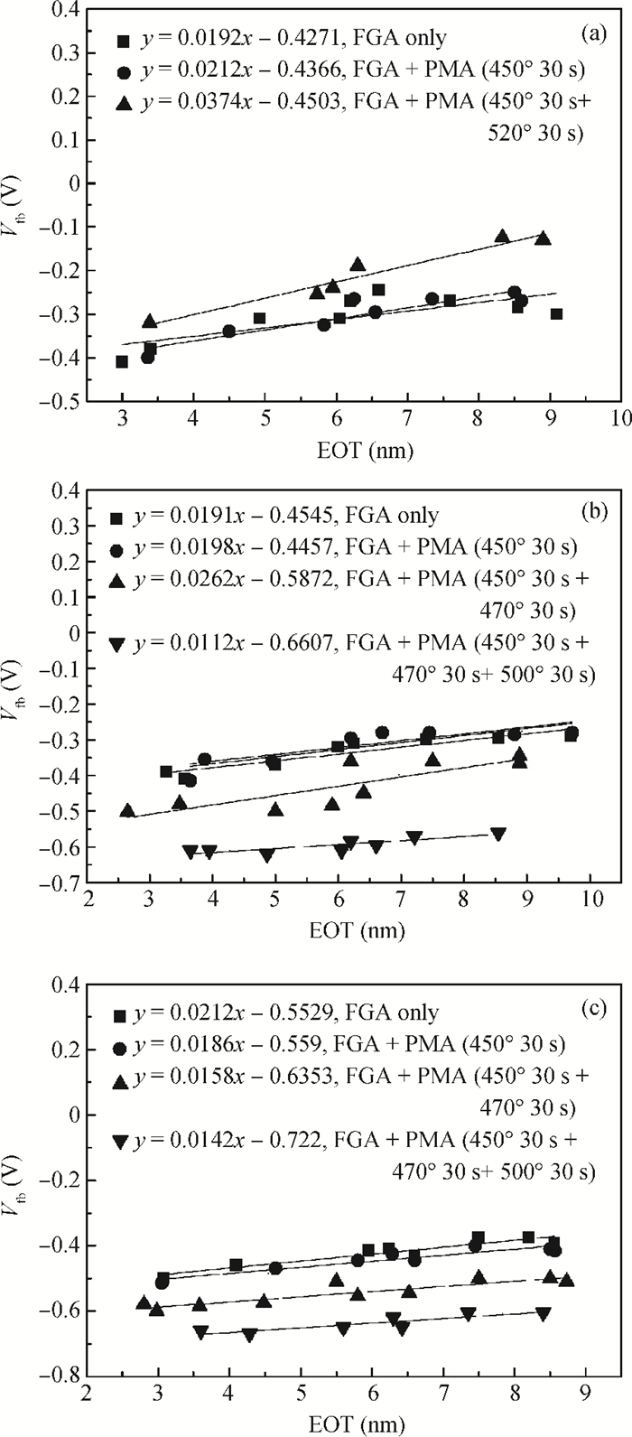
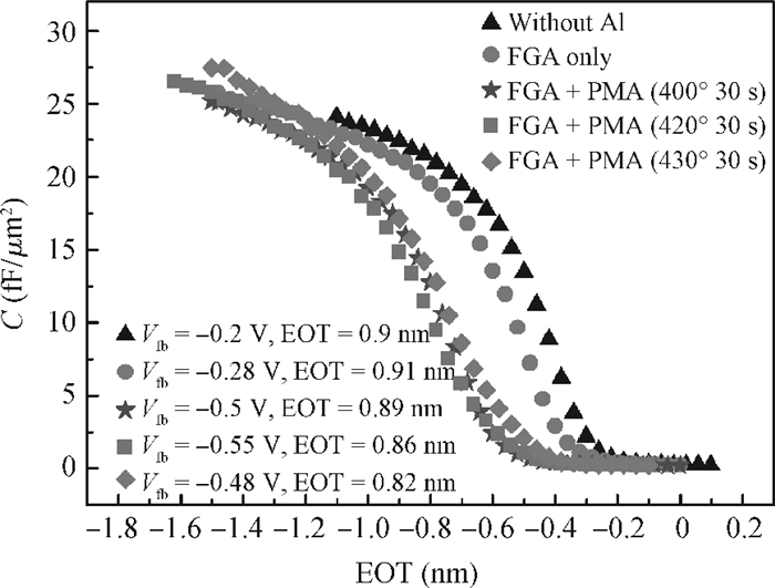
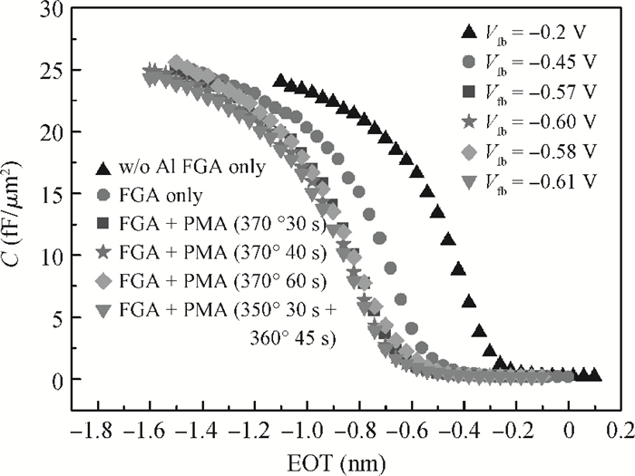
The effect of Al incorporation on the effective work function (EWF) of TiN metal gate was systematically investigated. Metal-oxide-semiconductor (MOS) capacitors with W/TiN/Al/TiN gate stacks were used to fulfill this purpose. Different thickness ratios of Al to TiN and different post metal annealing (PMA) conditions were employed. Significant shift of work function towards to Si conduction band was observed, which was suitable for NMOS and the magnitude of shift depends on the processing conditions.