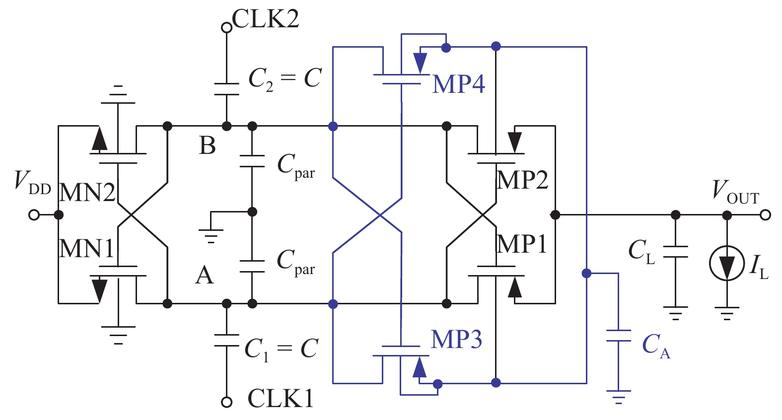
Fig. 1.
Conventional cross-coupled voltage doubler.
SEMICONDUCTOR INTEGRATED CIRCUITS
Jie Zhang, Hong Zhang and Ruizhi Zhang
Corresponding author: Hong Zhang, Email: hongzhang@xjtu.edu.cn
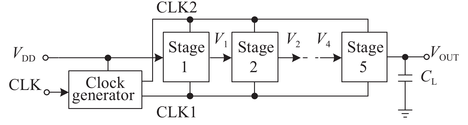
Abstract: This paper presents a high-efficiency charge pump circuit composed of cascaded cross-coupled voltage doublers implemented in an isolated bipolar-CMOS-DMOS (BCD) technology for implantable medical devices. Taking advantage of the transistor structures in the isolated BCD process, the leakage currents caused by the parasitic PNP transistors in the cross-coupled PMOS serial switches are eliminated by simply connecting the inside substrate terminal to the isolation terminal of each PMOS transistor. The simple circuit structure leads to small parasitic capacitance in the voltage doubler, which in turn ensures high efficiency of the overall charge pump. The proposed charge pump with 5 cascaded voltage doublers is fabricated in a 0.35-μm isolated BCD process. Measurement results with 2-V power supply, 1-MHz driving clock frequency and 40-μA current load show that an efficiency of 72.6% is achieved, and the output voltage can be pumped to about 11.5 V at zero load current. The chip area of the charge pump is 1.6 × 0.35 mm2.
Key words: voltage doubler, charge pump, high-efficiency, implantable medical device
| [1] |
Nagaraj S, Rassam F G. Improved noncoherent UWB receiver for implantable biomedical devices. IEEE Trans Biomed Eng, 2016, 63(10): 2220 doi: 10.1109/TBME.2015.2511538
|
| [2] |
Zhou J, Kim A, Ziaie B. An ultrasonically controlled power management system for implantable biomedical devices. IEEE Biomed Circuits Syst Conf, 2015: 1
|
| [3] |
Lee S Y, Hong J H, Hsieh C H, et al. A Low-power 13.56 MHz RF front-end circuit for implantable biomedical devices. IEEE Trans Biomed Circuits Syst, 2013, 7(3): 256 doi: 10.1109/TBCAS.2012.2212276
|
| [4] |
Wong L S Y, Hossain S, Ta A, et al. A very low-power CMOS mixed-signal IC for implantable pacemaker applications. IEEE J Solid-State Circuits, 2004, 39(12): 2446 doi: 10.1109/JSSC.2004.837027
|
| [5] |
Zhang J, Zhang H, Zhang R, et al. A mixed-signal ASIC for triple-chamber cardiac pacemakers with heart resistance measurement. IEEE Asian Solid-State Circuits Conference, 2015: 1
|
| [6] |
Yip M, Jin R, Nakajima H H, et al. A fully-implantable cochlear implant SoC with piezoelectric middle-ear sensor and arbitrary waveform neural stimulation. IEEE J Solid-State Circuits, 2015, 50(1): 214 doi: 10.1109/JSSC.2014.2355822
|
| [7] |
Azin M, Guggenmos D J, Barbay S, et al. A battery-powered activity-dependent intracortical microstimulation IC for brain-machine-brain Interface. IEEE J Solid-State Circuits, 2011, 46(4): 731 doi: 10.1109/JSSC.2011.2108770
|
| [8] |
Novo A, Gerosa A, Neviani A, et al. Programmable voltage multiplier for pacemaker output pulse generation. Electron Lett, 1999, 35(7): 560 doi: 10.1049/el:19990369
|
| [9] |
Novo A, Gerosa A, Neviani A, et al. A CMOS 0.8 μm programmable charge pump for the output stage of an implantable pacemaker. IEEE International Caracas Conference on Devices, Circuits and Systems, 2000: 34/1
|
| [10] |
Gak J, Miguez M, Arnaud A. A programmable charge pump voltage converter for implantable medical devices in a HV technology. IEEE Latin American Symposium on Circuits and Systems, 2013: 1
|
| [11] |
Esmailiyan A, Shaker A, Ghotbi I, et al. A charge-pump based multi-mode stimuli generator for cardiac pacemaking. IEEE International New Circuits and Systems Conference, 2016: 1
|
| [12] |
Tanzawa T, Tanaka T. A dynamic analysis of the Dickson charge pump circuit. IEEE J Solid-State Circuits, 1997, 32(8): 1231 doi: 10.1109/4.604079
|
| [13] |
Baek J M, Chun J H, Kwon K W. A power-efficient voltage upconverter for embedded EEPROM application. IEEE Trans Circuits Syst II, 2010, 57(6): 435 doi: 10.1109/TCSII.2010.2048351
|
| [14] |
Peng H, Tang N, Yang Y, et al. CMOS startup charge pump with body bias and backward control for energy harvesting step-up converters. IEEE Trans Circuits Syst I, 2014, 61(6): 1618 doi: 10.1109/TCSI.2013.2290823
|
| [15] |
Tanzawa T. An optimum design for integrated switched-capacitor Dickson charge pump multipliers with area power balance. IEEE Trans Power Electron, 2014, 29(2): 534 doi: 10.1109/TPEL.2013.2271279
|
| [16] |
Nakagome Y, Tanaka H, Takeuchi K, et al. An experimental 1.5-V 64-Mb DRAM. IEEE J Solid-State Circuits, 1991, 26(4): 465 doi: 10.1109/4.75040
|
| [17] |
Pelliconi R, Iezzi D, Baroni A, et al. Power efficient charge pump in deep submicron standard CMOS technology. IEEE J Solid-State Circuits, 2003, 38(6): 1068 doi: 10.1109/JSSC.2003.811991
|
| [18] |
Ying T, Ki W, Chan M. Area-efficient CMOS charge pumps for LCD drivers. IEEE J Solid-State Circuits, 2003, 8(10): 1721
|
| [19] |
Favrat P, Deval P, Declercq M J. A high-efficiency CMOS voltage doubler. IEEE J Solid-State Circuits, 1998, 33(3): 410
|
| [20] |
Shen L, Hofmann K. Fully integratable 4-phase charge pump architecture for high voltage applications. International Conference Mixed Design of Integrated Circuits and Systems, 2012: 265
|
| [21] |
Kim J, Mok P K T, Kim C. A 0.15 V input energy harvesting charge pump with dynamic body biasing and adaptive dead-time for efficiency improvement. IEEE J Solid-State Circuits, 2015, 50(2): 414 doi: 10.1109/JSSC.2014.2375824
|

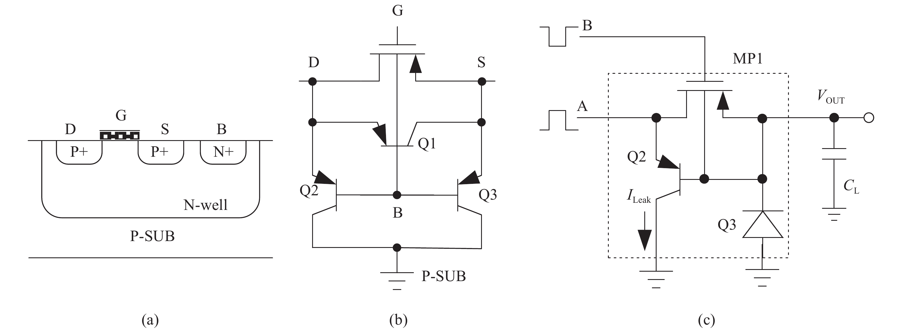
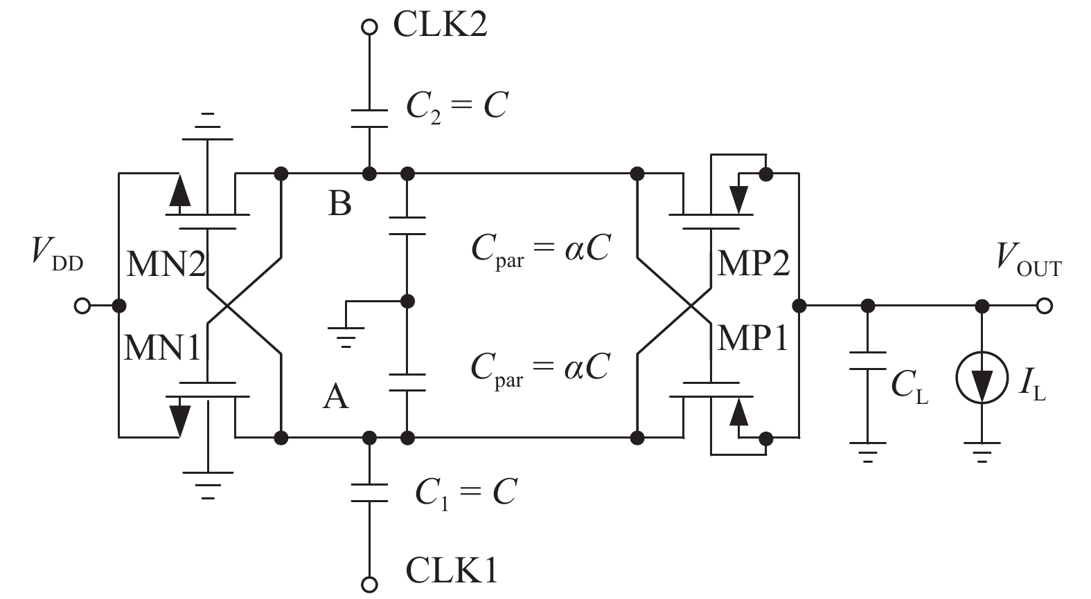
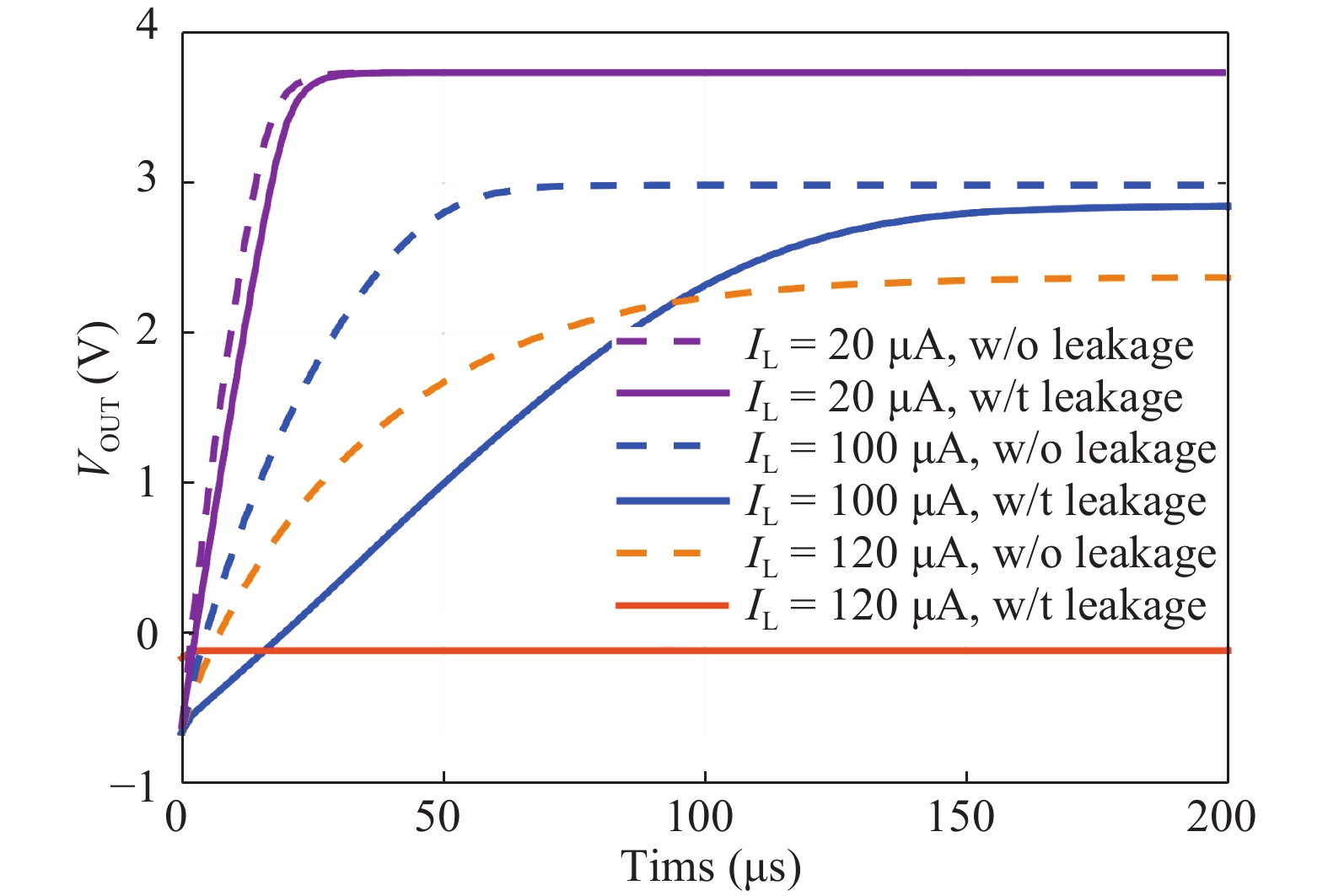


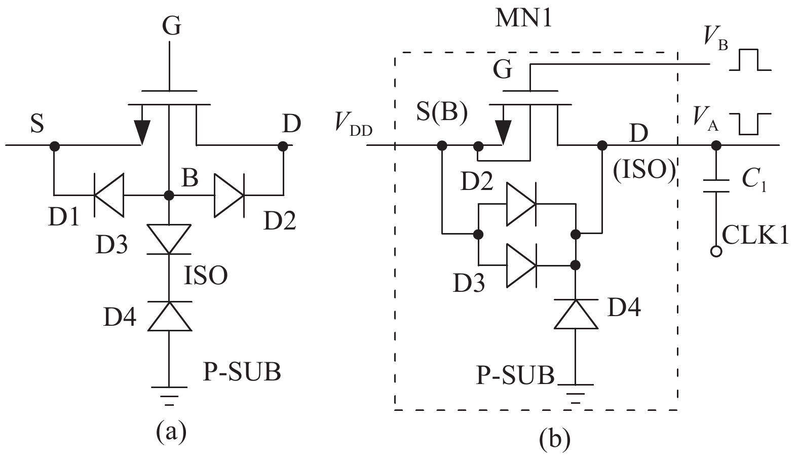

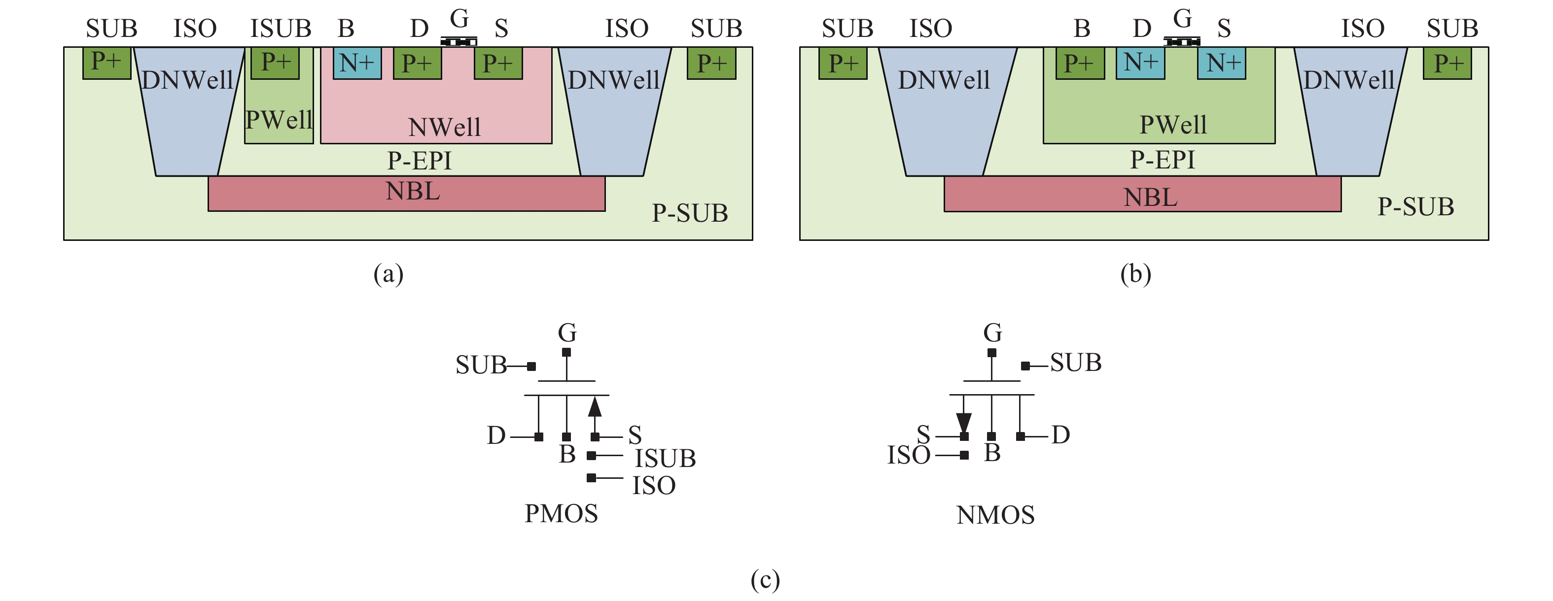
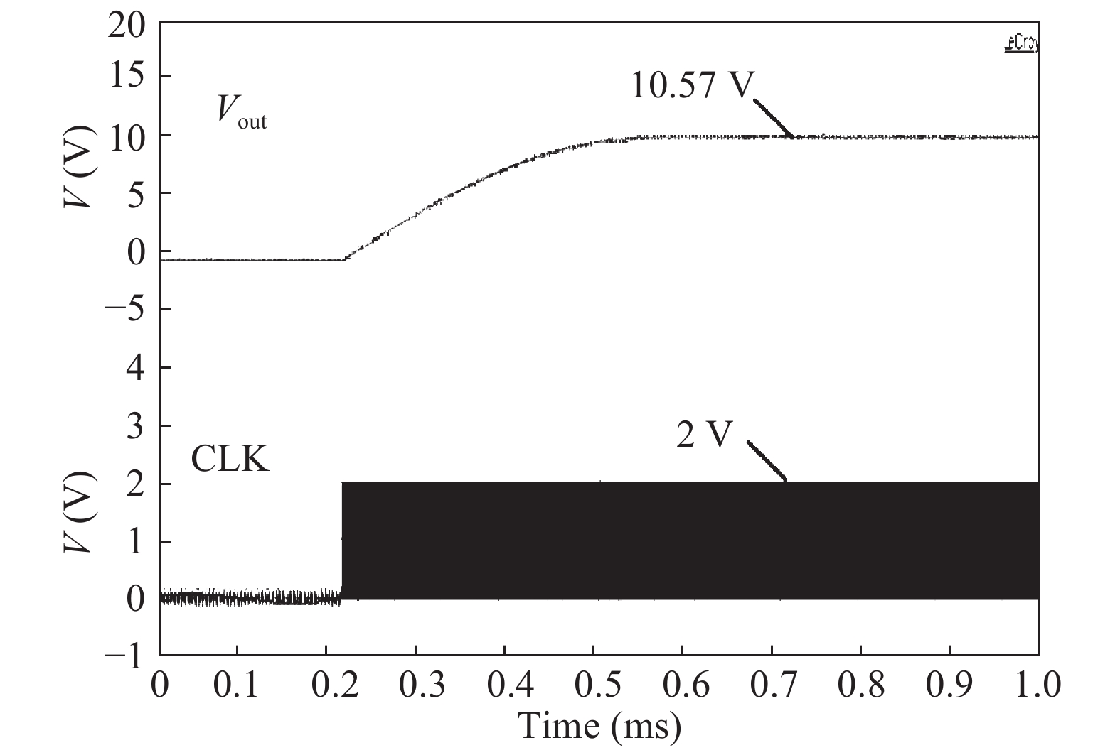
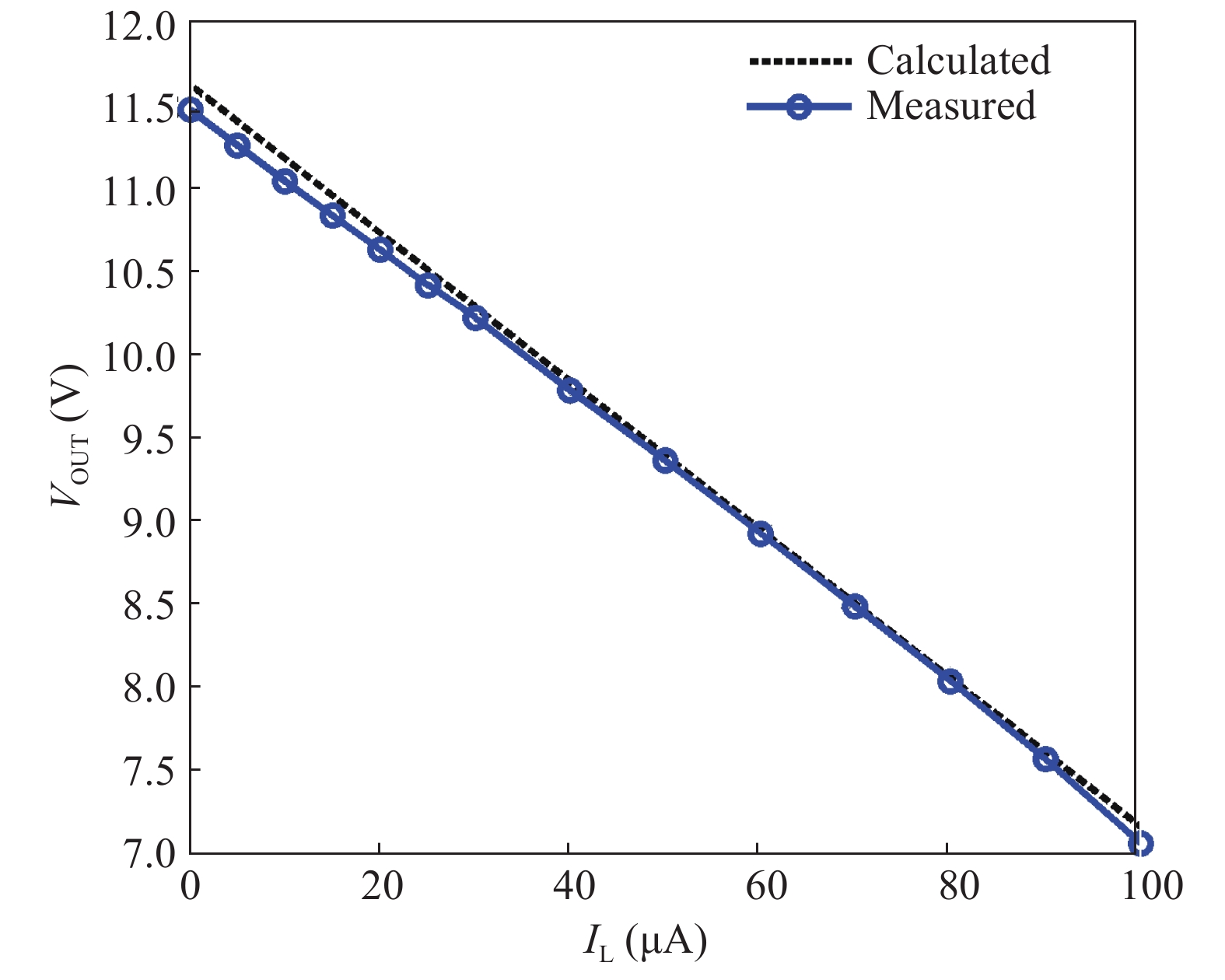

Table 1. Performance summary and comparison.
| Parameter | Ref. [17] | Ref. [18] | Ref. [19] | Ref. [20] | Ref. [21] | This work |
| Technology (μm) | 0.18-CMOS
(with deep N-well) |
0.8 HV-CMOS | 0.7 CMOS | 0.35 BCD | 0.13-CMOS
(with deep N-well) |
0.35 BCD |
| Area (mm2) | – | 4.4* | 0.15 | – | 0.066 | 0.56 |
| Clock freq. (MHz) | 100 | 0.033 | 10 | 10 | 0.25 | 1 |
| Flying capacitance | On-chip 2.5 pF | Off-chip
0.47 μF |
On-chip
100 pF (MOS) |
On-chip 10 pF (MOS) | Off-chip 10 nF | On-chip 56 pF (MIM) |
| Supply voltage (V) | 1.8 | 2.5 | 3 | 3.7 | 0.18 | 2 |
| Number of stages | 5 | 3 | 1 | 36 | 3 | 5 |
| Output voltage (V) | 10.1 (@IL = 0 ) | 9.06
(@IL = 100 μA) |
5.9
(@IL = 0) |
105
(@IL = 100 μA) |
0.619
(@IL = 0) |
11.5
(@IL = 0) |
| Max. power eff. (%) | 50 | 90.6 | 75 | 39** | 34 | 72.6 |
| IOUT @ Max. eff. (μA) | 350 | 100 | – | 100 | 21 | 40 |
| * Overall area including 2 charge pumps and other system level blocks. ** Simulation results. | ||||||
 DownLoad: CSV
| [1] |
Nagaraj S, Rassam F G. Improved noncoherent UWB receiver for implantable biomedical devices. IEEE Trans Biomed Eng, 2016, 63(10): 2220 doi: 10.1109/TBME.2015.2511538
|
| [2] |
Zhou J, Kim A, Ziaie B. An ultrasonically controlled power management system for implantable biomedical devices. IEEE Biomed Circuits Syst Conf, 2015: 1
|
| [3] |
Lee S Y, Hong J H, Hsieh C H, et al. A Low-power 13.56 MHz RF front-end circuit for implantable biomedical devices. IEEE Trans Biomed Circuits Syst, 2013, 7(3): 256 doi: 10.1109/TBCAS.2012.2212276
|
| [4] |
Wong L S Y, Hossain S, Ta A, et al. A very low-power CMOS mixed-signal IC for implantable pacemaker applications. IEEE J Solid-State Circuits, 2004, 39(12): 2446 doi: 10.1109/JSSC.2004.837027
|
| [5] |
Zhang J, Zhang H, Zhang R, et al. A mixed-signal ASIC for triple-chamber cardiac pacemakers with heart resistance measurement. IEEE Asian Solid-State Circuits Conference, 2015: 1
|
| [6] |
Yip M, Jin R, Nakajima H H, et al. A fully-implantable cochlear implant SoC with piezoelectric middle-ear sensor and arbitrary waveform neural stimulation. IEEE J Solid-State Circuits, 2015, 50(1): 214 doi: 10.1109/JSSC.2014.2355822
|
| [7] |
Azin M, Guggenmos D J, Barbay S, et al. A battery-powered activity-dependent intracortical microstimulation IC for brain-machine-brain Interface. IEEE J Solid-State Circuits, 2011, 46(4): 731 doi: 10.1109/JSSC.2011.2108770
|
| [8] |
Novo A, Gerosa A, Neviani A, et al. Programmable voltage multiplier for pacemaker output pulse generation. Electron Lett, 1999, 35(7): 560 doi: 10.1049/el:19990369
|
| [9] |
Novo A, Gerosa A, Neviani A, et al. A CMOS 0.8 μm programmable charge pump for the output stage of an implantable pacemaker. IEEE International Caracas Conference on Devices, Circuits and Systems, 2000: 34/1
|
| [10] |
Gak J, Miguez M, Arnaud A. A programmable charge pump voltage converter for implantable medical devices in a HV technology. IEEE Latin American Symposium on Circuits and Systems, 2013: 1
|
| [11] |
Esmailiyan A, Shaker A, Ghotbi I, et al. A charge-pump based multi-mode stimuli generator for cardiac pacemaking. IEEE International New Circuits and Systems Conference, 2016: 1
|
| [12] |
Tanzawa T, Tanaka T. A dynamic analysis of the Dickson charge pump circuit. IEEE J Solid-State Circuits, 1997, 32(8): 1231 doi: 10.1109/4.604079
|
| [13] |
Baek J M, Chun J H, Kwon K W. A power-efficient voltage upconverter for embedded EEPROM application. IEEE Trans Circuits Syst II, 2010, 57(6): 435 doi: 10.1109/TCSII.2010.2048351
|
| [14] |
Peng H, Tang N, Yang Y, et al. CMOS startup charge pump with body bias and backward control for energy harvesting step-up converters. IEEE Trans Circuits Syst I, 2014, 61(6): 1618 doi: 10.1109/TCSI.2013.2290823
|
| [15] |
Tanzawa T. An optimum design for integrated switched-capacitor Dickson charge pump multipliers with area power balance. IEEE Trans Power Electron, 2014, 29(2): 534 doi: 10.1109/TPEL.2013.2271279
|
| [16] |
Nakagome Y, Tanaka H, Takeuchi K, et al. An experimental 1.5-V 64-Mb DRAM. IEEE J Solid-State Circuits, 1991, 26(4): 465 doi: 10.1109/4.75040
|
| [17] |
Pelliconi R, Iezzi D, Baroni A, et al. Power efficient charge pump in deep submicron standard CMOS technology. IEEE J Solid-State Circuits, 2003, 38(6): 1068 doi: 10.1109/JSSC.2003.811991
|
| [18] |
Ying T, Ki W, Chan M. Area-efficient CMOS charge pumps for LCD drivers. IEEE J Solid-State Circuits, 2003, 8(10): 1721
|
| [19] |
Favrat P, Deval P, Declercq M J. A high-efficiency CMOS voltage doubler. IEEE J Solid-State Circuits, 1998, 33(3): 410
|
| [20] |
Shen L, Hofmann K. Fully integratable 4-phase charge pump architecture for high voltage applications. International Conference Mixed Design of Integrated Circuits and Systems, 2012: 265
|
| [21] |
Kim J, Mok P K T, Kim C. A 0.15 V input energy harvesting charge pump with dynamic body biasing and adaptive dead-time for efficiency improvement. IEEE J Solid-State Circuits, 2015, 50(2): 414 doi: 10.1109/JSSC.2014.2375824
|


Article views: 8564 Times PDF downloads: 552 Times Cited by: 0 Times
Received: 02 March 2018 Revised: 03 April 2018 Online: Uncorrected proof: 28 May 2018Published: 09 October 2018
| Citation: |
Jie Zhang, Hong Zhang, Ruizhi Zhang. A high-efficiency charge pump in BCD process for implantable medical devices[J]. Journal of Semiconductors, 2018, 39(10): 105003. doi: 10.1088/1674-4926/39/10/105003
****
J Zhang, H Zhang, R Z Zhang, A high-efficiency charge pump in BCD process for implantable medical devices[J]. J. Semicond., 2018, 39(10): 105003. doi: 10.1088/1674-4926/39/10/105003.

|
| [1] |
Nagaraj S, Rassam F G. Improved noncoherent UWB receiver for implantable biomedical devices. IEEE Trans Biomed Eng, 2016, 63(10): 2220 doi: 10.1109/TBME.2015.2511538
|
| [2] |
Zhou J, Kim A, Ziaie B. An ultrasonically controlled power management system for implantable biomedical devices. IEEE Biomed Circuits Syst Conf, 2015: 1
|
| [3] |
Lee S Y, Hong J H, Hsieh C H, et al. A Low-power 13.56 MHz RF front-end circuit for implantable biomedical devices. IEEE Trans Biomed Circuits Syst, 2013, 7(3): 256 doi: 10.1109/TBCAS.2012.2212276
|
| [4] |
Wong L S Y, Hossain S, Ta A, et al. A very low-power CMOS mixed-signal IC for implantable pacemaker applications. IEEE J Solid-State Circuits, 2004, 39(12): 2446 doi: 10.1109/JSSC.2004.837027
|
| [5] |
Zhang J, Zhang H, Zhang R, et al. A mixed-signal ASIC for triple-chamber cardiac pacemakers with heart resistance measurement. IEEE Asian Solid-State Circuits Conference, 2015: 1
|
| [6] |
Yip M, Jin R, Nakajima H H, et al. A fully-implantable cochlear implant SoC with piezoelectric middle-ear sensor and arbitrary waveform neural stimulation. IEEE J Solid-State Circuits, 2015, 50(1): 214 doi: 10.1109/JSSC.2014.2355822
|
| [7] |
Azin M, Guggenmos D J, Barbay S, et al. A battery-powered activity-dependent intracortical microstimulation IC for brain-machine-brain Interface. IEEE J Solid-State Circuits, 2011, 46(4): 731 doi: 10.1109/JSSC.2011.2108770
|
| [8] |
Novo A, Gerosa A, Neviani A, et al. Programmable voltage multiplier for pacemaker output pulse generation. Electron Lett, 1999, 35(7): 560 doi: 10.1049/el:19990369
|
| [9] |
Novo A, Gerosa A, Neviani A, et al. A CMOS 0.8 μm programmable charge pump for the output stage of an implantable pacemaker. IEEE International Caracas Conference on Devices, Circuits and Systems, 2000: 34/1
|
| [10] |
Gak J, Miguez M, Arnaud A. A programmable charge pump voltage converter for implantable medical devices in a HV technology. IEEE Latin American Symposium on Circuits and Systems, 2013: 1
|
| [11] |
Esmailiyan A, Shaker A, Ghotbi I, et al. A charge-pump based multi-mode stimuli generator for cardiac pacemaking. IEEE International New Circuits and Systems Conference, 2016: 1
|
| [12] |
Tanzawa T, Tanaka T. A dynamic analysis of the Dickson charge pump circuit. IEEE J Solid-State Circuits, 1997, 32(8): 1231 doi: 10.1109/4.604079
|
| [13] |
Baek J M, Chun J H, Kwon K W. A power-efficient voltage upconverter for embedded EEPROM application. IEEE Trans Circuits Syst II, 2010, 57(6): 435 doi: 10.1109/TCSII.2010.2048351
|
| [14] |
Peng H, Tang N, Yang Y, et al. CMOS startup charge pump with body bias and backward control for energy harvesting step-up converters. IEEE Trans Circuits Syst I, 2014, 61(6): 1618 doi: 10.1109/TCSI.2013.2290823
|
| [15] |
Tanzawa T. An optimum design for integrated switched-capacitor Dickson charge pump multipliers with area power balance. IEEE Trans Power Electron, 2014, 29(2): 534 doi: 10.1109/TPEL.2013.2271279
|
| [16] |
Nakagome Y, Tanaka H, Takeuchi K, et al. An experimental 1.5-V 64-Mb DRAM. IEEE J Solid-State Circuits, 1991, 26(4): 465 doi: 10.1109/4.75040
|
| [17] |
Pelliconi R, Iezzi D, Baroni A, et al. Power efficient charge pump in deep submicron standard CMOS technology. IEEE J Solid-State Circuits, 2003, 38(6): 1068 doi: 10.1109/JSSC.2003.811991
|
| [18] |
Ying T, Ki W, Chan M. Area-efficient CMOS charge pumps for LCD drivers. IEEE J Solid-State Circuits, 2003, 8(10): 1721
|
| [19] |
Favrat P, Deval P, Declercq M J. A high-efficiency CMOS voltage doubler. IEEE J Solid-State Circuits, 1998, 33(3): 410
|
| [20] |
Shen L, Hofmann K. Fully integratable 4-phase charge pump architecture for high voltage applications. International Conference Mixed Design of Integrated Circuits and Systems, 2012: 265
|
| [21] |
Kim J, Mok P K T, Kim C. A 0.15 V input energy harvesting charge pump with dynamic body biasing and adaptive dead-time for efficiency improvement. IEEE J Solid-State Circuits, 2015, 50(2): 414 doi: 10.1109/JSSC.2014.2375824
|

 WeChat ID
Journal of Semiconductors © 2017 All Rights Reserved 京ICP备05085259号-2