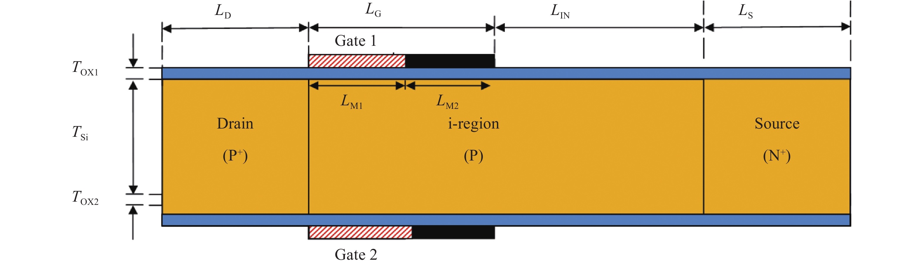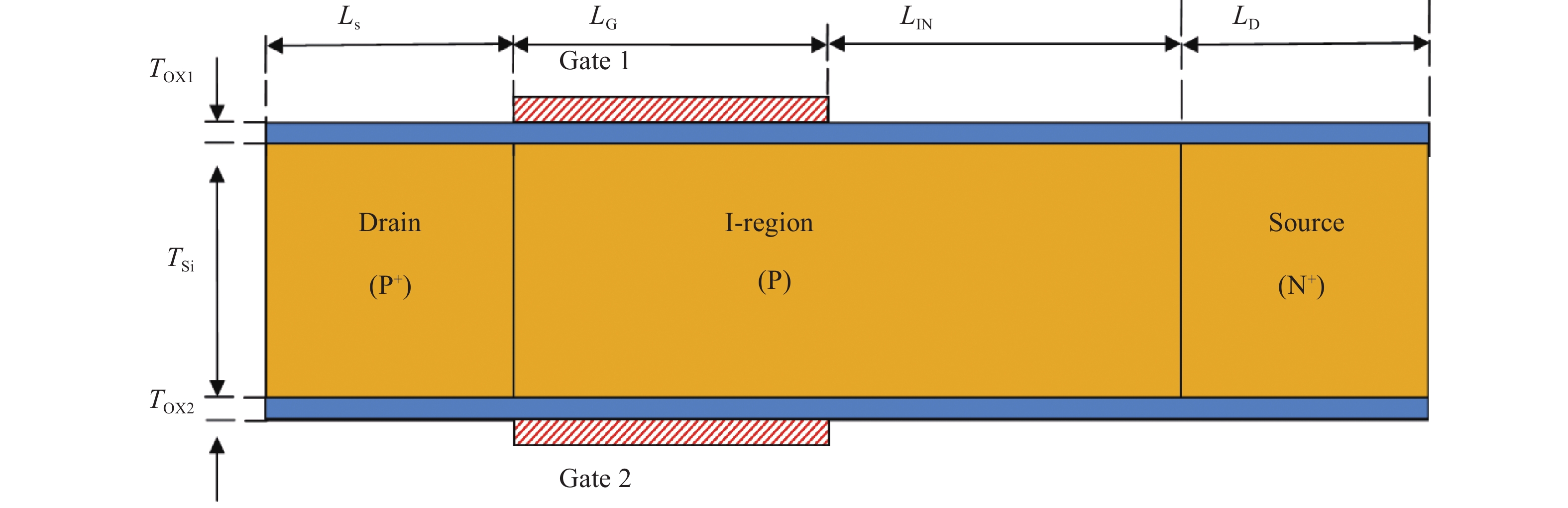
Fig. 1.
(Color online) The structure of the simulated DG-PIMOS[8].
SEMICONDUCTOR DEVICES
Sarabdeep Singh, Ashish Raman and Naveen Kumar
Corresponding author: Ashish Raman, E-mail: ramana@nitj.ac.in
Abstract: An impact ionization MOSFET (IMOS) is evolved for overcoming the constraint of less than 60 mV/decade sub-threshold slope (SS) of conventional MOSFET at room temperature. In this work, first, the device performance of the p-type double gate impact ionization MOSFET (DG-IMOS) is optimized by adjusting the device design parameters. The adjusted parameters are ratio of gate and intrinsic length, gate dielectric thickness and gate work function. Secondly, the DMG (dual material gate) DG-IMOS is proposed and investigated. This DMG DG-IMOS is further optimized to obtain the best possible performance parameters. Simulation results reveal that DMG DG-IMOS when compared to DG-IMOS, shows better ION, ION/IOFF ratio, and RF parameters. Results show that by properly tuning the lengths of two materials at a ratio of 1.5 in DMG DG-IMOS, optimized performance is achieved including ION/IOFF ratio of 2.87 × 10⁹ A/μm with ION as 11.87 × 10⁻⁴ A/μm and transconductance of 1.06×10⁻³ S/μm. It is analyzed that length of drain side material should be greater than the length of source side material to attain the higher transconductance in DMG DG-IMOS.
Key words: impact ionization MOSFET (IMOS), avalanche breakdown, sub-threshold slope, dual material gate (DMG), biosensor
| [1] |
Gopalakrishnan K, Griffin P B, Plummer J D. I-MOS: a novel semiconductor device with a subthreshold slope lower than kT/q. IEEE Electron Devices Meeting, 2002: 289
|
| [2] |
Gopalakrishnan K, Griffin P B, Plummer J D. Impact ionization MOS (I-MOS)-Part I: device and circuit simulations. IEEE Trans Eelectron devices, 2005, 52(1): 69 doi: 10.1109/TED.2004.841344
|
| [3] |
Saad I, Zuhir H M, Seng C B, et al. Characterization of vertical strained SiGe impact ionization MOSFET for ultra-sensitive biosensor application. IEEE International Conference on Semiconductor Electronics, 2014: 154
|
| [4] |
Singh S, Kondekar P N. Analytical modeling of Schottky tunneling source impact ionization MOSFET with reduced breakdown voltage. Eng Sci Technol, 2016, 19(1): 421
|
| [5] |
Choi W Y, Song J Y, Lee J D, et al. A novel biasing scheme for I-MOS (impact-ionization MOS) devices. IEEE Trans Nanotechnol, 2005, 4(3): 322 doi: 10.1109/TNANO.2005.847001
|
| [6] |
Ramaswamy S, Kumar M J. Junctionless impact ionization MOS: proposal and investigation. IEEE Trans Electron Devices, 2014, 61(12): 4295 doi: 10.1109/TED.2014.2361343
|
| [7] |
Hassani FA, Fathipour M, Mehran M. A comparison study between double and single gate p-IMOS. IEEE AFRICON 2007 :1.
|
| [8] |
ATLAS Device Simulation Software, Silvaco International, Santa Clara, CA, USA, 2014
|
| [9] |
Dixit A, Singh S, Kondekar P N, et al. Parameters optimization of lateral impact ionization MOS (LIMOS). IEEE Global High Tech Congress on Electronics (GHTCE), 2013: 56
|
| [10] |
Long W, Ou H, Kuo J M, et al. Dual-material gate (DMG) field effect transistor. IEEE Trans Electron Devices, 1999, 46(5): 865 doi: 10.1109/16.760391
|
| [11] |
Zhou X, Long W. A novel hetero-material gate (HMG) MOSFET for deep-submicron ULSI technology. IEEE Transactions on Electron Devices. 1998, 45(12): 2546 doi: 10.1109/16.735743
|
| [12] |
Amin SI, Sarin RK. Charge-plasma based dual-material and gate-stacked architecture of junctionless transistor for enhanced analog performance. Superlattices Microstruct, 2015, 88: 582 doi: 10.1016/j.spmi.2015.10.017
|
| [13] |
Sharma S K, Raj B, Khosla M. Subthreshold performance of In1-xGax as based dual metal with gate stack cylindrical/surrounding gate nanowire MOSFET for low power analog applications. J Nanoelectron Optoelectron, 2017, 12(2): 171 doi: 10.1166/jno.2017.1961
|
| [14] |
Kumar S, Raj B. Analysis of ION and ambipolar current for dual-material gate-drain overlapped DG-TFET. J Nanoelectron Optoelectron, 2016, 11(3): 323 doi: 10.1166/jno.2016.1902
|
| [15] |
Anand S, Sarin RK. Dual material gate doping-less tunnel FET with hetero gate dielectric for enhancement of analog/RF performance. J Semicond, 2017, 38(2): 024001 doi: 10.1088/1674-4926/38/2/024001
|
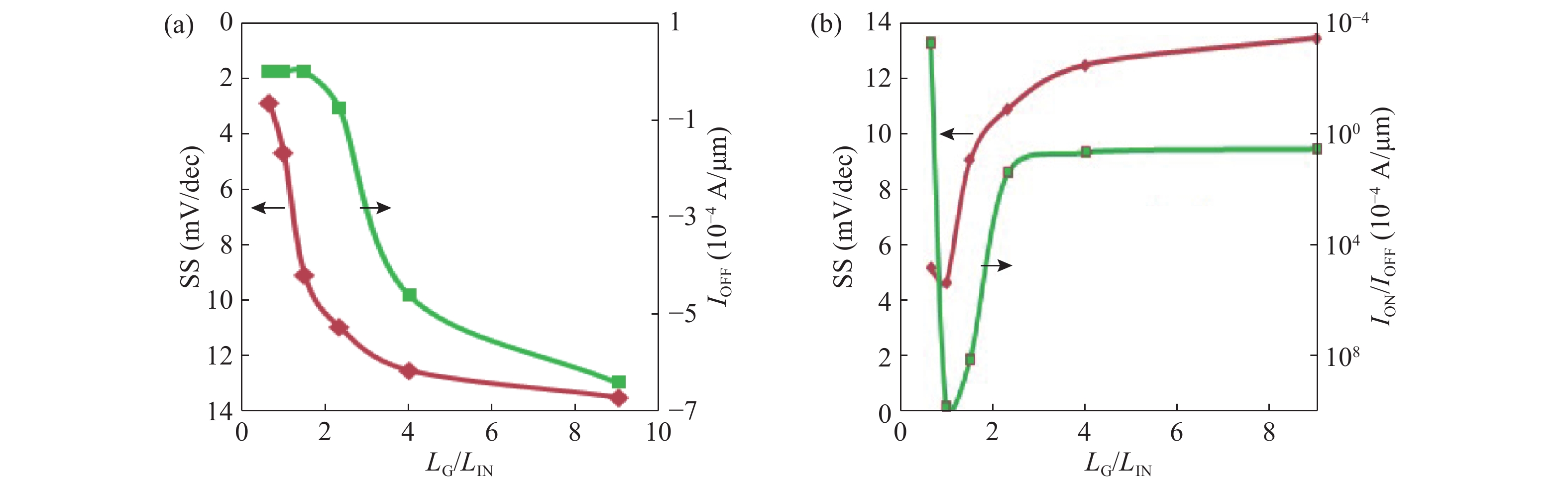
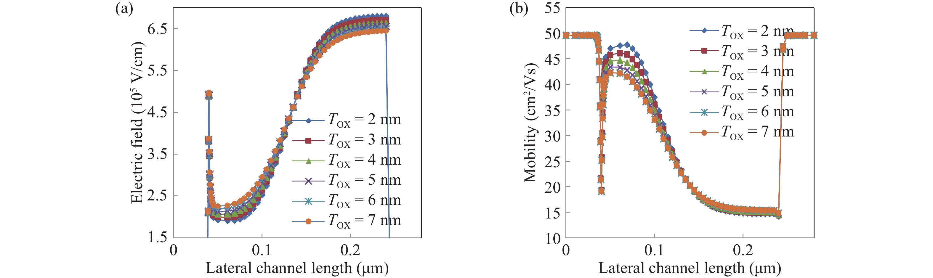
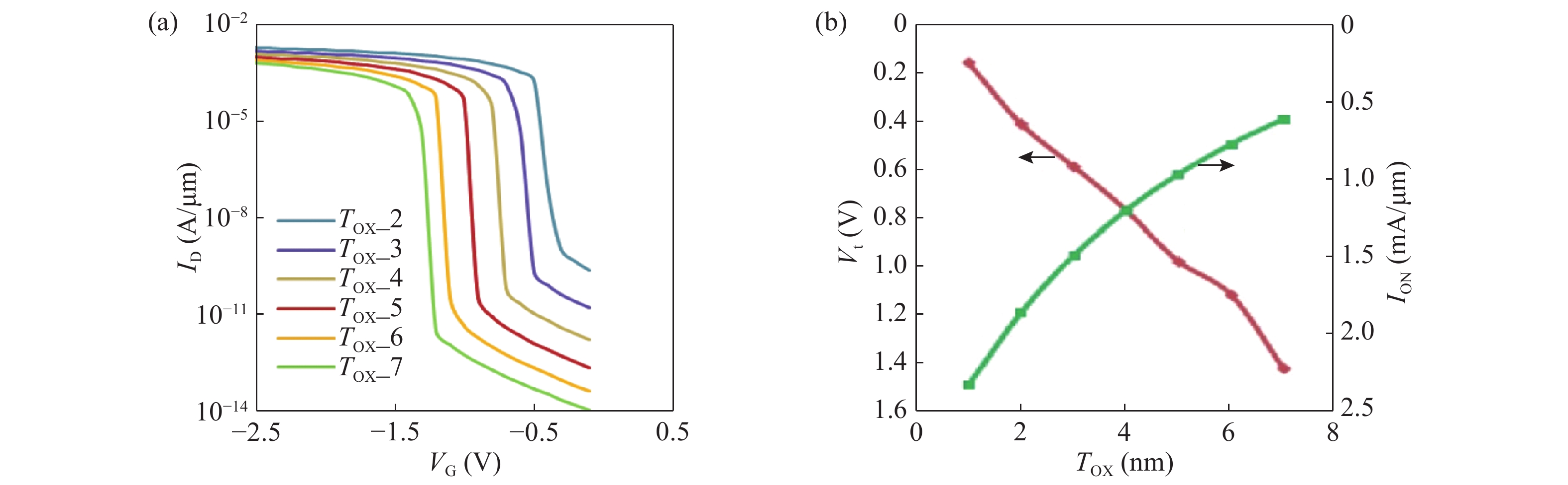
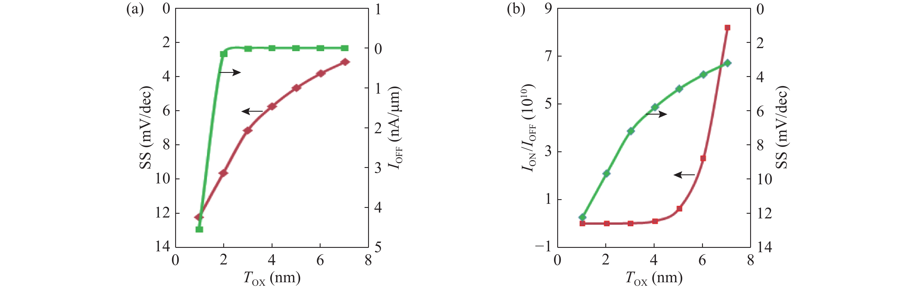
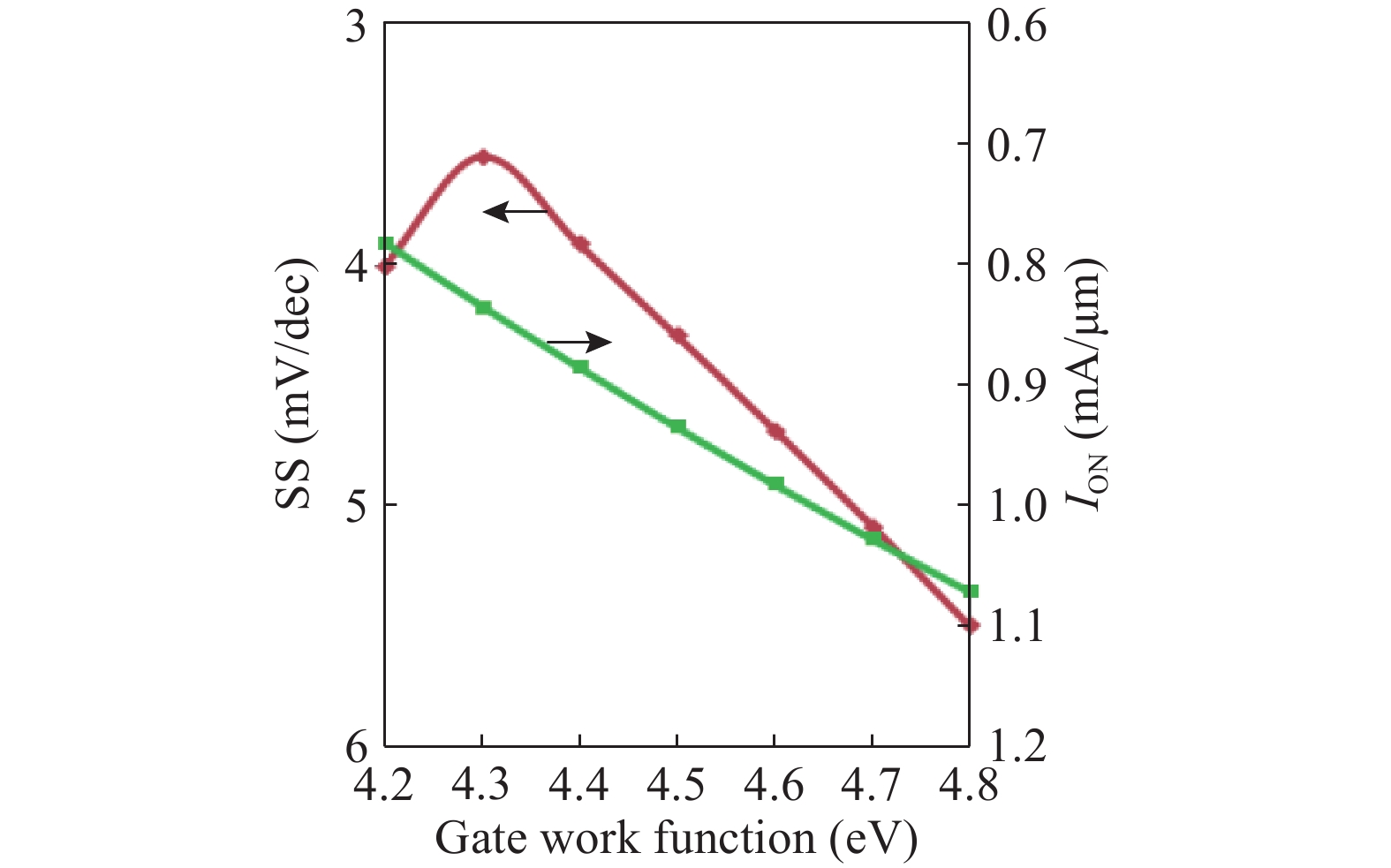
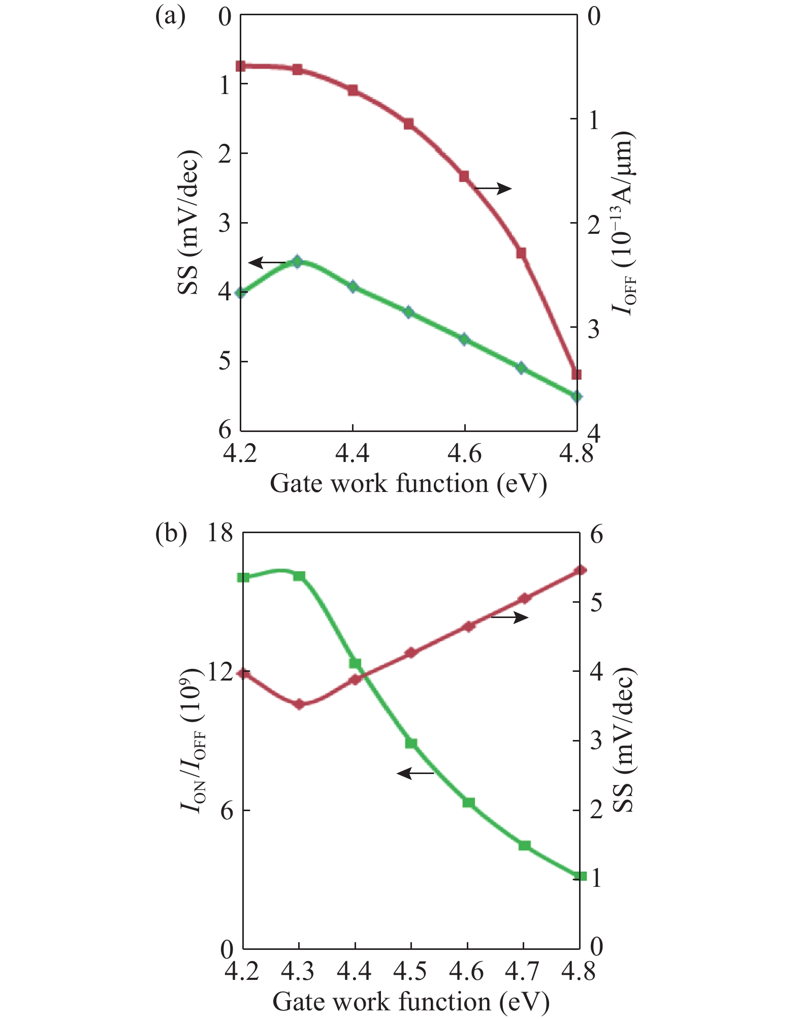
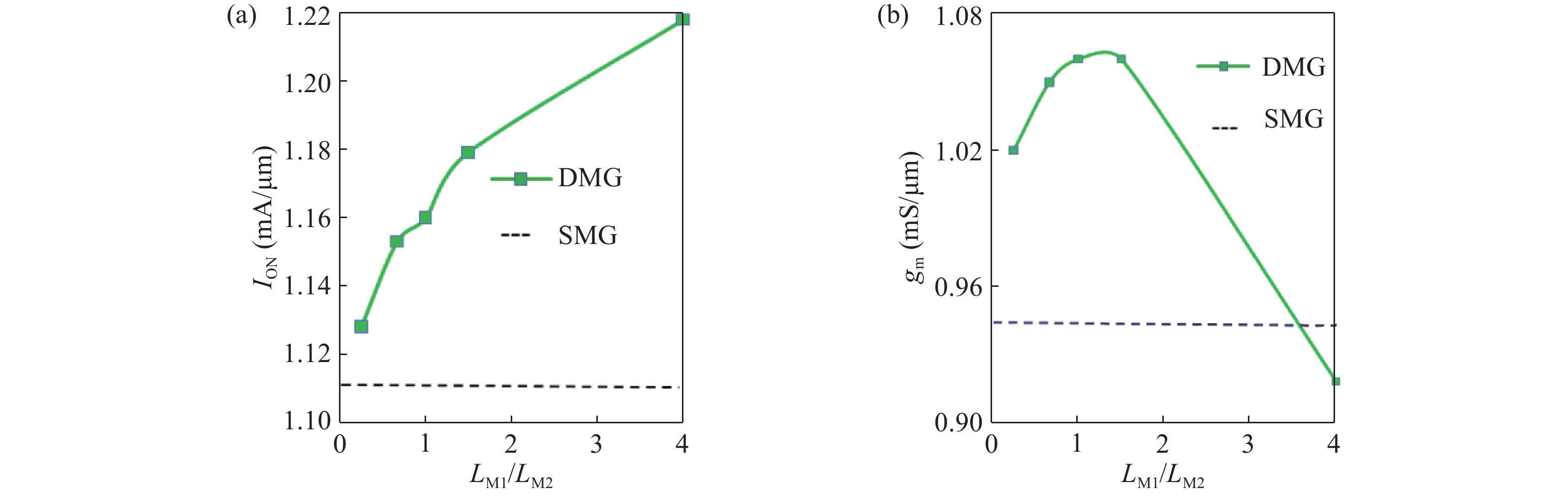
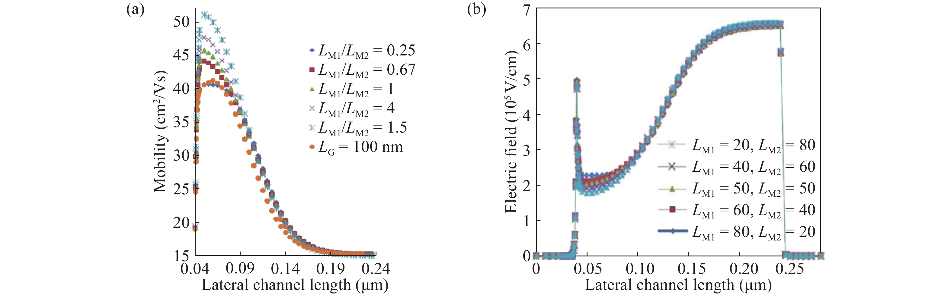
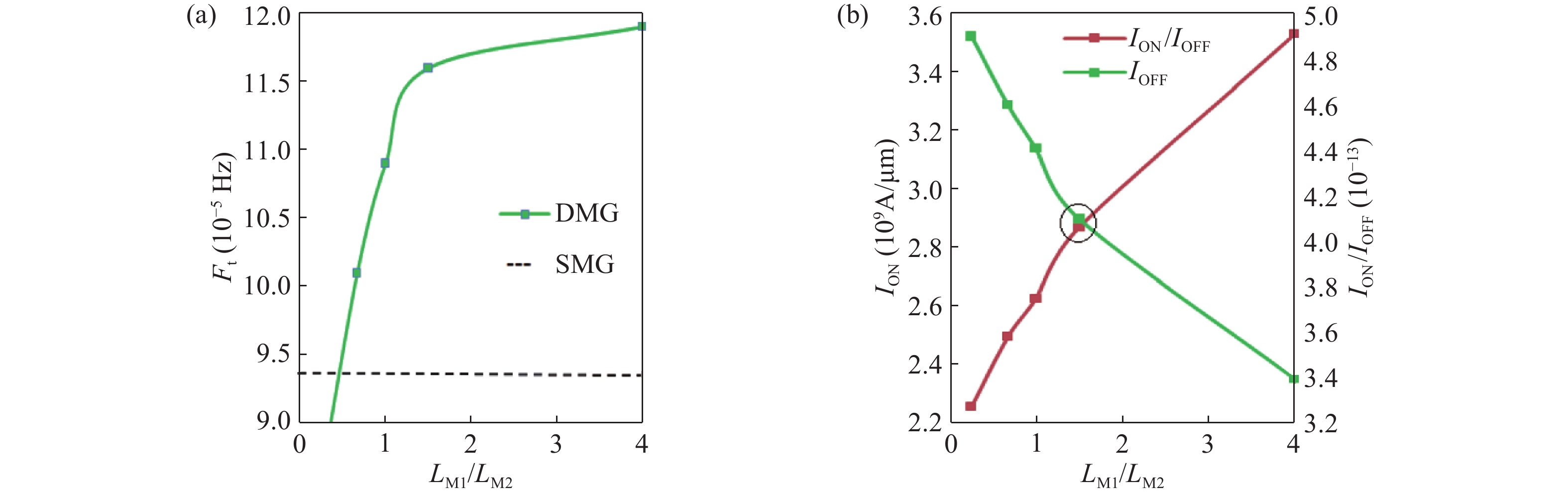
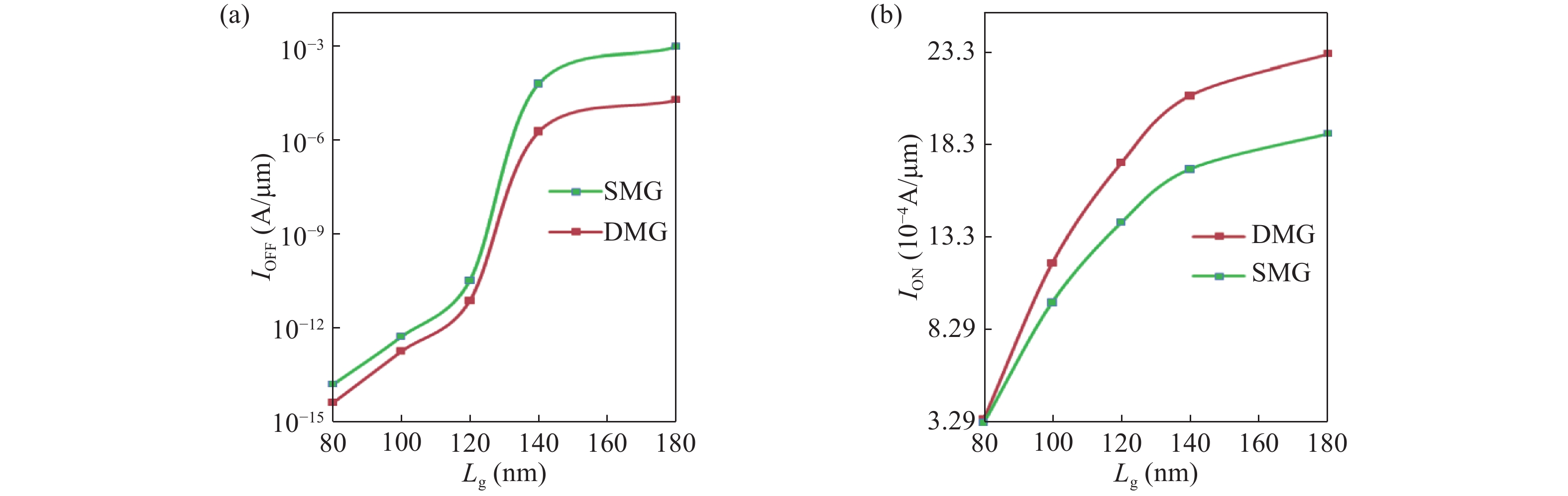
Table 1. Parameters used for DG-IMOS Simulations.
| Parameter | DG-IMOS |
| Gate length, LG (nm) | 100 |
| Intrinsic length, LIN (nm) | 100 |
| Gate oxide thickness, TOX (nm) | 5 |
| Source doping NA (cm−3) | 1 × 10²⁰ |
| Drain doping ND (cm−3) | 1 × 10²⁰ |
| Gate work function (eV) | 4.6 |
| Gate bias (V) | 0–2.5 |
 DownLoad: CSV
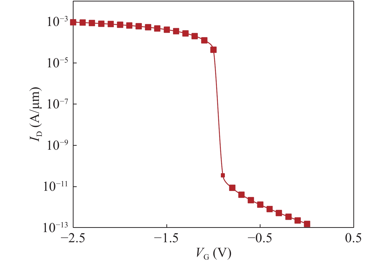
Table 2. Parameters at various ratios of LG/LIN.
| Parameter | LG/LIN = 0.66 | LG/LIN = 1 | LG/LIN = 1.5 | LG/LIN = 2.33 | LG/LIN = 4 | LG/LIN = 9 |
| SS (mV/dec) | 5.2 | 4.68 | 9.09 | 10.96 | 12.53 | 13.51 |
| ION (A/μm) | 4.18 × 10⁻¹¹ | 9.81 × 10⁻⁴ | 1.45 × 10⁻³ | 1.76 × 10⁻³ | 1.96 × 10⁻³ | 2.00 × 10⁻³ |
| IOFF (A/μm) | 8.89 × 10⁻¹⁶ | 1.55 × 10⁻¹³ | 1.13 × 10⁻¹¹ | 7.57 × 10⁻⁵ | 4.60 × 10⁻⁴ | 6.40 × 10⁻⁴ |
| ION/IOFF | 4.7 × 10⁴ | 6.34 × 10⁹ | 1.29 × 10⁸ | 23.17 | 4.25 | 3.11 |
DownLoad: CSV
Table 3. Parameters at variations in TOX.
| Parameter | TOX = 2 nm | TOX = 3 nm | TOX = 4 nm | TOX = 5 nm | TOX = 6 nm | TOX = 7 nm |
| SS (mV/dec) | 9.67 | 7.17 | 5.77 | 4.68 | 3.84 | 3.17 |
| Vt (V) | −0.42 | −0.596 | −0.77 | −0.98 | −0.11 | −1.43 |
| ION (A/μm) | 1.87 × 10⁻³ | 1.50 × 10⁻³ | 1.21 × 10⁻³ | 9.81 × 10⁻⁴ | 7.88 × 10⁻⁴ | 6.28 × 10⁻⁴ |
| IOFF (A/μm) | 1.52 × 10⁻¹⁰ | 1.09 × 10⁻¹¹ | 1.12 × 10⁻¹² | 1.55 × 10⁻¹³ | 2.86 × 10⁻¹⁴ | 7.62 × 10⁻¹⁵ |
| ION/IOFF | 1.23 × 10⁷ | 1.38 × 10⁸ | 1.09 × 10⁹ | 6.34 × 10⁹ | 2.76 × 10¹⁰ | 8.25 × 10¹⁰ |
DownLoad: CSV
Table 4. Parameters of different work functions of gate.
| Work function | 4.2 | 4.3 | 4.4 | 4.5 | 4.6 | 4.7 | 4.8 |
| SS (mV/dec) | 4 | 3.55 | 3.91 | 4.29 | 4.68 | 5.08 | 5.49 |
| Vt (V) | −1.35 | −1.25 | −1.14 | −1.05 | −0.98 | −0.85 | −0.72 |
| ION (A/μm) | 7.82 × 10⁻⁴ | 8.35 × 10⁻⁴ | 8.85 × 10⁴ | 9.34 × 10⁻⁴ | 9.81 × 10⁻⁴ | 1.03 × 10⁻³ | 1.07 × 10⁻³ |
| IOFF (A/μm) | 4.83 × 10⁻¹⁴ | 5.15 × 10⁻¹⁴ | 7.13 × 10⁻¹⁴ | 1.04 × 10⁻¹³ | 1.55 × 10⁻¹³ | 2.29 × 10⁻¹³ | 3.45 × 10⁻¹³ |
| ION/IOFF | 1.62 × 10¹⁰ | 1.62 × 10¹⁰ | 1.24 × 10¹⁰ | 8.94 × 10⁹ | 6.34 × 10⁹ | 4.48 × 10⁹ | 3.10 × 10⁹ |
DownLoad: CSV
Table 5. Parameters of different LM1/LM2 ratios.
| LM1/LM2 | 0.25 | 0.67 | 1 | 1.5 | 4 |
| SS (mV/dec) | 4.94 | 5.14 | 5.14 | 5.25 | 5.58 |
| Vt (V) | −1.07 | −1.07 | −1.07 | −0.95 | −0.82 |
| ION (A/μm) | 1.13 × 10⁻³ | 1.15 × 10⁻³ | 1.16 × 10⁻³ | 1.18 × 10⁻³ | 1.22 × 10⁻³ |
| IOFF (A/μm) | 4.90 × 10⁻¹³ | 4.60 × 10⁻¹³ | 4.41 × 10⁻¹³ | 4.10 × 10⁻¹³ | 3.40 × 10⁻¹³ |
| ION/IOFF | 2.26 × 10⁹ | 2.50 × 10⁹ | 2.63 × 10⁹ | 2.87 × 10⁹ | 3.53 × 10⁹ |
| gm (S/μm) | 1.02 × 10⁻³ | 1.05 × 10⁻³ | 1.06 × 10⁻³ | 1.06 × 10⁻³ | 9.18 × 10⁻³ |
| ft (Hz) | 8.62 × 10⁻⁵ | 1.01 × 10⁻⁴ | 1.09 × 10⁻⁴ | 1.16 × 10⁻⁴ | 1.19 × 10⁻⁴ |
DownLoad: CSV
Table 6. Comparision table of parameters forvarying LG.
| LG (nm) | ION (A/μm) | IOFF (A/μm) | ION/IOFF | gm (S/μm) | |||||||
| SMG | DMG | SMG | DMG | SMG | DMG | SMG | DMG | ||||
| 80 | 3.29 × 10⁻⁴ | 3.50 × 10⁻⁴ | 1.55 × 10⁻¹⁴ | 5.14 × 10⁻¹⁵ | 2.12 × 10¹⁰ | 6.87 × 10¹⁰ | 5.58 × 10⁻⁴ | 5.99 × 10⁻⁴ | |||
| 100 | 1.12 × 10⁻³ | 1.18 × 10⁻³ | 5.20 × 10⁻¹³ | 4.10 × 10⁻¹³ | 2.14 × 10⁹ | 2.87 × 10⁹ | 9.41 × 10⁻⁴ | 1.06 × 10⁻³ | |||
| 120 | 1.64 × 10⁻³ | 1.71 × 10⁻³ | 3.07 × 10⁻¹¹ | 2.97 × 10⁻¹¹ | 5.32 × 10⁷ | 5.76 × 10⁷ | 1.13 × 10⁻³ | 9.53 × 10⁻⁴ | |||
| 140 | 1.99 × 10⁻³ | 2.07 × 10⁻³ | 5.20 × 10⁻⁵ | 5.03 × 10⁻⁵ | 3.75 × 101 | 4.10 × 101 | 1.30 × 10⁻³ | 1.28 × 10⁻³ | |||
| 180 | 2.22 × 10⁻³ | 2.29 × 10⁻³ | 7.70 × 10⁻⁴ | 7.20 × 10⁻⁴ | 2.80 | 3.17 | 8.22 × 10⁻⁴ | 8.20 × 10⁻⁴ | |||
DownLoad: CSV
| [1] |
Gopalakrishnan K, Griffin P B, Plummer J D. I-MOS: a novel semiconductor device with a subthreshold slope lower than kT/q. IEEE Electron Devices Meeting, 2002: 289
|
| [2] |
Gopalakrishnan K, Griffin P B, Plummer J D. Impact ionization MOS (I-MOS)-Part I: device and circuit simulations. IEEE Trans Eelectron devices, 2005, 52(1): 69 doi: 10.1109/TED.2004.841344
|
| [3] |
Saad I, Zuhir H M, Seng C B, et al. Characterization of vertical strained SiGe impact ionization MOSFET for ultra-sensitive biosensor application. IEEE International Conference on Semiconductor Electronics, 2014: 154
|
| [4] |
Singh S, Kondekar P N. Analytical modeling of Schottky tunneling source impact ionization MOSFET with reduced breakdown voltage. Eng Sci Technol, 2016, 19(1): 421
|
| [5] |
Choi W Y, Song J Y, Lee J D, et al. A novel biasing scheme for I-MOS (impact-ionization MOS) devices. IEEE Trans Nanotechnol, 2005, 4(3): 322 doi: 10.1109/TNANO.2005.847001
|
| [6] |
Ramaswamy S, Kumar M J. Junctionless impact ionization MOS: proposal and investigation. IEEE Trans Electron Devices, 2014, 61(12): 4295 doi: 10.1109/TED.2014.2361343
|
| [7] |
Hassani FA, Fathipour M, Mehran M. A comparison study between double and single gate p-IMOS. IEEE AFRICON 2007 :1.
|
| [8] |
ATLAS Device Simulation Software, Silvaco International, Santa Clara, CA, USA, 2014
|
| [9] |
Dixit A, Singh S, Kondekar P N, et al. Parameters optimization of lateral impact ionization MOS (LIMOS). IEEE Global High Tech Congress on Electronics (GHTCE), 2013: 56
|
| [10] |
Long W, Ou H, Kuo J M, et al. Dual-material gate (DMG) field effect transistor. IEEE Trans Electron Devices, 1999, 46(5): 865 doi: 10.1109/16.760391
|
| [11] |
Zhou X, Long W. A novel hetero-material gate (HMG) MOSFET for deep-submicron ULSI technology. IEEE Transactions on Electron Devices. 1998, 45(12): 2546 doi: 10.1109/16.735743
|
| [12] |
Amin SI, Sarin RK. Charge-plasma based dual-material and gate-stacked architecture of junctionless transistor for enhanced analog performance. Superlattices Microstruct, 2015, 88: 582 doi: 10.1016/j.spmi.2015.10.017
|
| [13] |
Sharma S K, Raj B, Khosla M. Subthreshold performance of In1-xGax as based dual metal with gate stack cylindrical/surrounding gate nanowire MOSFET for low power analog applications. J Nanoelectron Optoelectron, 2017, 12(2): 171 doi: 10.1166/jno.2017.1961
|
| [14] |
Kumar S, Raj B. Analysis of ION and ambipolar current for dual-material gate-drain overlapped DG-TFET. J Nanoelectron Optoelectron, 2016, 11(3): 323 doi: 10.1166/jno.2016.1902
|
| [15] |
Anand S, Sarin RK. Dual material gate doping-less tunnel FET with hetero gate dielectric for enhancement of analog/RF performance. J Semicond, 2017, 38(2): 024001 doi: 10.1088/1674-4926/38/2/024001
|


Article views: 3523 Times PDF downloads: 23 Times Cited by: 0 Times
Received: 17 April 2017 Revised: 24 June 2017 Online: Corrected proof: 15 November 2017Published: 01 December 2017
| Citation: |
Sarabdeep Singh, Ashish Raman, Naveen Kumar. Design and optimization analysis of dual material gate on DG-IMOS[J]. Journal of Semiconductors, 2017, 38(12): 124003. doi: 10.1088/1674-4926/38/12/124003
****
S Singh, A Raman, N Kumar. Design and optimization analysis of dual material gate on DG-IMOS[J]. J. Semicond., 2017, 38(12): 124003. doi: 10.1088/1674-4926/38/12/124003.

|
| [1] |
Gopalakrishnan K, Griffin P B, Plummer J D. I-MOS: a novel semiconductor device with a subthreshold slope lower than kT/q. IEEE Electron Devices Meeting, 2002: 289
|
| [2] |
Gopalakrishnan K, Griffin P B, Plummer J D. Impact ionization MOS (I-MOS)-Part I: device and circuit simulations. IEEE Trans Eelectron devices, 2005, 52(1): 69 doi: 10.1109/TED.2004.841344
|
| [3] |
Saad I, Zuhir H M, Seng C B, et al. Characterization of vertical strained SiGe impact ionization MOSFET for ultra-sensitive biosensor application. IEEE International Conference on Semiconductor Electronics, 2014: 154
|
| [4] |
Singh S, Kondekar P N. Analytical modeling of Schottky tunneling source impact ionization MOSFET with reduced breakdown voltage. Eng Sci Technol, 2016, 19(1): 421
|
| [5] |
Choi W Y, Song J Y, Lee J D, et al. A novel biasing scheme for I-MOS (impact-ionization MOS) devices. IEEE Trans Nanotechnol, 2005, 4(3): 322 doi: 10.1109/TNANO.2005.847001
|
| [6] |
Ramaswamy S, Kumar M J. Junctionless impact ionization MOS: proposal and investigation. IEEE Trans Electron Devices, 2014, 61(12): 4295 doi: 10.1109/TED.2014.2361343
|
| [7] |
Hassani FA, Fathipour M, Mehran M. A comparison study between double and single gate p-IMOS. IEEE AFRICON 2007 :1.
|
| [8] |
ATLAS Device Simulation Software, Silvaco International, Santa Clara, CA, USA, 2014
|
| [9] |
Dixit A, Singh S, Kondekar P N, et al. Parameters optimization of lateral impact ionization MOS (LIMOS). IEEE Global High Tech Congress on Electronics (GHTCE), 2013: 56
|
| [10] |
Long W, Ou H, Kuo J M, et al. Dual-material gate (DMG) field effect transistor. IEEE Trans Electron Devices, 1999, 46(5): 865 doi: 10.1109/16.760391
|
| [11] |
Zhou X, Long W. A novel hetero-material gate (HMG) MOSFET for deep-submicron ULSI technology. IEEE Transactions on Electron Devices. 1998, 45(12): 2546 doi: 10.1109/16.735743
|
| [12] |
Amin SI, Sarin RK. Charge-plasma based dual-material and gate-stacked architecture of junctionless transistor for enhanced analog performance. Superlattices Microstruct, 2015, 88: 582 doi: 10.1016/j.spmi.2015.10.017
|
| [13] |
Sharma S K, Raj B, Khosla M. Subthreshold performance of In1-xGax as based dual metal with gate stack cylindrical/surrounding gate nanowire MOSFET for low power analog applications. J Nanoelectron Optoelectron, 2017, 12(2): 171 doi: 10.1166/jno.2017.1961
|
| [14] |
Kumar S, Raj B. Analysis of ION and ambipolar current for dual-material gate-drain overlapped DG-TFET. J Nanoelectron Optoelectron, 2016, 11(3): 323 doi: 10.1166/jno.2016.1902
|
| [15] |
Anand S, Sarin RK. Dual material gate doping-less tunnel FET with hetero gate dielectric for enhancement of analog/RF performance. J Semicond, 2017, 38(2): 024001 doi: 10.1088/1674-4926/38/2/024001
|

 WeChat ID
Journal of Semiconductors © 2017 All Rights Reserved 京ICP备05085259号-2