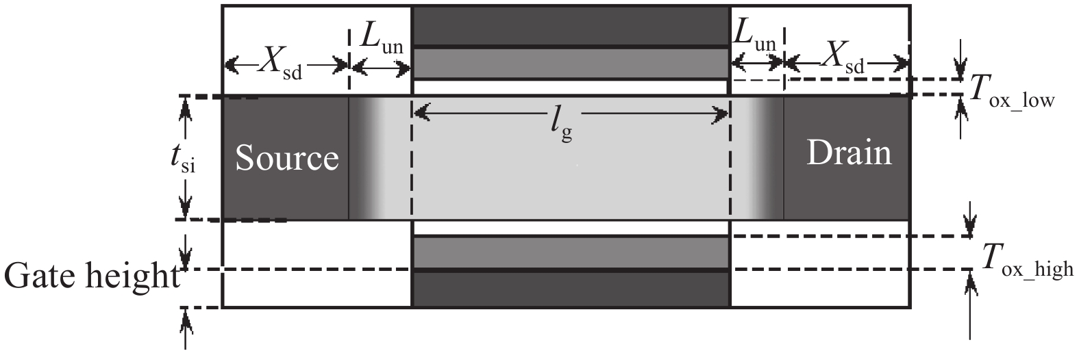
Fig. 1.
Cross-sectional view of 14 nm U-DG-GS NMOSFET.
SEMICONDUCTOR DEVICES
S Chakraborty1, A Dasgupta1, R Das1, , M Kar1, A Kundu1 and C K Sarkar2
Corresponding author: R Das, rahuldas171293@gmail.com
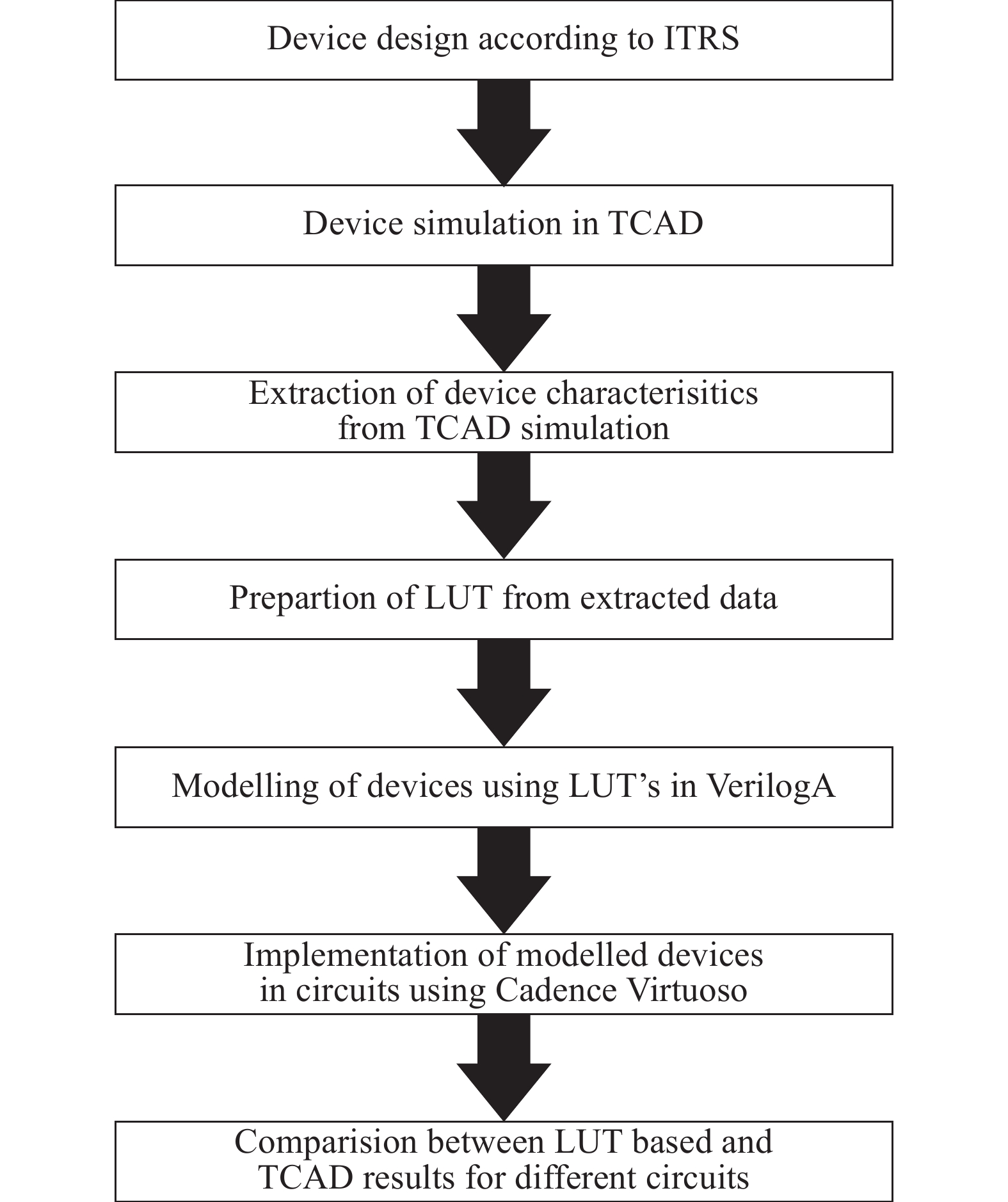
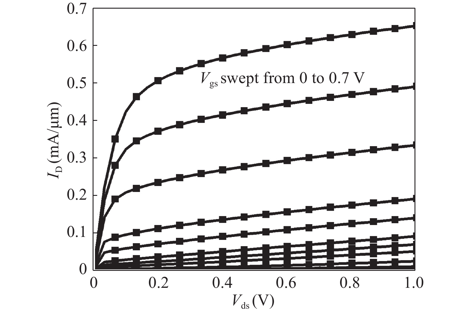
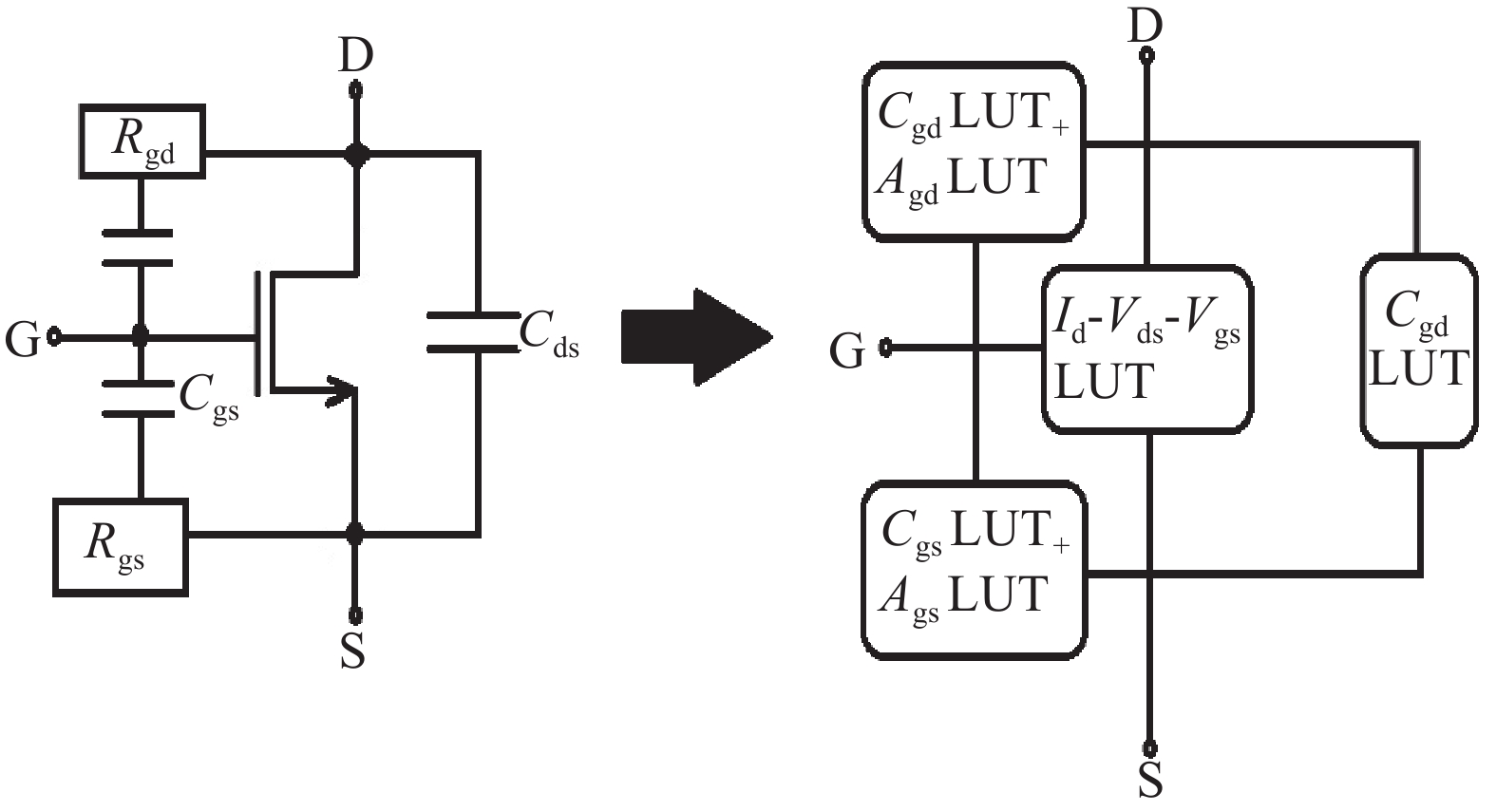
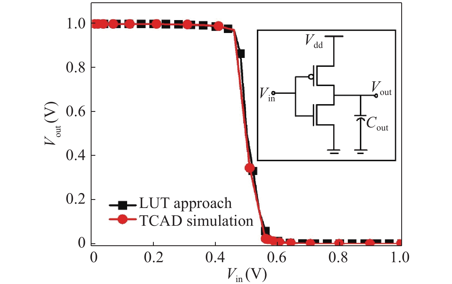
Abstract: In this paper, we explore the possibility of mapping devices designed in TCAD environment to its modeled version developed in cadence virtuoso environment using a look-up table (LUT) approach. Circuit simulation of newly designed devices in TCAD environment is a very slow and tedious process involving complex scripting. Hence, the LUT based modeling approach has been proposed as a faster and easier alternative in cadence environment. The LUTs are prepared by extracting data from the device characteristics obtained from device simulation in TCAD. A comparative study is shown between the TCAD simulation and the LUT-based alternative to showcase the accuracy of modeled devices. Finally the look-up table approach is used to evaluate the performance of circuits implemented using 14 nm nMOSFET.
Key words: 14 nm, double gate MOSFET, look-up table, VerilogA
| [1] |
Xie Q, Xu J, Taur Y. Review and critique of analytic models of MOSFET short-channel effects in subthreshold IEEE Trans Electron Devices, 2012, 59: 1569 doi: 10.1109/TED.2012.2191556
|
| [2] |
Taur Y, Ning T H. Fundamentals of modern VLSI devices. Cambridge University Press, 2009
|
| [3] |
Fossum J G, Chowdhury M M, Trivedi V P, et al. Physical insights on design and modeling of nanoscale FinFETs. IEDM Tech Dig, 2003: 29.1.1
|
| [4] |
Kilchytska V, Nève A, Vancaillie L, et al. Influence of device engineering on the analog and RF performance of SOI MOSFETs. IEEE Trans Electron Devices, 2003, 50(3): 577 doi: 10.1109/TED.2003.810471
|
| [5] |
Trivedi V P, Fossum J G. Nanoscale FinFETs with gate-source/drain underlap. IEEE Trans Electron Devices, 2005, 52(1): 56 doi: 10.1109/TED.2004.841333
|
| [6] |
Deen M J, Marinov O. Effect of forward and reverse substrate biasing on lowfrequency noise in silicon PMOSFETs. IEEE Trans Electron Devices, 2002, 49(3): 409 doi: 10.1109/16.987110
|
| [7] |
Liang X, Taur Y. A 2-D analytical solution for SCEs in DG MOSFETs. IEEE Trans Electron Devices, 2004, 51: 1385 doi: 10.1109/TED.2004.832707
|
| [8] |
Sachid A B, Manoj C R, Sharma D K, et al. Gate fringe-induced barrier lowering in underlap FinFET structures and its optimization. IEEE Electron Device Lett, 2008: 29(1): 128 doi: 10.1109/LED.2007.911974
|
| [9] |
. Bansal A, Paul B C, Roy K. Modeling and optimization of fringe capacitance of nanoscale DGMOS devices. IEEE Trans Electron Devices, 2005, 52(2): 256 doi: 10.1109/TED.2004.842713
|
| [10] |
Paul B C, Bansal A, Roy K. Underlap DGMOS for digital-subthreshold operation. IEEE Trans Electron Devices, 2006, 53: 910 doi: 10.1109/TED.2006.870271
|
| [11] |
Magnone P, Crupi F, Giusi G, et al. 1/f Noise in Drain and Gate Current of MOSFETs With High-k Gate Stacks. IEEE Trans Device Maters Reliab, 2009, 9: 180 doi: 10.1109/TDMR.2009.2020406
|
| [12] |
Houssa M, Pantisano L, Ragnarsson L Å, et al. Electrical properties of high-k gate dielectrics: Challenges, current issues, and possible solutions. Mater Sci Eng, 2006, 51: 37 doi: 10.1016/j.mser.2006.04.001
|
| [13] |
Manoj C R, RamgopalRao V. Impact of High-k Gate Dielectrics on the Device and Circuit Performance of Nanoscale FinFETs. IEEE Electron Device Lett, 2007, 28: 295 doi: 10.1109/LED.2007.892365
|
| [14] |
Zhu W, Han J, Ma T P. Mobility Measurement and Degradation Mechanisms of MOSFETs Made With Ultrathin High-k Dielectrics. IEEE Trans Electron Devices, 2004, 51: 98 doi: 10.1109/TED.2003.821384
|
| [15] |
Kundu A, Dasgupta A, Das R, et al. Influence of underlap on gate stack DG-MOSFET for analytical study of Aanalog/RF performance. Superlattices Microstruct, 2016, 94: 60 doi: 10.1016/j.spmi.2016.04.013
|
| [16] |
International Technology Roadmap for Semiconductor, 2012
|
| [17] |
Sentaurus TCAD Manuals, Synopsys Inc., Mountain View, CA 94043, USA. Release C-2009.06
|
| [18] |
Esseni D, Mastrapasqua M, Celler G K, et al. Low field mobility of ultra-thin SOI N- and P-MOSFETs: measurements and implications on the performance of ultra short MOSFETs. IEEE International Electron Devices Meeting, Technical Digest, 2000: 671
|
| [19] |
Hamed H F, Kaya S, Starzyk J. Compact tunable current-mode analog circuits using DGMOSFETs. IEEE International SOI Conferencee Proceedings, 2006: 69
|


Article views: 4666 Times PDF downloads: 76 Times Cited by: 0 Times
Received: 25 March 2017 Revised: 12 June 2017 Online: Corrected proof: 15 November 2017Published: 01 December 2017
| Citation: |
S Chakraborty, A Dasgupta, R Das, M Kar, A Kundu, C K Sarkar. Device and circuit analysis of a sub 20 nm double gate MOSFET with gate stack using a look-up-table-based approach[J]. Journal of Semiconductors, 2017, 38(12): 124001. doi: 10.1088/1674-4926/38/12/124001
****
S Chakraborty, A Dasgupta, R Das, M Kar, A Kundu, C K Sarkar. Device and circuit analysis of a sub 20 nm double gate MOSFET with gate stack using a look-up-table-based approach[J]. J. Semicond., 2017, 38(12): 124001. doi: 10.1088/1674-4926/38/12/124001.

|
| [1] |
Xie Q, Xu J, Taur Y. Review and critique of analytic models of MOSFET short-channel effects in subthreshold IEEE Trans Electron Devices, 2012, 59: 1569 doi: 10.1109/TED.2012.2191556
|
| [2] |
Taur Y, Ning T H. Fundamentals of modern VLSI devices. Cambridge University Press, 2009
|
| [3] |
Fossum J G, Chowdhury M M, Trivedi V P, et al. Physical insights on design and modeling of nanoscale FinFETs. IEDM Tech Dig, 2003: 29.1.1
|
| [4] |
Kilchytska V, Nève A, Vancaillie L, et al. Influence of device engineering on the analog and RF performance of SOI MOSFETs. IEEE Trans Electron Devices, 2003, 50(3): 577 doi: 10.1109/TED.2003.810471
|
| [5] |
Trivedi V P, Fossum J G. Nanoscale FinFETs with gate-source/drain underlap. IEEE Trans Electron Devices, 2005, 52(1): 56 doi: 10.1109/TED.2004.841333
|
| [6] |
Deen M J, Marinov O. Effect of forward and reverse substrate biasing on lowfrequency noise in silicon PMOSFETs. IEEE Trans Electron Devices, 2002, 49(3): 409 doi: 10.1109/16.987110
|
| [7] |
Liang X, Taur Y. A 2-D analytical solution for SCEs in DG MOSFETs. IEEE Trans Electron Devices, 2004, 51: 1385 doi: 10.1109/TED.2004.832707
|
| [8] |
Sachid A B, Manoj C R, Sharma D K, et al. Gate fringe-induced barrier lowering in underlap FinFET structures and its optimization. IEEE Electron Device Lett, 2008: 29(1): 128 doi: 10.1109/LED.2007.911974
|
| [9] |
. Bansal A, Paul B C, Roy K. Modeling and optimization of fringe capacitance of nanoscale DGMOS devices. IEEE Trans Electron Devices, 2005, 52(2): 256 doi: 10.1109/TED.2004.842713
|
| [10] |
Paul B C, Bansal A, Roy K. Underlap DGMOS for digital-subthreshold operation. IEEE Trans Electron Devices, 2006, 53: 910 doi: 10.1109/TED.2006.870271
|
| [11] |
Magnone P, Crupi F, Giusi G, et al. 1/f Noise in Drain and Gate Current of MOSFETs With High-k Gate Stacks. IEEE Trans Device Maters Reliab, 2009, 9: 180 doi: 10.1109/TDMR.2009.2020406
|
| [12] |
Houssa M, Pantisano L, Ragnarsson L Å, et al. Electrical properties of high-k gate dielectrics: Challenges, current issues, and possible solutions. Mater Sci Eng, 2006, 51: 37 doi: 10.1016/j.mser.2006.04.001
|
| [13] |
Manoj C R, RamgopalRao V. Impact of High-k Gate Dielectrics on the Device and Circuit Performance of Nanoscale FinFETs. IEEE Electron Device Lett, 2007, 28: 295 doi: 10.1109/LED.2007.892365
|
| [14] |
Zhu W, Han J, Ma T P. Mobility Measurement and Degradation Mechanisms of MOSFETs Made With Ultrathin High-k Dielectrics. IEEE Trans Electron Devices, 2004, 51: 98 doi: 10.1109/TED.2003.821384
|
| [15] |
Kundu A, Dasgupta A, Das R, et al. Influence of underlap on gate stack DG-MOSFET for analytical study of Aanalog/RF performance. Superlattices Microstruct, 2016, 94: 60 doi: 10.1016/j.spmi.2016.04.013
|
| [16] |
International Technology Roadmap for Semiconductor, 2012
|
| [17] |
Sentaurus TCAD Manuals, Synopsys Inc., Mountain View, CA 94043, USA. Release C-2009.06
|
| [18] |
Esseni D, Mastrapasqua M, Celler G K, et al. Low field mobility of ultra-thin SOI N- and P-MOSFETs: measurements and implications on the performance of ultra short MOSFETs. IEEE International Electron Devices Meeting, Technical Digest, 2000: 671
|
| [19] |
Hamed H F, Kaya S, Starzyk J. Compact tunable current-mode analog circuits using DGMOSFETs. IEEE International SOI Conferencee Proceedings, 2006: 69
|

 WeChat ID
Journal of Semiconductors © 2017 All Rights Reserved 京ICP备05085259号-2

 DownLoad: