| Citation: |
Guifeng Chen, Mengxue Wang, Wenxian Yang, Ming Tan, Yuanyuan Wu, Pan Dai, Yuyang Huang, Shulong Lu. Optical properties of Zn-diffused InP layers for the planar-type InGaAs/InP photodetectors[J]. Journal of Semiconductors, 2017, 38(12): 124004. doi: 10.1088/1674-4926/38/12/124004
****
G F Chen, M X Wang, W X Yang, M Tan, Y Y Wu, P Dai, Y Y Huang, S L Lu. Optical properties of Zn-diffused InP layers for the planar-type InGaAs/InP photodetectors[J]. J. Semicond., 2017, 38(12): 124004. doi: 10.1088/1674-4926/38/12/124004.
|
Optical properties of Zn-diffused InP layers for the planar-type InGaAs/InP photodetectors
DOI: 10.1088/1674-4926/38/12/124004
More Information
-
Abstract
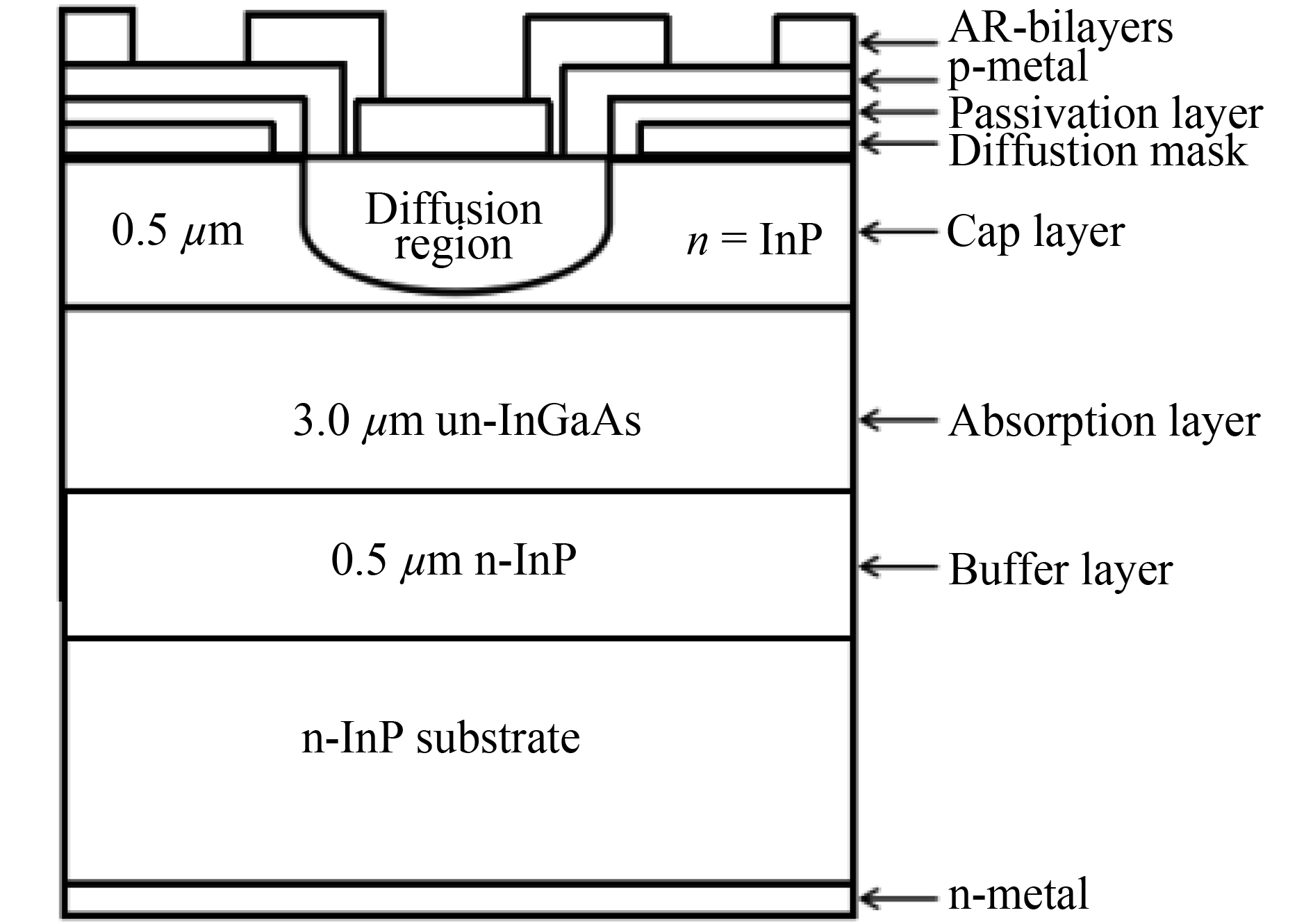
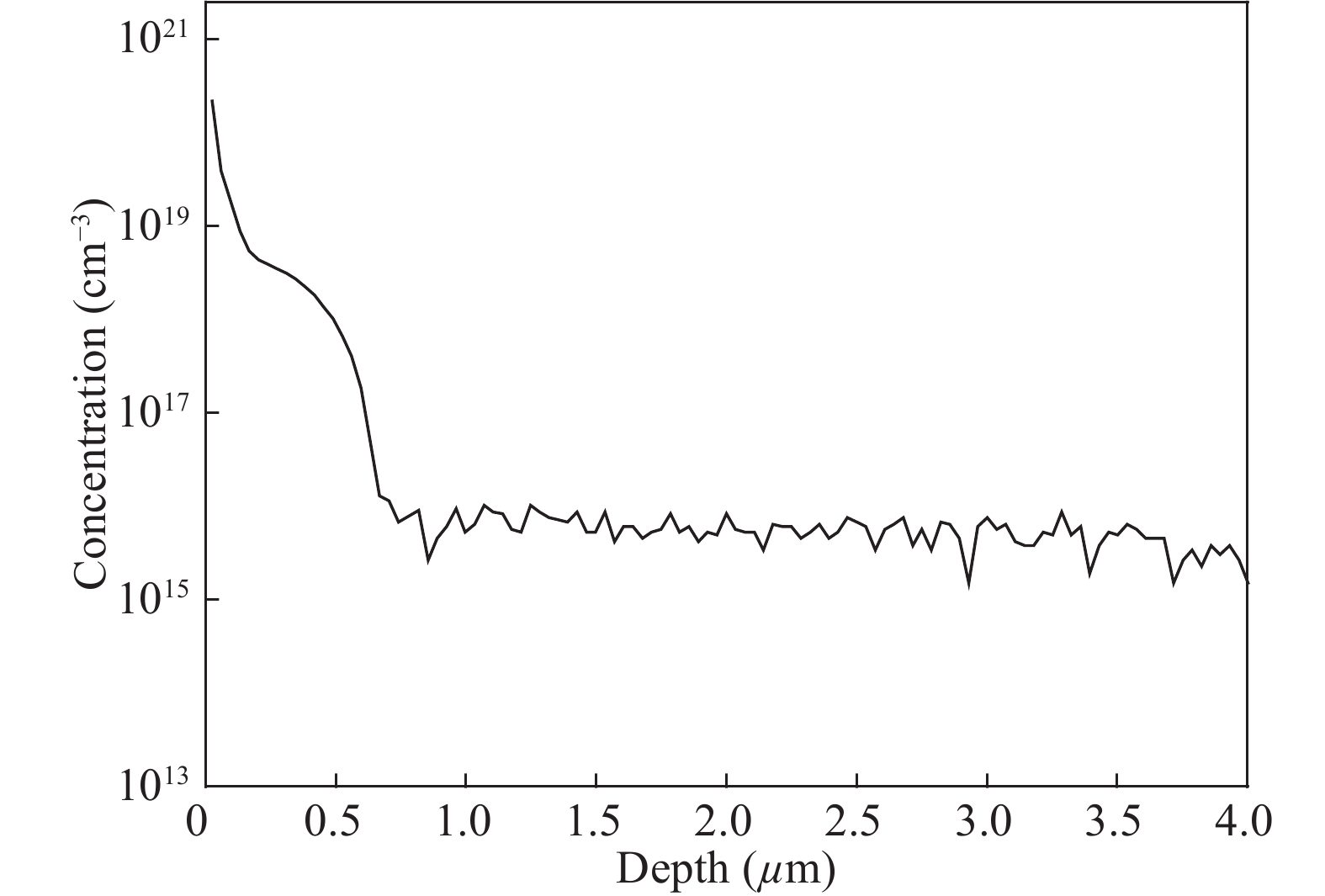
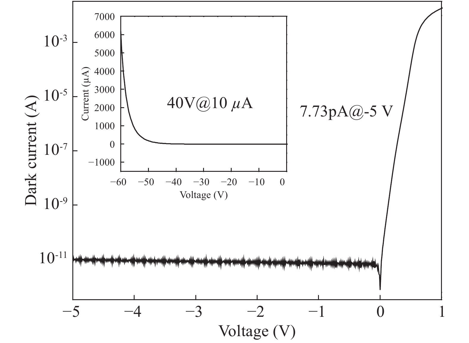
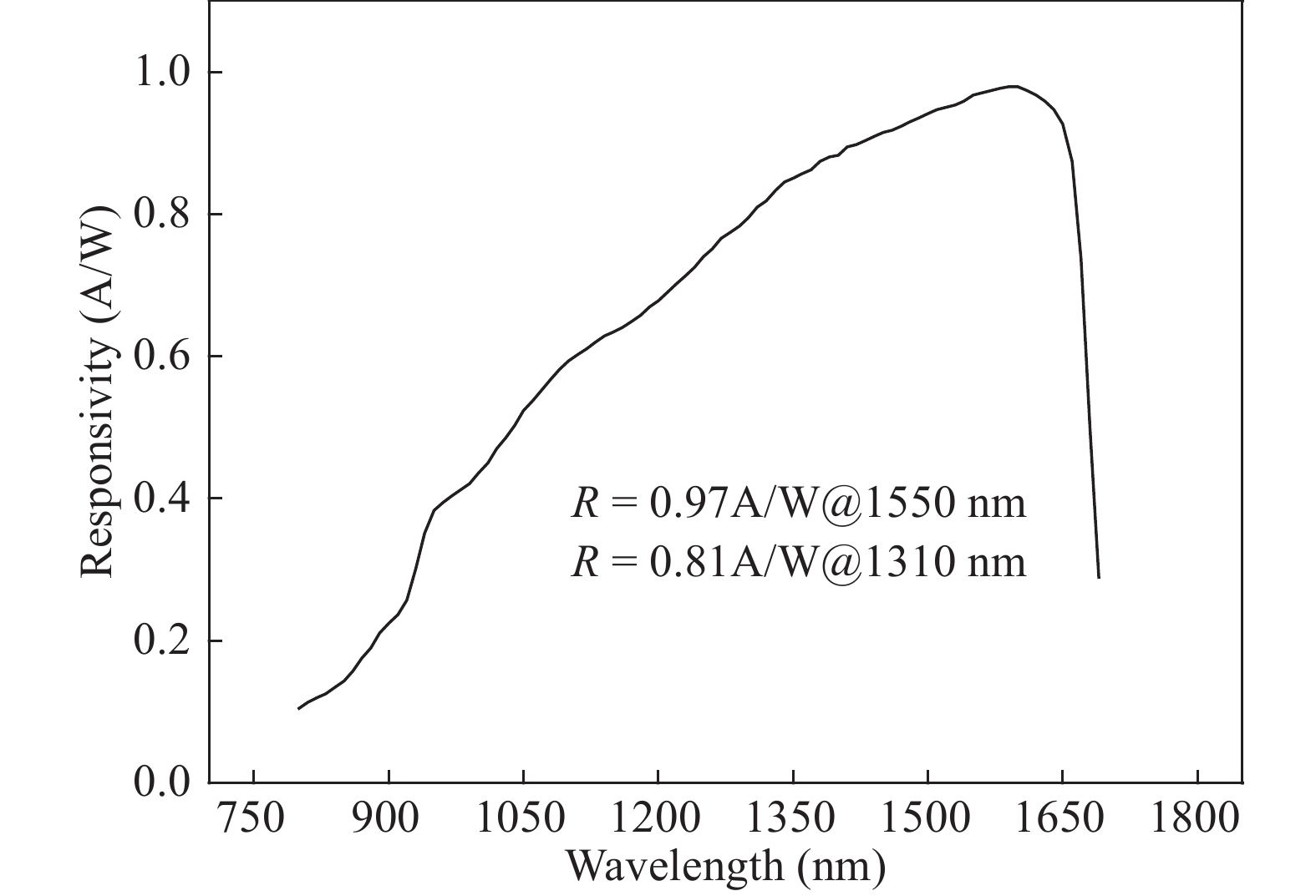
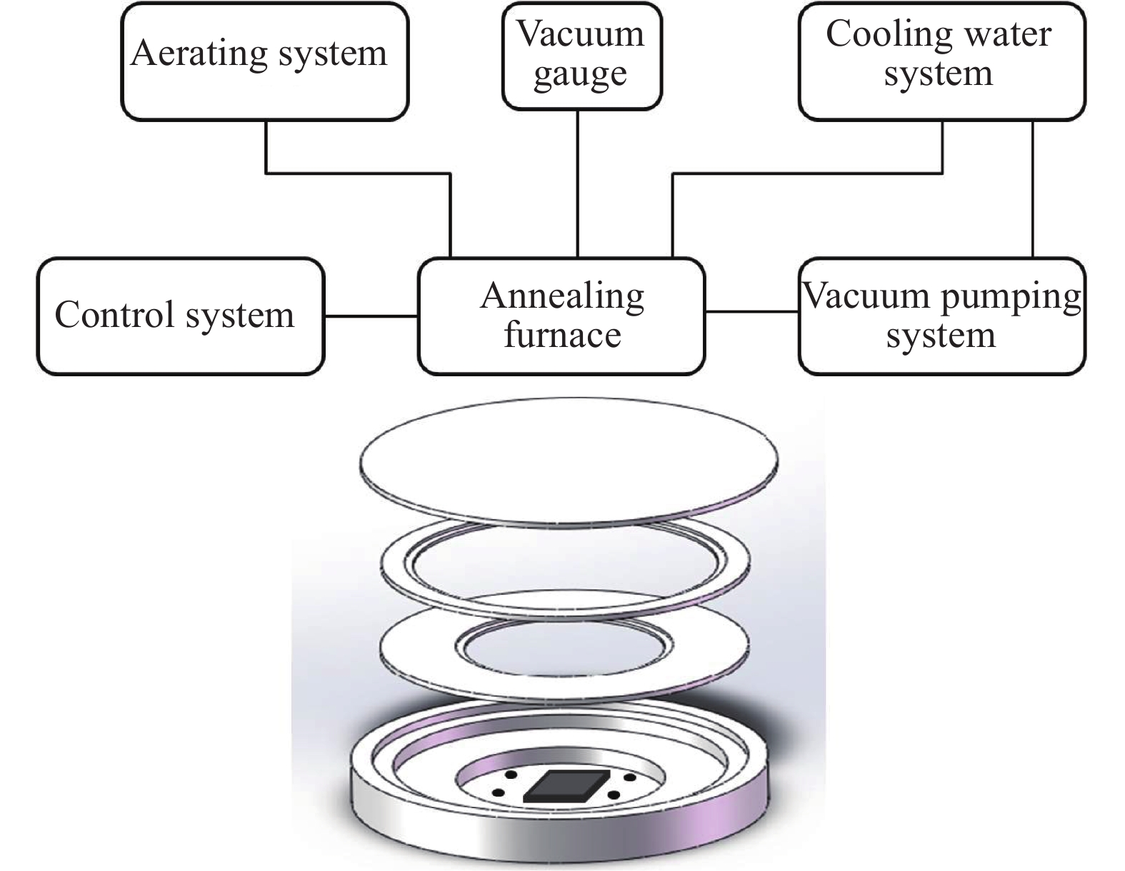
Zn diffusion into InP was carried out ex-situ using a new Zn diffusion technique with zinc phosphorus particles placed around InP materials as zinc source in a semi-closed chamber formed by a modified diffusion furnace. The optical characteristics of the Zn-diffused InP layer for the planar-type InGaAs/InP PIN photodetectors grown by molecular beam epitaxy (MBE) has been investigated by photoluminescence (PL) measurements. The temperature-dependent PL spectrum of Zn-diffused InP samples at different diffusion temperatures showed that band-to-acceptor transition dominates the PL emission, which indicates that Zn was commendably diffused into InP layer as the acceptor. High quality Zn-diffused InP layer with typically smooth surface was obtained at 580 °C for 10 min. Furthermore, more interstitial Zn atoms were activated to act as acceptors after a rapid annealing process. Based on the above Zn-diffusion technique, a 50 μm planar-type InGaAs/InP PIN photodector device was fabricated and exhibited a low dark current of 7.73 pA under a reverse bias potential of −5 V and a high breakdown voltage of larger than 41 V (I < 10 μA). In addition, a high responsivity of 0.81 A/W at 1.31 μm and 0.97 A/W at 1.55 μm was obtained in the developed PIN photodetector. -
References
[1] Jin L F, Zhang Y T, Wang H Y, et al. Accelerated aging of InGaAs PIN photoelectric detectors. Chin J Lasers, 2014, 41(10): 1008002 doi: 10.3788/CJL[2] Yue Z G. Xenics InGaAs SWIR detector is part of Proba-V space mission. Infrares, 2013, 34(7): 19[3] Liu S Q, Han Q, Yang X H, et al. Fabrication and characterization of high-speed and high-efficience photodetector. Laser Optoelectron Prog, 2012, 49(2): 138[4] Dave H, Dewan C, Paul S, et al. AWiFS camera for Resourcesat. Asia-Pacific Remote Sensing Symposium. International Society for Optics and Photonics, 2006: 23[5] Macdougal M H, Geske J C, Wang C, et al. Short-wavelength infrared imaging using low dark current InGaAs detector arrays and vertical-cavity surface-emitting laser illuminators. Mathematics Teacher, 2011, 50(6):1011[6] Wang Y S, Chang S J, Tsai C L, et al. 10-Gb/s planar InGaAs P-I-N photodetectors. IEEE Sens J, 2010, 10(10): 1559 doi: 10.1109/JSEN.2010.2046888[7] Pereira J T, Torres J. Frequency response optimization of dual depletion InGaAs/InP PIN photodiodes. Photonic Sens, 2016, 6(1): 63 doi: 10.1007/s13320-015-0296-2[8] Wang G, Yoneda Y, Aono H, et al. Highly reliable high performance waveguide-integrated InP/InGaAs pin photodiodes for 40 Gbit/s fibre-optical communication application. Electron Lett, 2003, 39(15): 1147 doi: 10.1049/el:20030725[9] Lee Y L, Huang C C, Ho C L, et al. Planar InGaAs p-i-n Photodiodes With Transparent-Conducting-Based Antireflection and Double-Path Reflector. IEEE Electron Device Letters, 2013, 34(11): 1406 doi: 10.1109/LED.2013.2281830[10] Skrimshire C P, Farr J R, Sloan D F, et al. Reliability of mesa and planar InGaAs PIN photodiodes. IEE Proce J Optoelectron, 1990, 137(1): 74 doi: 10.1049/ip-j.1990.0015[11] Ravi M R, Dasgupta A, Dasgupta N. Silicon nitride and polyimide capping layers on InGaAs/InP PIN photodetector after sulfur treatment. J Cryst Growth, 2004, 268(3-4): 359 doi: 10.1016/j.jcrysgro.2004.04.054[12] Chan L Y, Yu K M, Ben-Tzur M, et al. Lattice location of diffused Zn atoms in GaAs and InP single crystals. J Appl Phys, 1991, 69(5): 2998 doi: 10.1063/1.348613[13] Islam M, Feng J Y, Berkovich A, et al. InGaAs/InP PIN photodetector arrays made by MOCVD based zinc diffusion processes. SPIE Defense+Security. 2016: 98190G[14] Ettenberg M H, Lange M J, Sugg A R, et al. Zinc diffusion in InAsP/InGaAs heterostructures. J Electron Mater, 1999, 28(12): 1433 doi: 10.1007/s11664-999-0136-5[15] Wada M, Izumi K, Sakakibara K. Diffusion of zinc acceptors in InAsP by the metal–organic vapor-phase diffusion technique. Appl Phys Lett, 1997, 71(7): 900 doi: 10.1063/1.119682[16] Pitts O J, Hisko M, Benyon W, et al. MOCVD based zinc diffusion process for planar InP/InGaAs avalanche photodiode fabrication. International Conference on Indium Phosphide and Related Materials. 2012: 225[17] Howard A J, Pathangey B, Hayakawa Y, et al. Application of the point-defect analysis technique to zinc doping of MOCVD indium phosphide. Semicond Sci Technol, 2003, 18(8): 723 doi: 10.1088/0268-1242/18/8/301[18] Tang H, Wu X, Zhang K, et al. High uniformity InGaAs linear mesa-type SWIR focal plane arrays. Infrared Mater Devices Appl, 2008, 6835: 683516[19] Kurishima K, Kobayashi T, Ito H, et al. Control of Zn diffusion in InP/InGaAs heterojunction bipolar transistor structures grown by metalorganic vapor phase epitaxy. J Appl Phys, 1996, 79(8): 4017 doi: 10.1063/1.361830[20] Huang C C, Ho C L, Lee Y L, et al. Large-area planar InGaAs p-i-n photodiodes with Mg driven-in by rapid thermal diffusion. IEEE Electron Device Letters, 2014, 35(12): 1278 doi: 10.1109/LED.2014.2362687[21] Huang C C, Ho C L, Wu M C. Large-area planar wavelength-extended InGaAs p–i–n photodiodes by using rapid thermal diffusion with spin-on dopant technique. IEEE Electron Device Lett, 2015, 36(8): 820 doi: 10.1109/LED.2015.2445471[22] Erman M, Gillardin G, Bris J L, et al. Characterization of Fe-doped semi-insulating InP by low temperature and room temperature spatially resolved photoluminescence. J Cryst Growth, 1989, 96(3): 469 doi: 10.1016/0022-0248(89)90041-9[23] Moon Y, Si S, Yoon E, et al. Low temperature photoluminescence characteristics of Zn-doped InP grown by metalorganic chemical vapor deposition. J Appl Phys, 1998, 83(4): 2261 doi: 10.1063/1.366966[24] Dingle R. Luminescent transitions associated with divalent copper impurities and the green emission from semiconducting zinc oxide. Phys Rev Lett, 1969, 23(11): 579 doi: 10.1103/PhysRevLett.23.579[25] Kim T S, Lester S D, Streetman B G. Studies of the 1.35-eV photoluminescence band in InP. J Appl Phys, 1987, 62(4): 1363 doi: 10.1063/1.339639[26] Temkin H, Dutt B V, Bonner W A. Photoluminescence study of native defects in InP. Appl Phys Lett, 1981, 38(6): 431 doi: 10.1063/1.92386[27] Hsu J K, Juang C, Lee B J, et al. Photoluminescence studies of interstitial Zn in InP due to rapid thermal annealing. J Vac Sci Technol B, 1994, 12(3): 1416 doi: 10.1116/1.587310[28] Montie E A, Gurp G J V. Photoluminescence of Zn-diffused and annealed InP. J Appl Phys, 1989, 66(11): 5549 doi: 10.1063/1.343659[29] Wong C D, Bube R H. Bulk and surface effects of heat treatment of p-type InP crystals. J Appl Phys, 1984, 55(10): 3804 doi: 10.1063/1.332889[30] Hess K, Stath N, Benz K W. Liquid phase epitaxy of InP. J Electrocheml Soc, 1974, 121(9): 1208 doi: 10.1149/1.2402014[31] Kubota E, Ohmori Y, Sugii K. Electrical and optical properties of Mg–, Ca–, and Zn– doped InP crystals grown by the synthesis, solute diffusion technique. J Appl Phys, 1984, 55(10): 3779 doi: 10.1063/1.332934[32] Yoon K H, Lee Y H, Yeo D H, et al. The characteristics of Zn-doped InP using spin-on dopant as a diffusion source. Journal of Electronic Materials, 2002, 31(4): 244 doi: 10.1007/s11664-002-0139-y[33] Borghesi A, Guizzetti G, Patrini M, et al. Infrared study and characterization of Zn diffused InP. J Appl Phys, 1993, 74(4): 2445 doi: 10.1063/1.354681[34] Ishikawa T, Inata T, Kondo K, et al. Annealing effect in Si-doped GaAs and AlGaAs layers grown by MBE. Electron Lett, 1986, 22(4): 189 doi: 10.1049/el:19860132 -
Proportional views


 DownLoad:
