| [1] |
Schaller R. Moore's law: past, present and future. IEEE Spectrum, 1997, 34(6), 52 doi: 10.1109/6.591665 |
| [2] |
Frank D J, Dennard R H, Nowak E, et al. Device scaling limits of Si MOSFETs and their application dependencies. Proc IEEE, 2001, 89(3), 259 doi: 10.1109/5.915374 |
| [3] |
Sarkar D, Xie X J, Liu W, et al. A subthermionic tunnel field-effect transistor with an atomically thin channel. Nature, 2015, 526, 91 doi: 10.1038/nature15387 |
| [4] |
Arnold A J, Razavieh A, Nas J R, et al. Mimicking neurotransmitter release in chemical synapses via hysteresis engineering in MoS 2 transistors. ACS Nano, 2017, 11(3), 3110 doi: 10.1021/acsnano.7b00113 |
| [5] |
Gong Y J, Shi G, Zhang Z H, et al. Direct chemical conversion of graphene to boronand nitrogen-and carbon-containing atomic layers. Nat Common, 2014, 5, 3193 doi: 10.1038/ncomms4193 |
| [6] |
Xie Y L, Lian B, Jäck B, et al. Spectroscopic signatures of many-body correlations in magic-angle twisted bilayer graphene. Nature, 2019, 572, 101 doi: 10.1038/s41586-019-1422-x |
| [7] |
Li L F, Liu W, Gao A Y, et al. Plasmon excited ultrahot carriers and negative differential photoresponse in a vertical graphene van der Waals heterostructure. Nano Lett, 2019, 19(5), 3295 doi: 10.1021/acs.nanolett.9b00908 |
| [8] |
Novoselov K S, Geim A K, Morozov S V, et al. Two-dimensional gas of massless Dirac fermions in graphene. Nature, 2005, 438, 197 doi: 10.1038/nature04233 |
| [9] |
Zhang Y B, Tan Y W, Stormer H L, et al. Experimental observation of the quantum Hall effect and Berry's phase in graphene. Nature, 2005, 438, 201 doi: 10.1038/nature04235 |
| [10] |
Lee C, Wei X D, Kysar J W, et al. Measurement of the elastic properties and intrinsic strength of monolayer graphene. Science, 2008, 321(5887), 385 doi: 10.1126/science.1157996 |
| [11] |
Liu Y P, Yudhistira I, Yang M, et al. Phonon-mediated colossal magnetoresistance in graphene/black phosphorus heterostructures. Nano Lett, 2018, 18(6), 3377 doi: 10.1021/acs.nanolett.8b00155 |
| [12] |
Huang S Y, Zhang G W, Fan F R, et al. Strain-tunable van der Waals interactions in few-layer black phosphorus. Nat Common, 2019, 10, 2447 doi: 10.1038/s41467-019-10483-8 |
| [13] |
Chaudhary K, Tamagnone M, Rezaee M, et al. Engineering phonon polaritons in van der Waals heterostructures to enhance in-plane optical anisotropy. Sci Adv, 2019, 5(4), eaau7171 doi: 10.1126/sciadv.aau7171 |
| [14] |
Kim J M, Baik S S, Ryu S H, et al. Observation of tunable band gap and anisotropic Dirac semimetal state in black phosphorus. Science, 2015, 349(6249), 723 doi: 10.1126/science.aaa6486 |
| [15] |
Peng R M, Khaliji K, Youngblood N, et al. Midinfrared electro-optic modulation in few-layer black phosphorus. Nano Lett, 2017, 17(10), 6315 doi: 10.1021/acs.nanolett.7b03050 |
| [16] |
Liu Z, Gong Y G, Zhou W, et al. Ultrathin high-temperature oxidation-resistant coatings of hexagonal boron nitride. Nat Commun, 2013, 4, 2541 doi: 10.1038/ncomms3541 |
| [17] |
Wu E X, Xie Y, Zhang J, et al. Dynamically controllable polarity modulation of MoTe 2 field-effect transistors through ultraviolet light and electrostatic activation. Sci Adv, 2019, 5(5), eaav3430 doi: 10.1126/sciadv.aav3430 |
| [18] |
Park H J, Tay R Y J, Wang X, et al. Double-spiral hexagonal boron nitride and shear strained coalescence boundary. Nano Lett, 2019, 19(7), 4229 doi: 10.1021/acs.nanolett.8b05034 |
| [19] |
Song L, Ci L J, Lu H, et al. Large scale growth and characterization of atomic hexagonal boron nitride layers. Nano Lett, 2010, 10(8), 3209 doi: 10.1021/nl1022139 |
| [20] |
Ci L J, Song L, Jin C J, et al. Atomic layers of hybridized boron nitride and graphene domains. Nat Mater, 2010, 9, 430 doi: 10.1038/nmat2711 |
| [21] |
Gong Y G, Lin J H, Wang X L, et al. Vertical and in-plane heterostructures from WS 2/MoS 2 monolayers. Nat Mater, 2014, 13, 1135 doi: 10.1038/nmat4091 |
| [22] |
Gong Y G, Liu Z, Lupini A R, et al. Band gap engineering and layer-by-layer mapping of selenium doped molybdenum disulfide. Nano Lett, 2014, 14(2), 442 doi: 10.1021/nl4032296 |
| [23] |
Ma Y, Ajayan P M, Gong Y J, et al. Recent advances in synthesis and applications of 2D junctions. Small, 2018, 14(38), 1801606 doi: 10.1002/smll.201801606 |
| [24] |
Lin Y C, Li S S, Komsa H P, et al. Revealing the atomic defects of WS 2 governing its distinct optical emissions. Adv Funct Mater, 2017, 28(4), 1704210 doi: 10.1002/adfm.201704210 |
| [25] |
Sun L F, Leong W S, Yang S Z, et al. Concurrent synthesis of high-performance monolayer transition metal disulfdes. Adv Funct Mater, 2017, 27(15), 1605896 doi: 10.1002/adfm.201605896 |
| [26] |
Zhou Y, Jang H J, Woods J M, et al. Direct synthesis of large-scale WTe 2 thin films with low thermal conductivity. Adv Funct Mater, 2017, 27(8), 1605928 doi: 10.1002/adfm.201605928 |
| [27] |
Zhao Y D, Qiao J S, Yu P, et al. Extraordinarily strong interlayer interaction in 2D layered PtS 2. Adv Mater, 2017, 28(12), 2399 doi: 10.1002/adma.201504572 |
| [28] |
Wu J X, Liu Y J, Tan Z J, et al. Chemical patterning of high-mobility semiconducting 2D Bi 2O 2Se crystals for integrated optoelectronic devices. Adv Mater, 2017, 29(44), 1704060 doi: 10.1002/adma.201704060 |
| [29] |
Li L, Guo Y C, Sun Y P, et al. A general method for the chemical synthesis of large-scale, seamless transition metal dichalcogenide electronics. Adv Mater, 2018, 30(12), 1706215 doi: 10.1002/adma.201706215 |
| [30] |
Huan Y H, Shi J P, Zou X L, et al. Vertical 1T-TaS 2 synthesis on nanoporous gold for high-performance electrocatalytic applications. Adv Mater, 2018, 30(15), 1705916 doi: 10.1002/adma.201705916 |
| [31] |
Zhang T, Fu L. Controllable chemical vapor deposition growth of two-dimensional heterostructures. Chem, 2018, 4(4), 671 doi: 10.1016/j.chempr.2017.12.006 |
| [32] |
Xu R J, Jang H, Lee M H, et al. Vertical MoS 2 double-layer memristor with electrochemical metallization as an atomic-scale synapse with switching thresholds approaching 100 mV. Nano Lett, 2019, 19(4), 2411 doi: 10.1021/acs.nanolett.8b05140 |
| [33] |
Zhu Y B, Li Y J, Arefe R A, et al. Monolayer molybdenum disulfide transistors with single-atomthick gates. Nano Lett, 2018, 18(6), 3807 doi: 10.1021/acs.nanolett.8b01091 |
| [34] |
Kim S, Yao Z P, Lim J M, et al. Atomic-scale observation of electrochemically reversible phase transformations in SnSe 2 single crystals. Adv Mater, 2018, 30(51), 1804925 doi: 10.1002/adma.201804925 |
| [35] |
Liu C S, Yan X, Song X F, et al. A semi-floating gate memory based on van der Waals heterostructures for quasi-non-volatile applications. Nat Nano, 2018, 13, 404 doi: 10.1038/s41565-018-0102-6 |
| [36] |
Gao A Y, Lai J W, Wang Y J, et al. Observation of ballistic avalanche phenomena in nanoscale vertical InSe/BP heterostructures. Nat Nano, 2019, 14, 217 doi: 10.1038/s41565-018-0348-z |
| [37] |
Das S, Robinson J A, Dubey M, et al. Beyond graphene: progress in novel two dimensional materials and van der Waals solids. Annu Rev Mater Res, 2015, 45, 1 doi: 10.1146/annurev-matsci-070214-021034 |
| [38] |
Sangwan V K, Beck M E, Henning A, et al. Self-aligned van der Waals heterojunction diodes and transistors. Nano Lett, 2018, 18(2), 1421 doi: 10.1021/acs.nanolett.7b05177 |
| [39] |
Lembke D, Kis A. Breakdown of high-performance monolayer MoS 2 transistors. ACS Nano, 2012, 6(11), 10070 doi: 10.1021/nn303772b |
| [40] |
Manzeli S, Ovchinnikov D, Pasquier D, et al. 2D transition metal dichalcogenides. Nat Rev Mater, 2017, 2, 17033 doi: 10.1038/natrevmats.2017.33 |
| [41] |
Luo W, Zhu M J, Peng G, et al. Carrier modulation of ambipolar few-layer MoTe 2 transistors by MgO surface charge transfer doping. Adv Mater, 2018, 28(15), 1704539 doi: 10.1002/adfm.201704539 |
| [42] |
Avsar A, Marinov K, Marin E G, et al. Reconfgurable diodes based on vertical WSe 2 transistors with van der Waals bonded contacts. Adv Mater, 2018, 30(18), 17072000 doi: 10.1002/adma.201707200 |
| [43] |
Kim S, Maassen J, Lee J, et al. Interstitial Mo-assisted photovoltaic effect in multilayer MoSe 2 phototransistors. Adv Mater, 2018, 30(12), 1705542 doi: 10.1002/adma.201705542 |
| [44] |
Song S H, Joo M K, Neumann M, et al. Probing defect dynamics in monolayer MoS 2 via noise nanospectroscopy. Nat Commun, 2017, 8, 2121 doi: 10.1038/s41467-017-02297-3 |
| [45] |
Tian H, Guo Q S, Xie Y J, et al. Anisotropic black phosphorus synaptic device for neuromorphic applications. Adv Mater, 2016, 28(25), 4991 doi: 10.1002/adma.201600166 |
| [46] |
Jena D, Banerjee K, Xing G H, et al. 2D crystal semiconductors: Intimate contacts. Nat Mater, 2014, 13, 2640 doi: 10.1038/nmat4121 |
| [47] |
Xu L P, Zhang P, Jiang H N, et al. Large-scale growth and field-effect transistors electrical engineering of atomic-layer SnS 2. Small, 2019, 15(46), 1904116 doi: 10.1002/smll.201904116 |
| [48] |
Han G H, Duong D L, Keum D H, et al. Van der Waals metallic transition metal dichalcogenides. Chem Rev, 2018, 118(13), 6297 doi: 10.1021/acs.chemrev.7b00618 |
| [49] |
Schulman D S, Arnold A J, Das S. Contact engineering for 2D materials and devices. Chem Soc Rev, 2018, 47(9), 3037 doi: 10.1039/C7CS00828G |
| [50] |
Baranowski M, Surrente A, Klopotowski L, et al. Probing the interlayer exciton physics in a MoS 2/MoSe 2/MoS 2 van der Waals heterostructure. Nano Lett, 2017, 17(10), 6360 doi: 10.1021/acs.nanolett.7b03184 |
| [51] |
Islam M A, Kim J H, Schropp A, et al. Centimeter-scale 2D van der Waals vertical heterostructures integrated on deformable substrates enabled by gold sacrificial layer-assisted growth. Nano Lett, 2017, 17(10), 6157 doi: 10.1021/acs.nanolett.7b02776 |
| [52] |
Yan C Y, Gong C H, Wang P H, et al. 2D group IVB transition metal dichalcogenides. Adv Funct Mater, 2018, 28(39), 1803305 doi: 10.1002/adfm.201803305 |
| [53] |
Voiry D, Mohite A, Chhowalla M. Phase engineering of transition metal dichalcogenides. Chem Soc Rev, 2015, 44, 2702 doi: 10.1039/C5CS00151J |
| [54] |
Wang X S, Song Z G, Wen W, et al. Potential 2D materials with phase transitions: structure, synthesis, and device applications. Adv Mater, 2019, 31(45), 1804682 doi: 10.1002/adma.201804682 |
| [55] |
Stark M S, Kuntz K L, Martens S J, et al. Intercalation of layered materials from bulk to 2D. Adv Mater, 2019, 31(27), 1808213 doi: 10.1002/adma.201808213 |
| [56] |
Li H, Ruan S C, Zeng Y J. Intrinsic van der Waals magnetic materials from bulk to the 2D limit: new frontiers of spintronics. Adv Mater, 2019, 31(27), 1900065 doi: 10.1002/adma.201900065 |
| [57] |
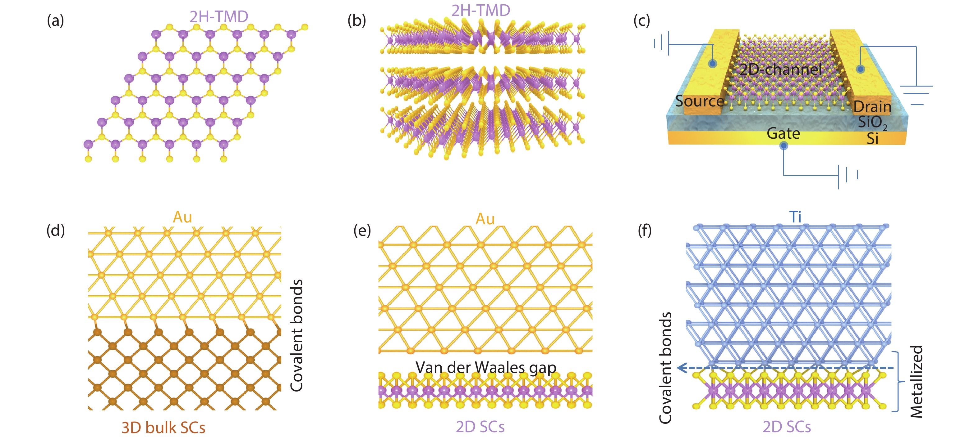
Allain A, Kang J H, Banerjee K, et al. Electrical contacts to two-dimensional semiconductors. Nat Mater, 2015, 14, 1195 doi: 10.1038/nmat4452 |
| [58] |
Kang J, Liu W, Sarkar D. Computational study of metal contacts to monolayer transitionmetal dichalcogenide semiconductors. Phys Rev X, 2014, 4(3), 031005 doi: 10.1103/PhysRevX.4.031005 |
| [59] |
Ranuárez J C, Deen M J, Chen C H. A review of gate tunneling current in MOS devices. Microelectron Reliab, 2016, 46(12), 1939 doi: 10.1016/j.microrel.2005.12.006 |
| [60] |
Liu Y, Guo J, Zhu E B, et al. Approaching the Schottky–Mott limit in van der Waals metal–semiconductor junctions. Nature, 2018, 557, 696 doi: 10.1038/s41586-018-0129-8 |
| [61] |
English C D, Shine G, Dorgan V E, et al. Improved contacts to MoS 2 transistors by ultra-high vacuum metal deposition. Nano Lett, 2016, 16(6), 3824 doi: 10.1021/acs.nanolett.6b01309 |
| [62] |
Stokbro K, Engelund M, Blom A. Atomicscale model for the contact resistance of the nickelgraphene interface. Phys Rev B, 2012, 85(16), 165442 doi: 10.1103/PhysRevB.85.165442 |
| [63] |
Popov I, Seifert G, Tománek D. Designing electrical contacts to MoS 2 monolayers: a computational study. Phys Rev Lett, 2012, 108(15), 156802 doi: 10.1103/PhysRevLett.108.156802 |
| [64] |
Liu W, Kang J H, Cao W, et al. High performance few layer MoS 2 field-effect-transistor with record low contactresistance. IEEE Int Electron Devices Meet, 2013, 19.4. 1 doi: 10.1109/IEDM.2013.6724660 |
| [65] |
Wang L, Meric I, Huang P Y, et al. One-dimensional electrical contact to a two-dimensional material. Science, 2013, 342(6158), 614 doi: 10.1126/science.1244358 |
| [66] |
Cui X, Lee G H, Kim Y D, et al. Multi-terminal transport measurements of MoS 2 using a van der Waals heterostructure device platform. Nat Mater, 2015, 10, 534 doi: 10.1038/nnano.2015.70 |
| [67] |
Chai Y, Ionescu R, Su S S, et al. Making one-dimensional electrical contacts to molybdenum disulfid-based heterostructures through plasma etching. Phys Status Solidi A, 2016, 213(5), 1358 doi: 10.1002/pssa.201532799 |
| [68] |
Matsuda Y, Deng W Q, Goddard W A. Contact resistance for “end-contacted” metal−graphene and metal−nanotube interfaces from quantum mechanics. J Phys Chem C, 2010, 114(41), 17845 doi: 10.1021/jp806437y |
| [69] |
Karpiak B, Dankert A, Cummings A W, et al. 1D ferromagnetic edge contacts to 2D graphene/h-BN heterostructures. 2D Mater, 2017, 5(1), 014001 doi: 10.1088/2053-1583/aa8d2b |
| [70] |
Zhang Y, Yin L, Chu J W, et al. Edge-epitaxial growth of 2D NbS 2-WS 2 lateral metal-semiconductor heterostructures. Adv Mater, 2018, 30(40), 1803665 doi: 10.1002/adma.201803665 |
| [71] |
Gong Y J, Lei S D, Ye G L, et al. Two-step growth of two-dimensional WSe 2/MoSe 2 heterostructures. Nano Lett, 2015, 15(9), 6135 doi: 10.1021/acs.nanolett.5b02423 |
| [72] |
Gong Y G, Lin Z, Ye G L, et al. Tellurium-assisted low-temperature synthesis of MoS 2 and WS 2 monolayers. ACS Nano, 2015, 9(12), 11658 doi: 10.1021/acsnano.5b05594 |
| [73] |
Ji Q Q, Li C, Wang J L, et al. Metallic vanadium disulfide nanosheets as a platform material for multifunctional electrode applications. Nano Lett, 2017, 17(8), 4908 doi: 10.1021/acs.nanolett.7b01914 |
| [74] |
Zhou J D, Lin J H, Huang X W, et al. A library of atomically thin metal chalcogenides. Nature, 2018, 556, 358 doi: 10.1038/s41586-018-0008-3 |
| [75] |
Leong W S, Ji Q Q, Mao N N, et al. Synthetic lateral metal–semiconductor heterostructures of transition metal disulfides. J Am Chem Soc, 2018, 140(39), 12354 doi: 10.1021/jacs.8b07806 |
| [76] |
Lee C S, Oh S J, Heo H, et al. Epitaxial van der Waals contacts between transition-metal dichalcogenide monolayer polymorphs. Nano Lett, 2019, 19(3), 1814 doi: 10.1021/acs.nanolett.8b04869 |
| [77] |
Wu R X, Tao Q Y, Dang W Q, et al. van der Waals epitaxial growth of atomically thin 2D metals on dangling-bond-free WSe 2 and WS 2. Adv Funct Mater, 2019, 29(12), 1806611 doi: 10.1002/adfm.201806611 |
| [78] |
Jin Y Y, Zeng Z Y, Xu Z W, et al. Synthesis and transport properties of degenerate p-type Nb-doped WS 2 monolayers. Chem Mater, 2019, 31(9), 3534 doi: 10.1021/acs.chemmater.9b00913 |
| [79] |
Suh J, Park T E, Lin D Y, et al. Doping against the native propensity of MoS 2: degenerate hole doping by cation substitution. Nano Lett, 2014, 14(12), 6976 doi: 10.1021/nl503251h |
| [80] |
Kappera R, Voiry D, Yalcin S E, et al. Phase-engineered low-resistance contacts for ultrathin MoS 2 transistors. Nat Mater, 2014, 13, 1128 doi: 10.1038/nmat4080 |
| [81] |
Zhu J Q, Wang Z G, Yu H, et al. Argon plasma induced phase transition in monolayer MoS 2. J Am Chem Soc, 2017, 139(30), 10216 doi: 10.1021/jacs.7b05765 |
| [82] |
Gong Y J, Yuan H T, Wu C L, et al. Spatially controlled doping of two-dimensional SnS 2 through intercalation for electronics. Nat Nano, 2018, 13, 294 doi: 10.1038/s41565-018-0069-3 |
| [83] |
Schottky W. Zur Halbleitertheorie der sperrschicht-und spitzengleichrichter. Z Phys A, 1939, 113, 367 doi: 10.1007/BF01340116 |
| [84] |
|
| [85] |
Bardeen J. Surface states and rectifcation at a metal semi-conductor contact. Phys Rev, 1947, 71, 717 doi: 10.1103/PhysRev.71.717 |
| [86] |
Das S, Chen H Y, Penumatcha A V, et al. High performance multi-layer MoS 2 transistors with scandium contacts. Nano Lett, 2013, 13(1), 100 doi: 10.1021/nl303583v |
| [87] |
Wang Y, Kim J C, Wu R J, et al. Van der Waals contacts between three-dimensional metals and two-dimensional semiconductors. Nature, 2019, 568, 70 doi: 10.1038/s41586-019-1052-3 |
| [88] |
Kang J, Sarkar D, Liu W, et al. A computational study of metalcontacts to beyondgraphene 2D semiconductor materials. IEEE Int Electron Devices Meet, 2012, 407
|
| [89] |
Khatami Y, Li H, Xu C, et al. Metal-to-multilayer-graphene contact—Part II: analysis of contact resistance. IEEE Trans Electron Devices, 2012, 59, 2453 doi: 10.1109/TED.2012.2205257 |
| [90] |
Khatami Y, Li H, Xu C, et al. Metal-to-multilayer-graphene contact—Part I: contact resistance modeling. IEEE Trans Electron Devices, 2012, 59, 2444 doi: 10.1109/TED.2012.2205256 |
| [91] |
Zhao M, Ye Y, Han Y, et al. Large-scale chemical assembly of atomically thin transistors and circuits. Nat Nano, 2016, 11, 954 doi: 10.1038/nnano.2016.115 |
| [92] |
Hong W, Shim G W, Yang S Y, et al. Improved electrical contact properties of MoS 2-graphene lateral heterostructure. Adv Funct Mater, 2019, 29(6), 1807550 doi: 10.1002/adfm.201807550 |
| [93] |
Leong W S, Nai C T, Tong J T L. What does annealing do to metal-graphene contacts. Nano Lett, 2014, 14(7), 3840 doi: 10.1021/nl500999r |
| [94] |
Léonard F, Talin A A. Electrical contacts to one- and two-dimensional nanomaterials. Nat Nano, 2011, 6, 773 doi: 10.1038/nnano.2011.196 |
| [95] |
|
| [96] |
Liu L N, Wu J X, Wu L Y, et al. Phase-selective synthesis of 1T’ MoS 2 monolayers and heterophase bilayers. Nat Mater, 2018, 17, 1108 doi: 10.1038/s41563-018-0187-1 |
| [97] |
Zheng J Y, Yan X X, Lu Z X, et al. High-mobility multilayered MoS 2 flakes with low contact resistance grown by chemical vapor deposition. Adv Mater, 2017, 29(13), 1604540 doi: 10.1002/adma.201604540 |
| [98] |
Gong C, Colombo L, Wallace R M, et al. The unusual mechanism of partial fermi level pinning at metal –MoS 2 interfaces. Nano Lett, 2014, 14(4), 1714 doi: 10.1021/nl403465v |
| [99] |
Saidi W A. Trends in the adsorption and growth morphology of metals on the MoS 2 (001) surface. Cryst Growth Des, 2015, 15(7), 3190 doi: 10.1021/acs.cgd.5b00269 |
| [100] |
Meng L J, Ma Y, Si K P, et al. Recent advances of phase engineering in group VI transition metal dichalcogenides. Tungsten, 2019, 1, 46 doi: 10.1007/s42864-019-00012-x |
| [101] |
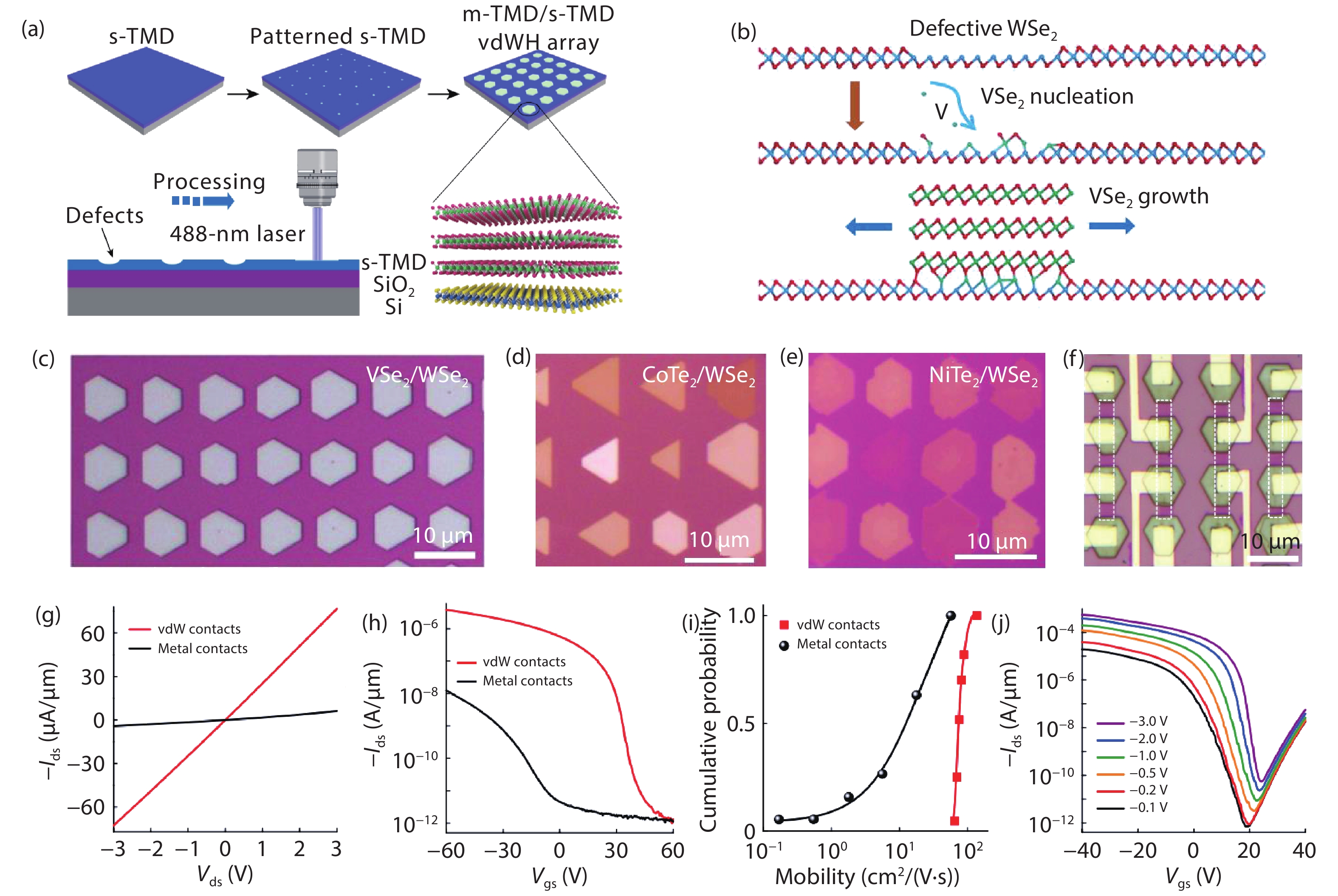
Li J, Yang X D, Liu Y, et al. General synthesis of two-dimensional van der Waals heterostructure arrays. Nature, 2020, 579, 368 doi: 10.1038/s41586-020-2098-y |


 DownLoad: