Issue Browser
Volume 41, Issue 7,
Jul 2020
Column
J. Semicond.
2020, 41(7): 071901 doi: 10.1088/1674-4926/41/7/071901
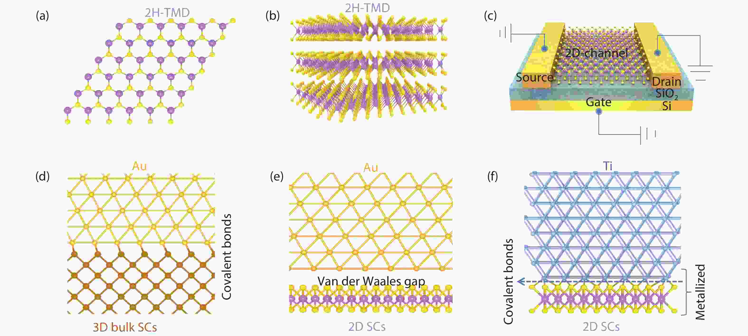
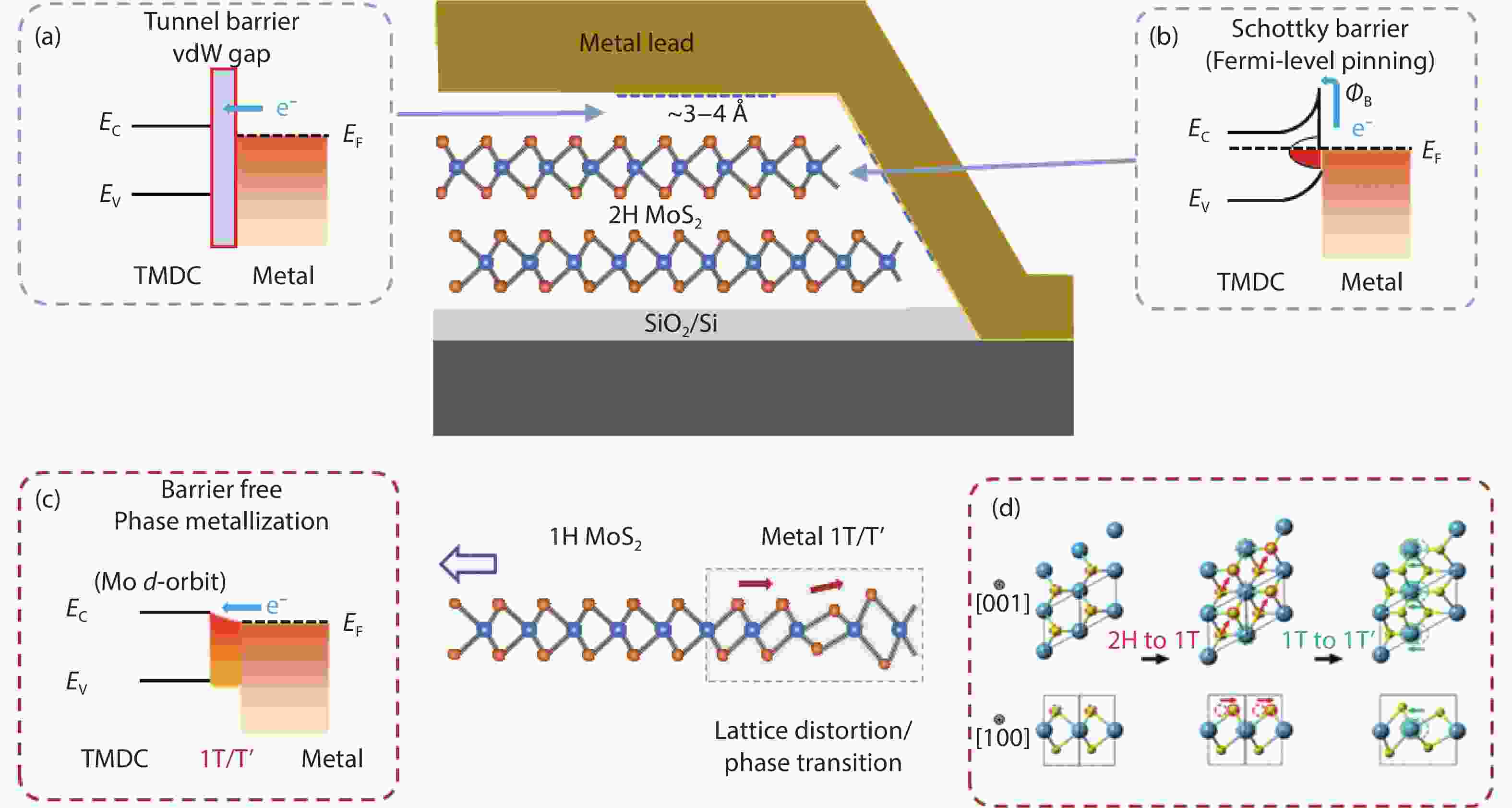
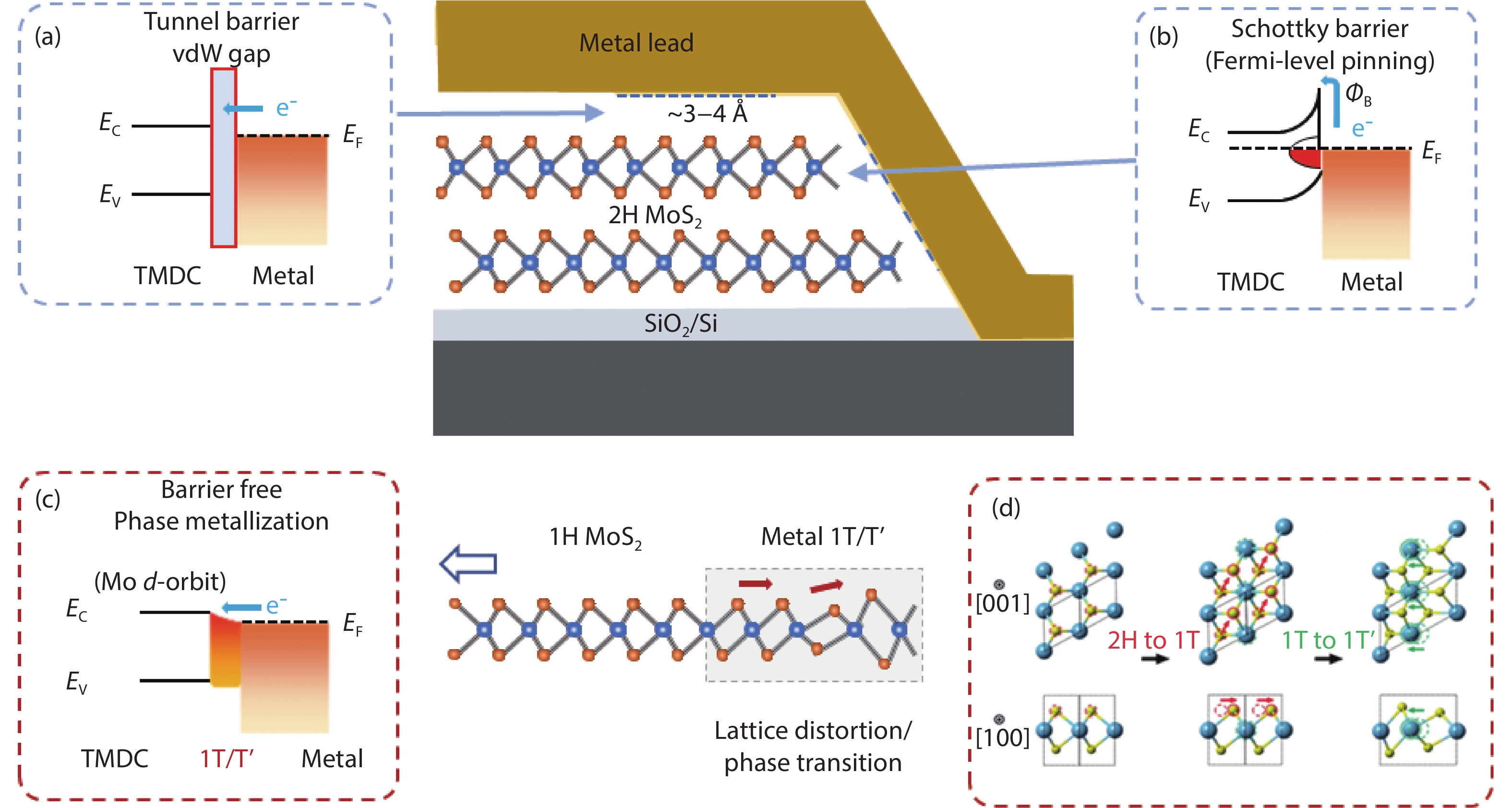
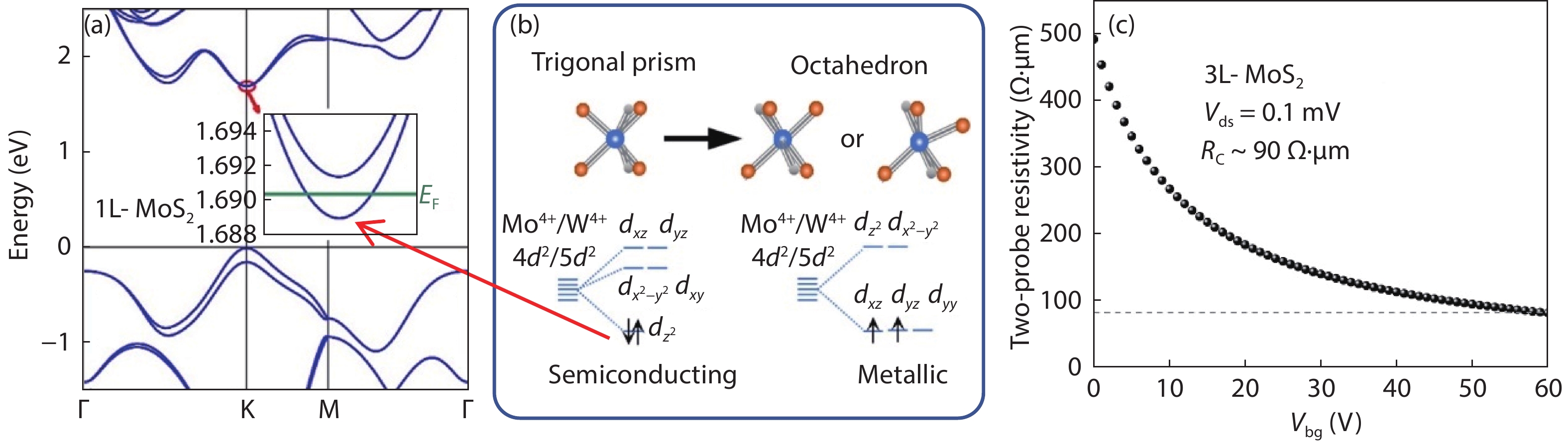
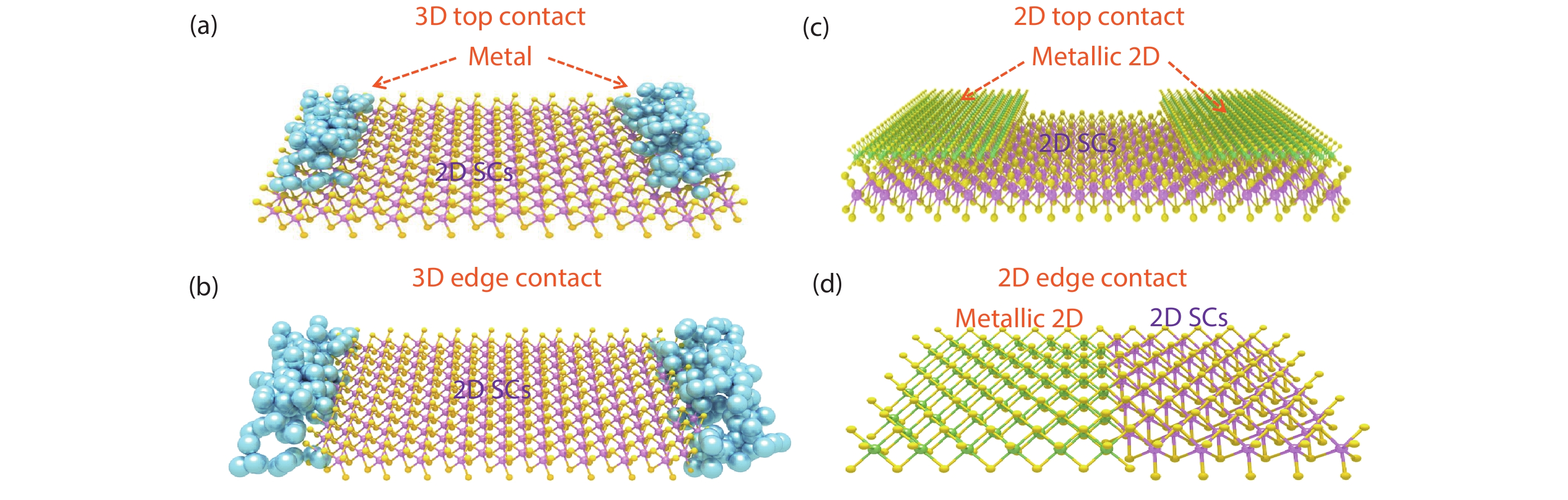
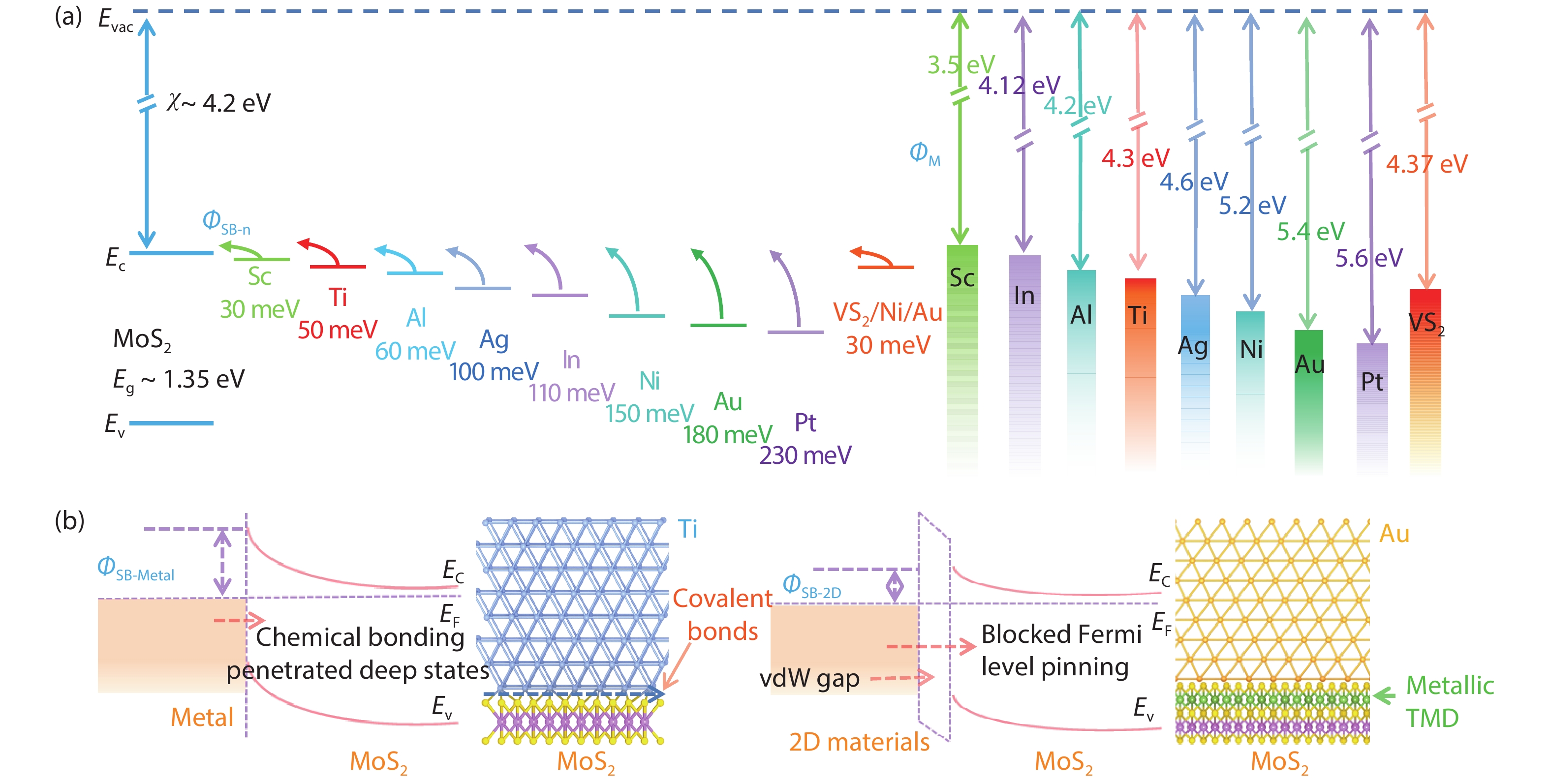
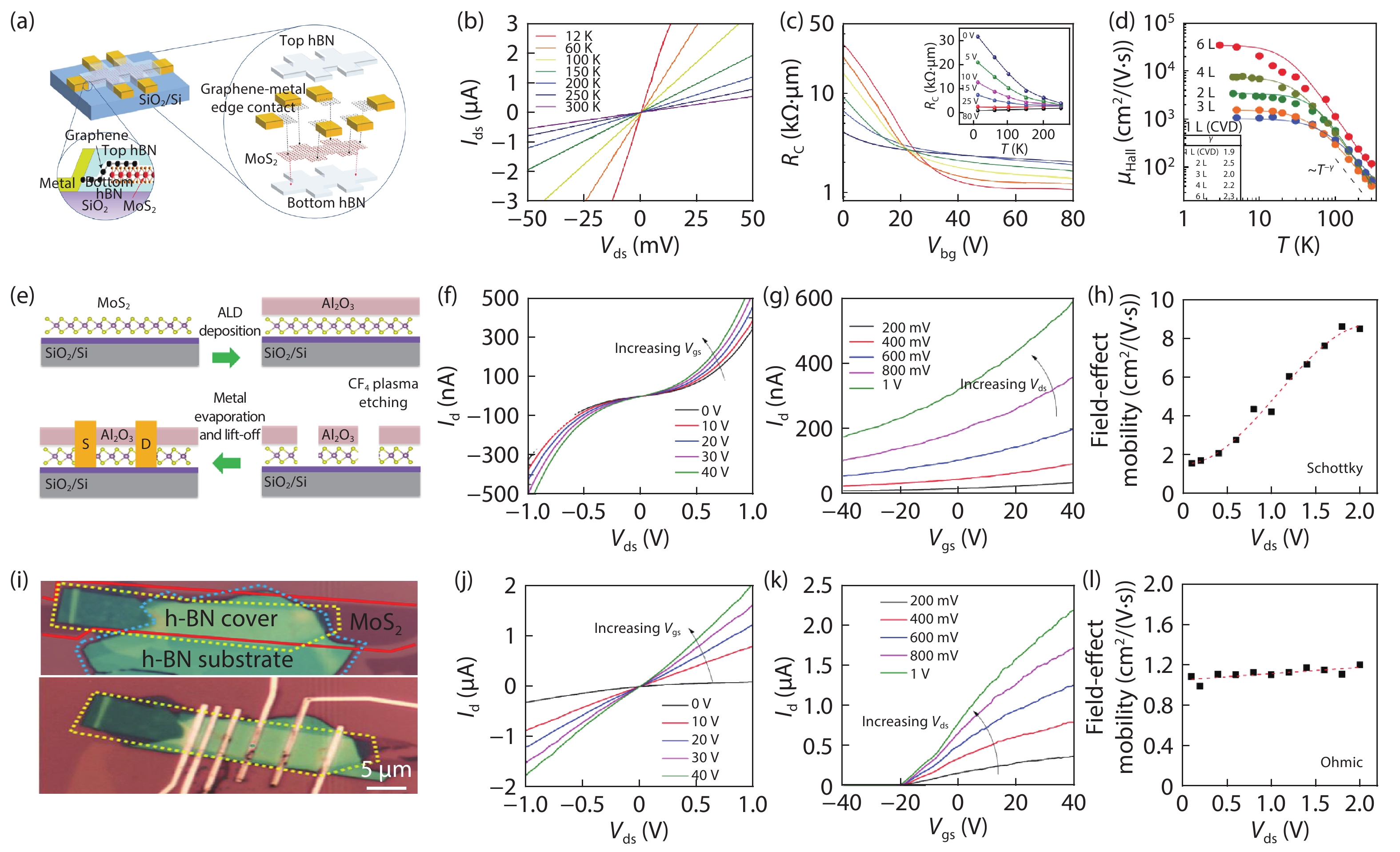
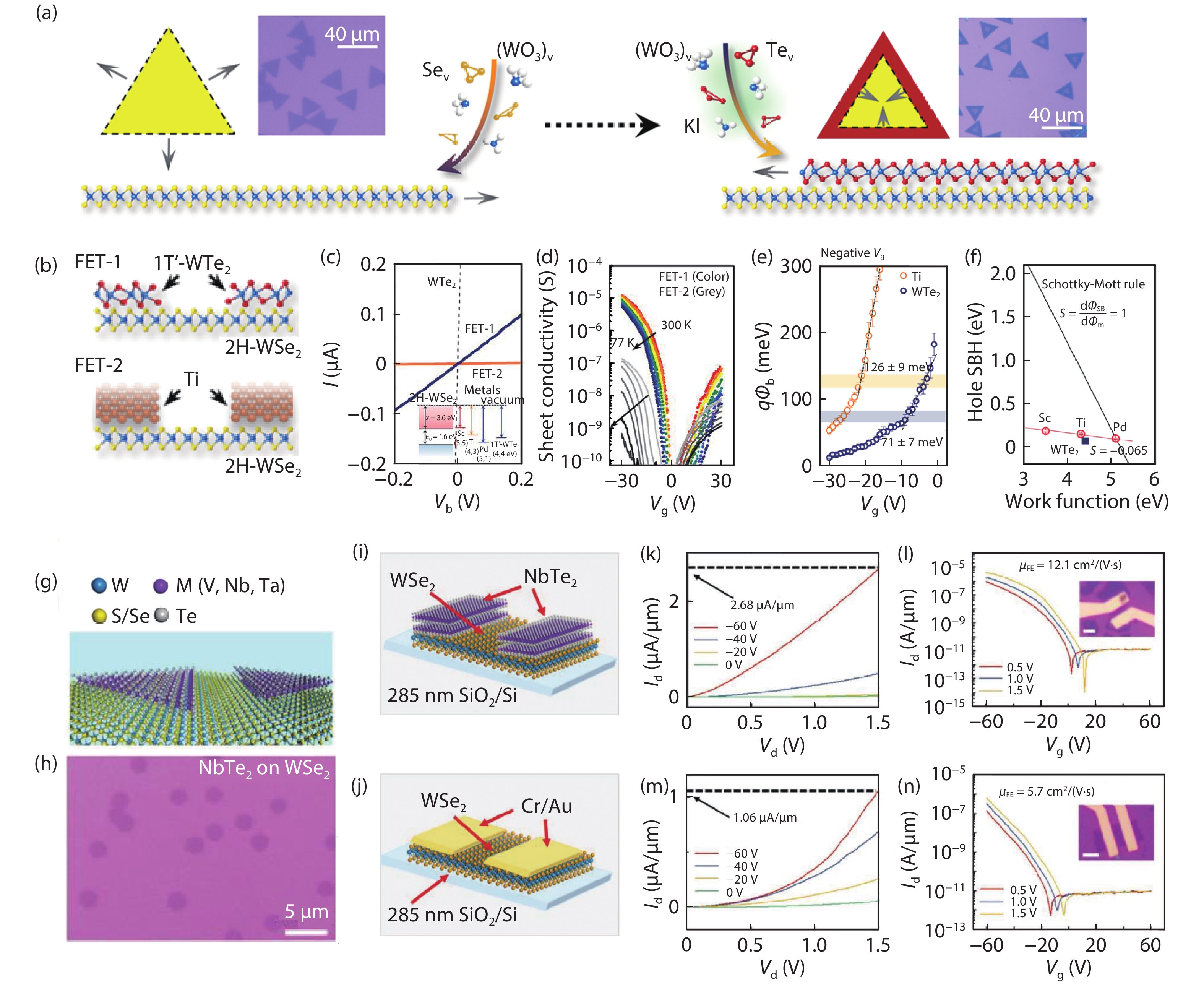
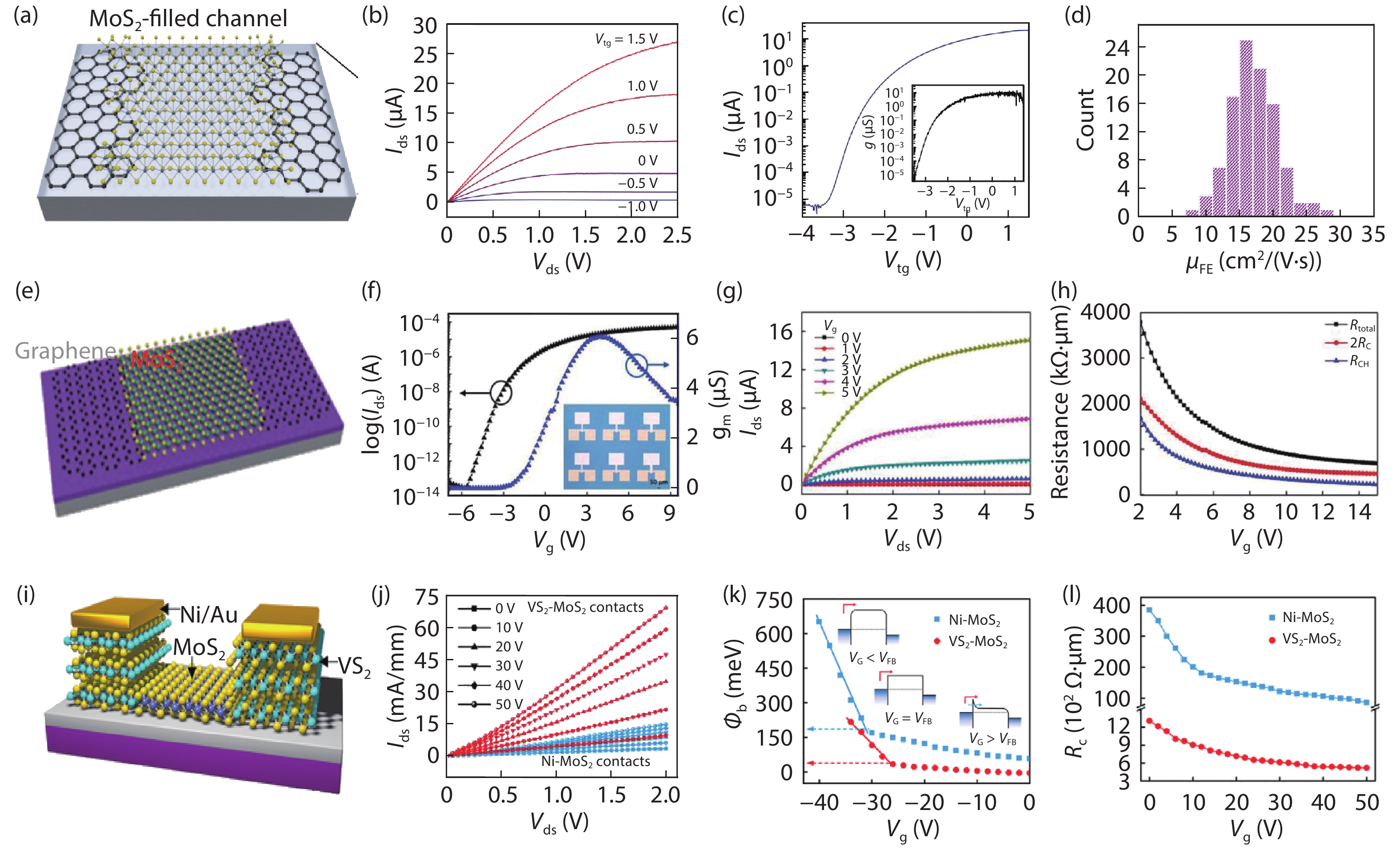
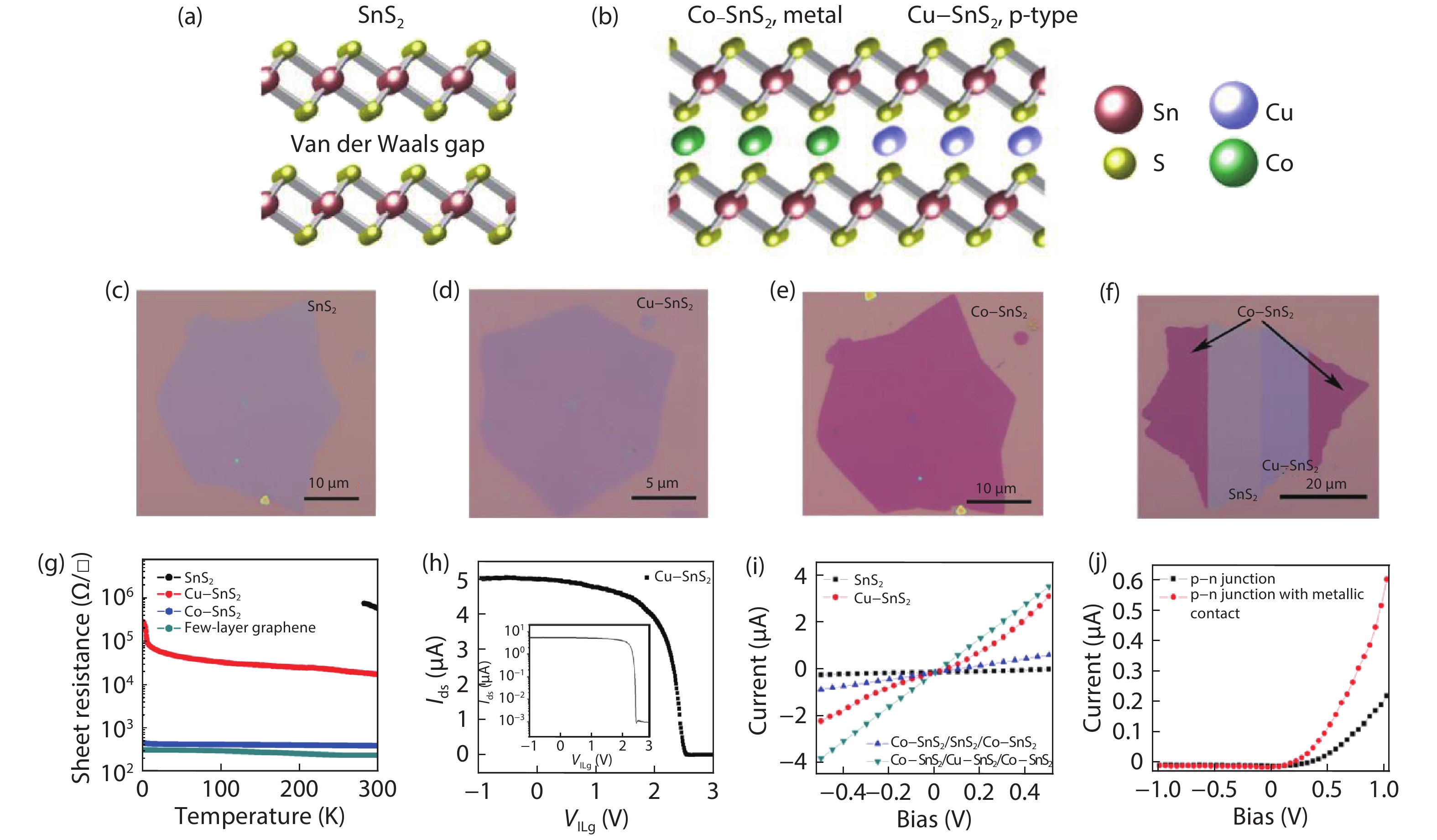
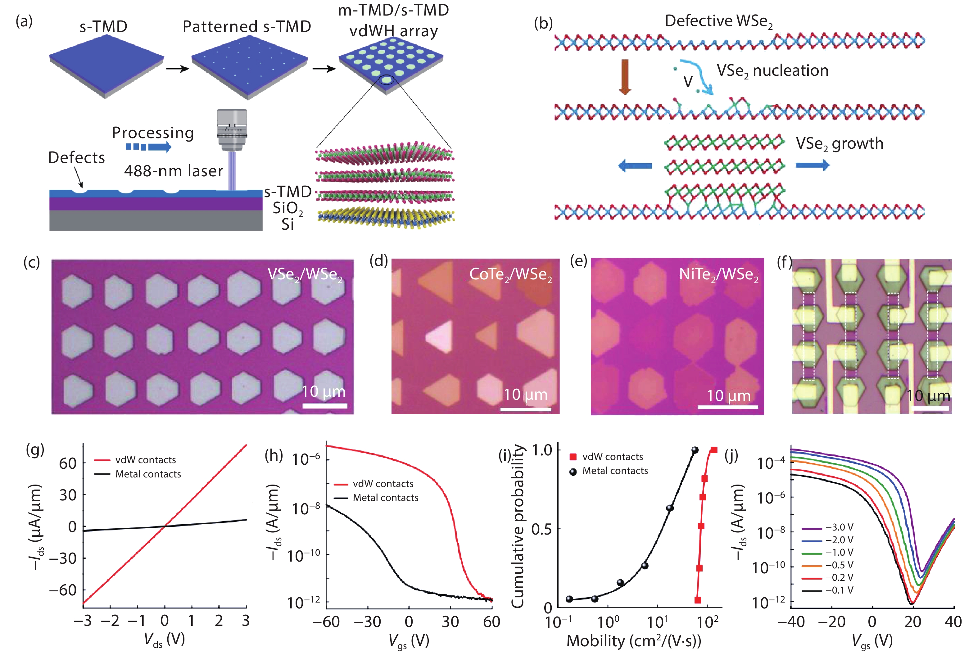
Two-dimensional (2D) layered materials, including graphene, black phosphorus (BP) and transition metal dichalcogenide (TMD) such as molybdenum disulfide (MoS2), tungsten diselenide (WSe2), have attracted increasing attention for the application in electronic and optoelectronic devices. Contacts, which are the communication links between these 2D materials and external circuitry, have significant effects on the performance of electronic and optoelectronic devices. However, the performance of devices based on 2D semiconductors (SCs) is often limited by the contacts. Here, we provide a comprehensive overview of the basic physics and role of contacts in 2D SCs, elucidating Schottky barrier nature and Fermi level pinning effect at metal/2D SCs contact interface. The progress of contact engineering, including traditional metals contacts and metallic 2D materials contacts, for improving the performance of 2D SCs based devices is presented. Traditional metal contacts, named 3D top and edge contacts, are discussed briefly. Meanwhile, methods of building 2D materials contacts (2D top contact and 2D edge contact) are discussed in detail, such as chemical vapor deposition (CVD) growth of 2D metallic material contacts, phase engineered metallic phase contacts and intercalation induced metallic state contacts. Finally, the challenges and opportunities of contact engineering for 2D SCs are outlined.


J. Semicond.
2020, 41(7): 072901 doi: 10.1088/1674-4926/41/7/072901
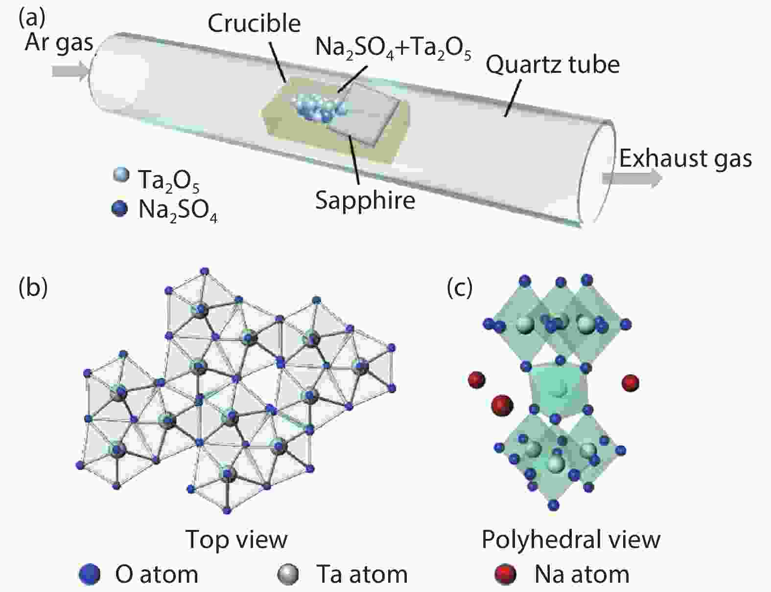
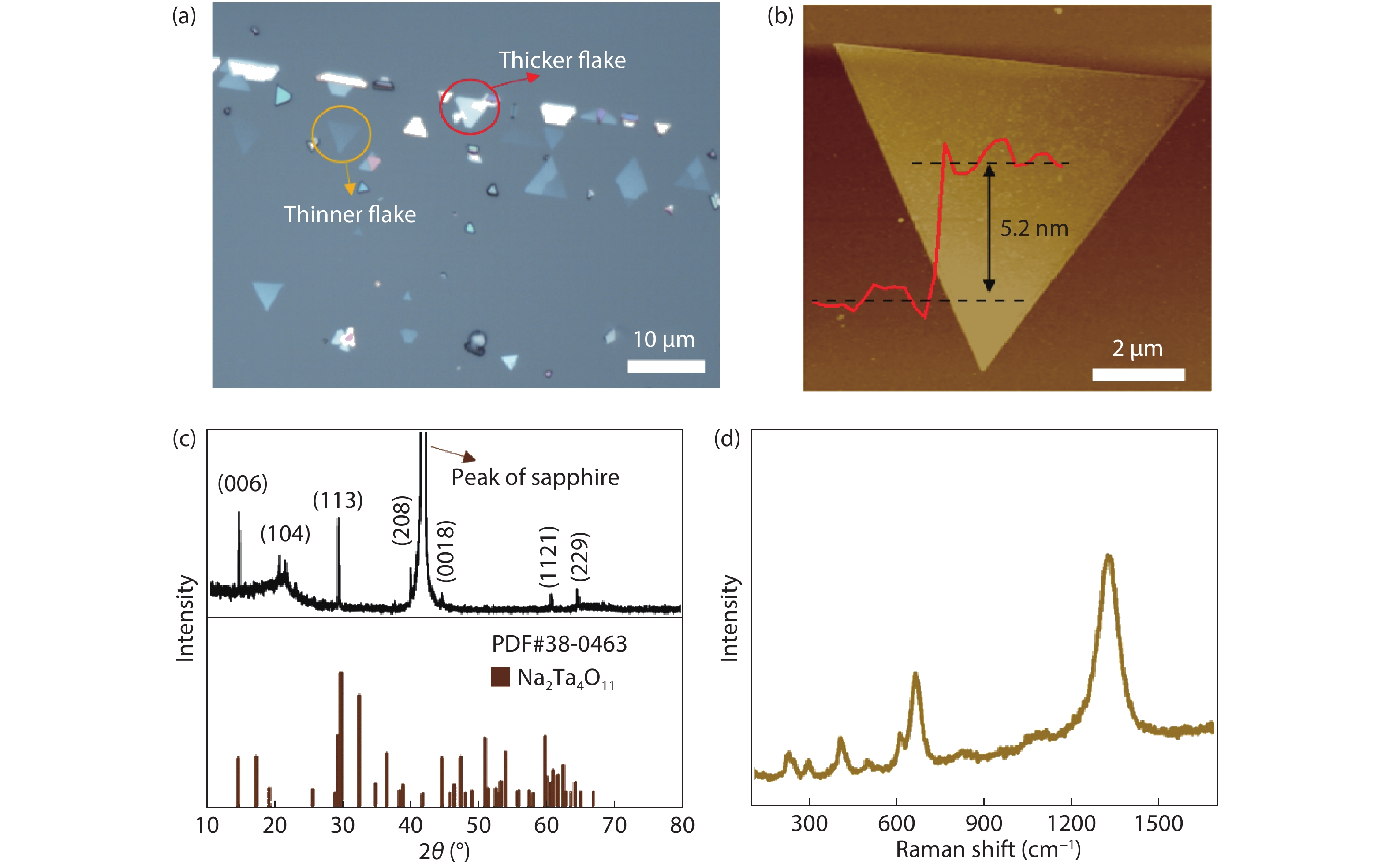
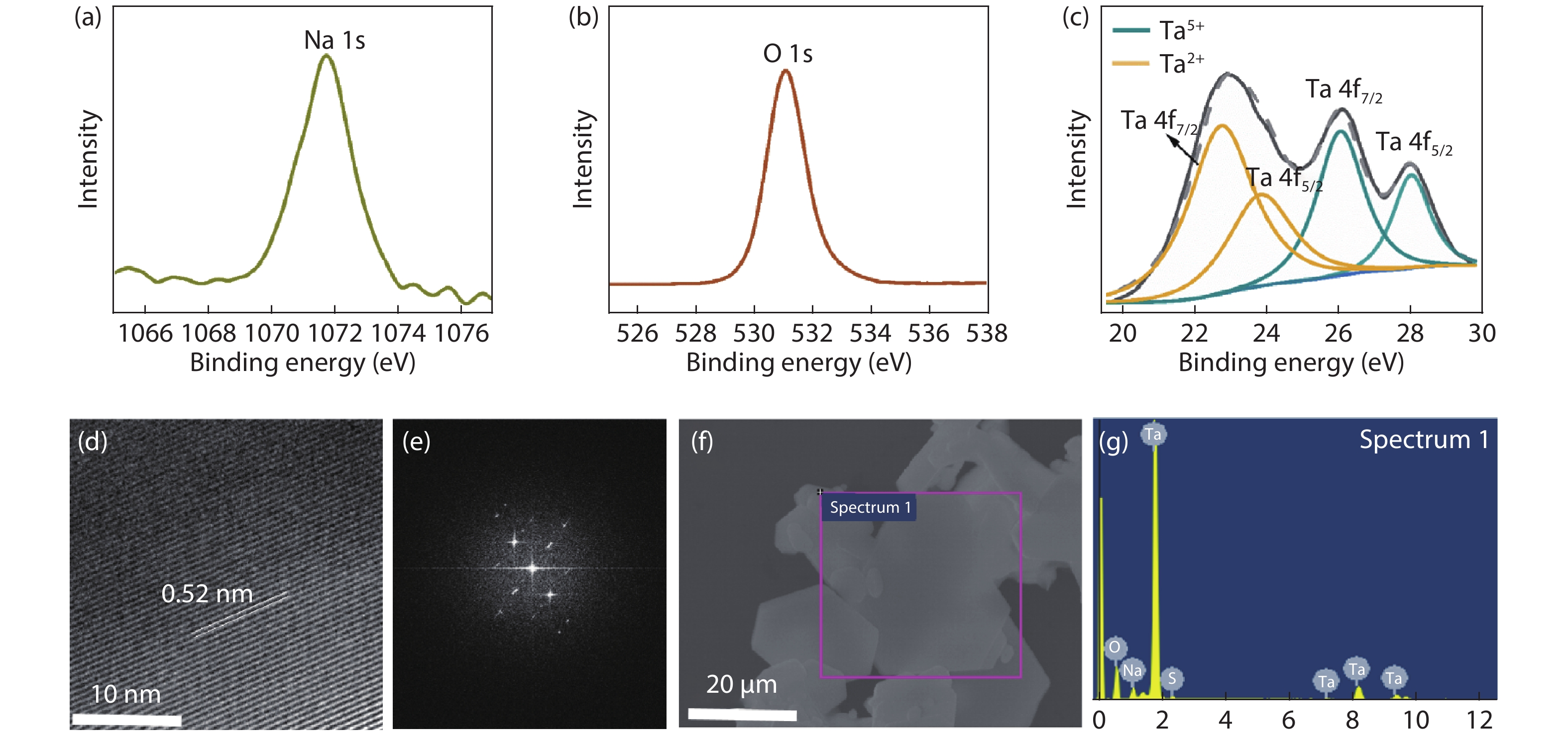
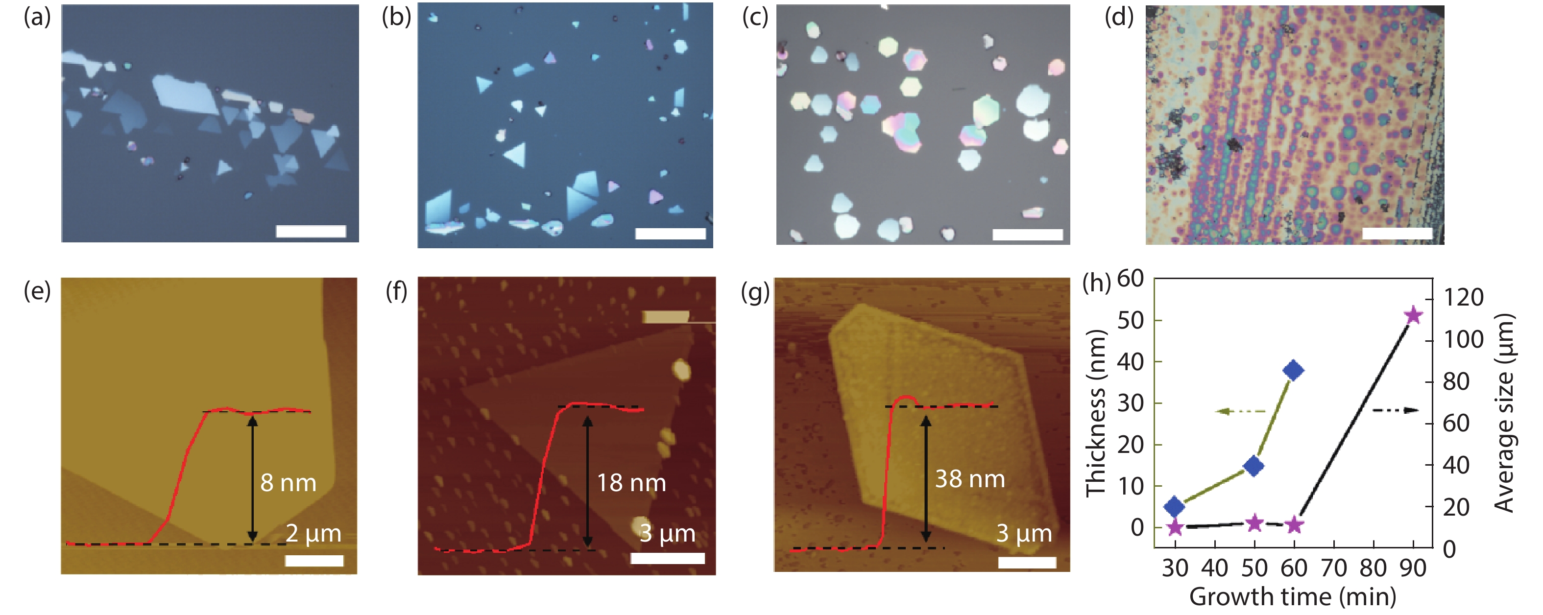
The insulator Na2Ta4O11 has been considered as a potential photocatalyst. However, little attention has been given to the synthesis of Na2Ta4O11 nanoparticles, let alone the growth of two-dimensional (2D) layered Na2Ta4O11 flake, which may bring innovative properties and promising applications. Here, the 2D thin-layer Na2Ta4O11 flake was first produced by chemical vapor deposition (CVD) method, with the smallest thickness reported currently. We have also synthesized 2D Na2Ta4O11 flake over 100 μm, which was the largest value over the 2D level reported to date. Our work proposed novel strategies to synthesize other 2D metal oxide material and endow the Na2Ta4O11 more properties and applications.
J. Semicond.
2020, 41(7): 072902 doi: 10.1088/1674-4926/41/7/072902
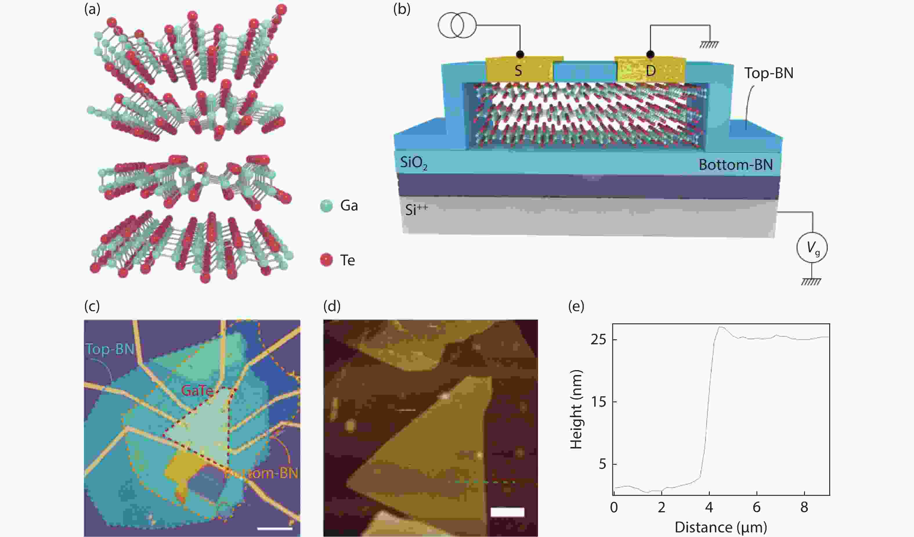
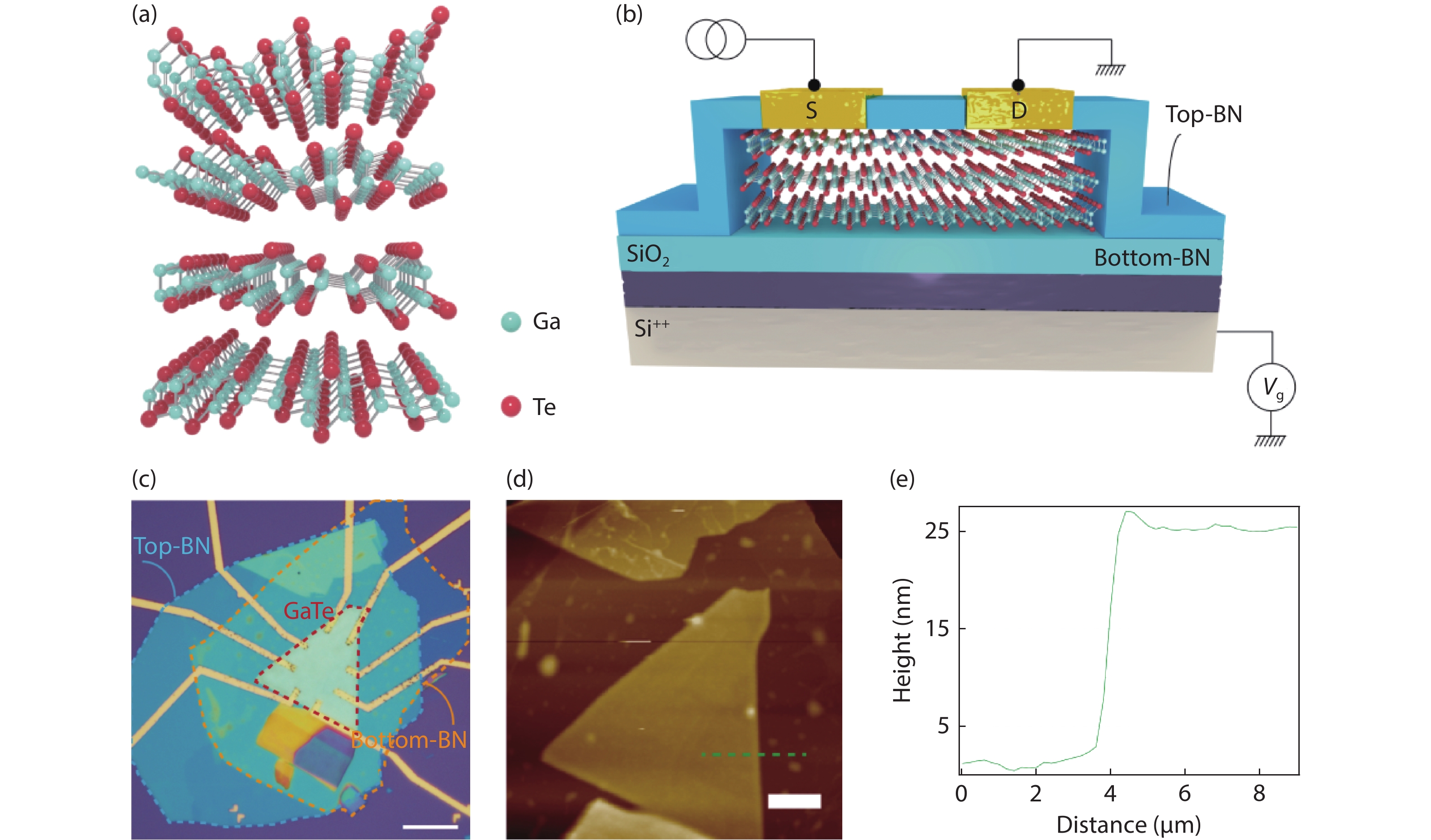
Two-dimensional (2D) materials have triggered enormous interest thanks to their interesting properties and potential applications, ranging from nanoelectronics to energy catalysis and biomedicals. In addition to other widely investigated 2D materials, GaTe, a layered material with a direct band gap of ~1.7 eV, is of importance for applications such as optoelectronics. However, detailed information on the transport properties of GaTe is yet to be explored, especially at low temperatures. Here, we report on electrical transport measurements on few-layered GaTe field effect transistors (FETs) encapsulated by h-BN at different temperatures. We find that by tuning the carrier density, ambipolar transport was realized in GaTe devices, and an electrical-field-induced metal to insulator transition (MIT) was observed when it was hole doped. The mobilities of GaTe devices show a clear dependence on temperature and increase with the decrease of temperature, reaching ~1200 cm2V−1s−1 at 3 K. Our findings may inspire further electronic studies in devices based on GaTe.

J. Semicond.
2020, 41(7): 072903 doi: 10.1088/1674-4926/41/7/072903
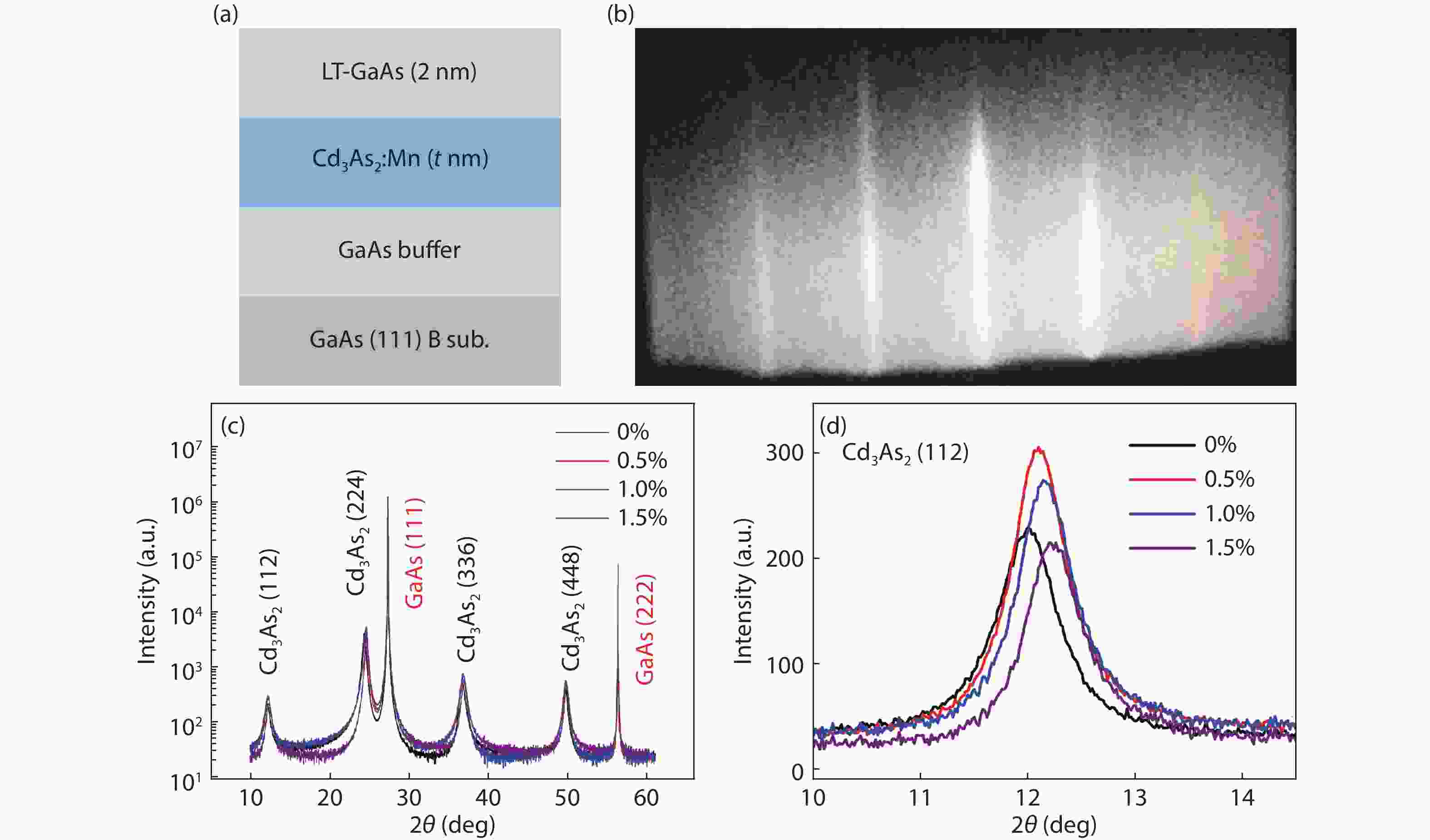
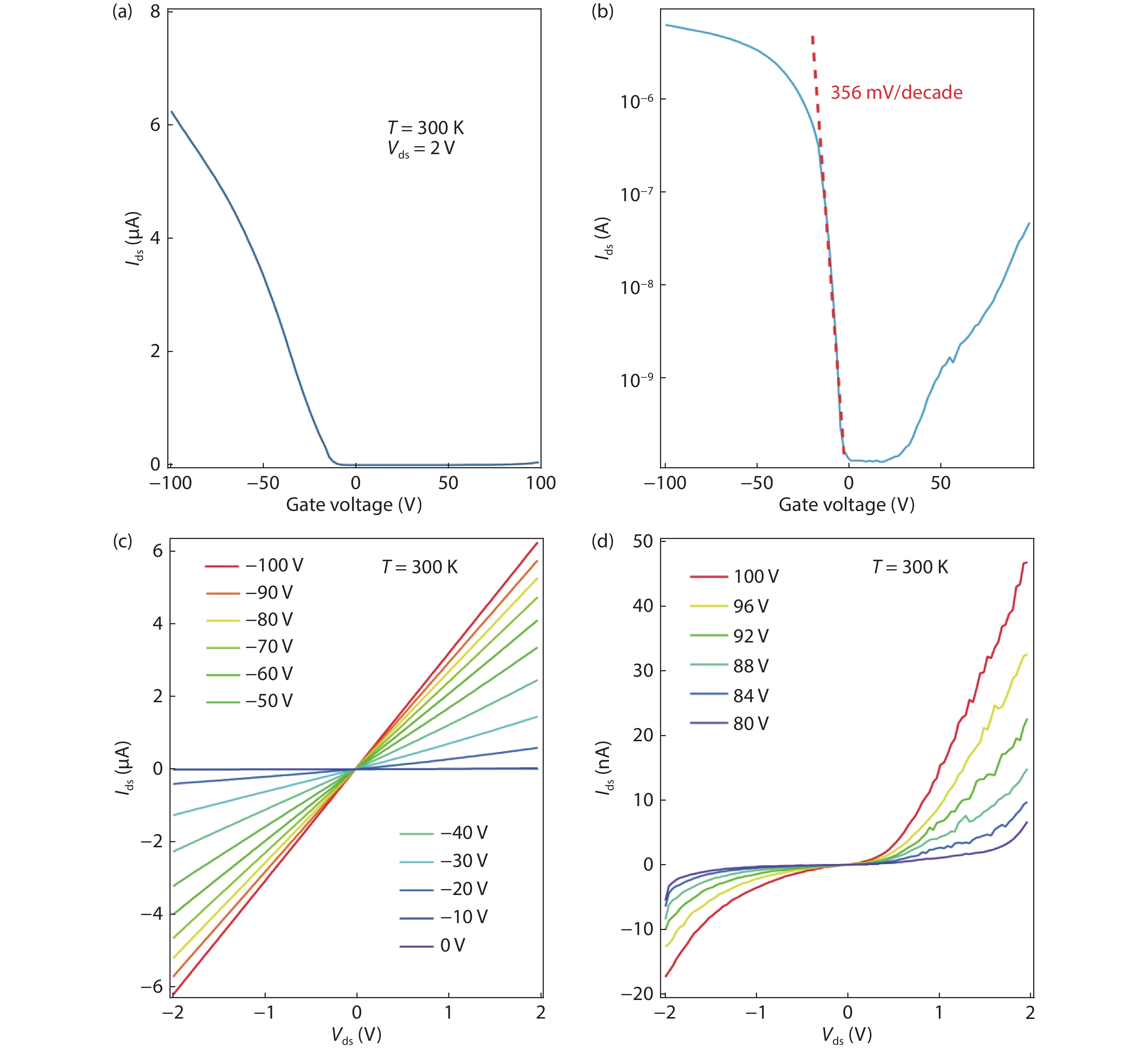
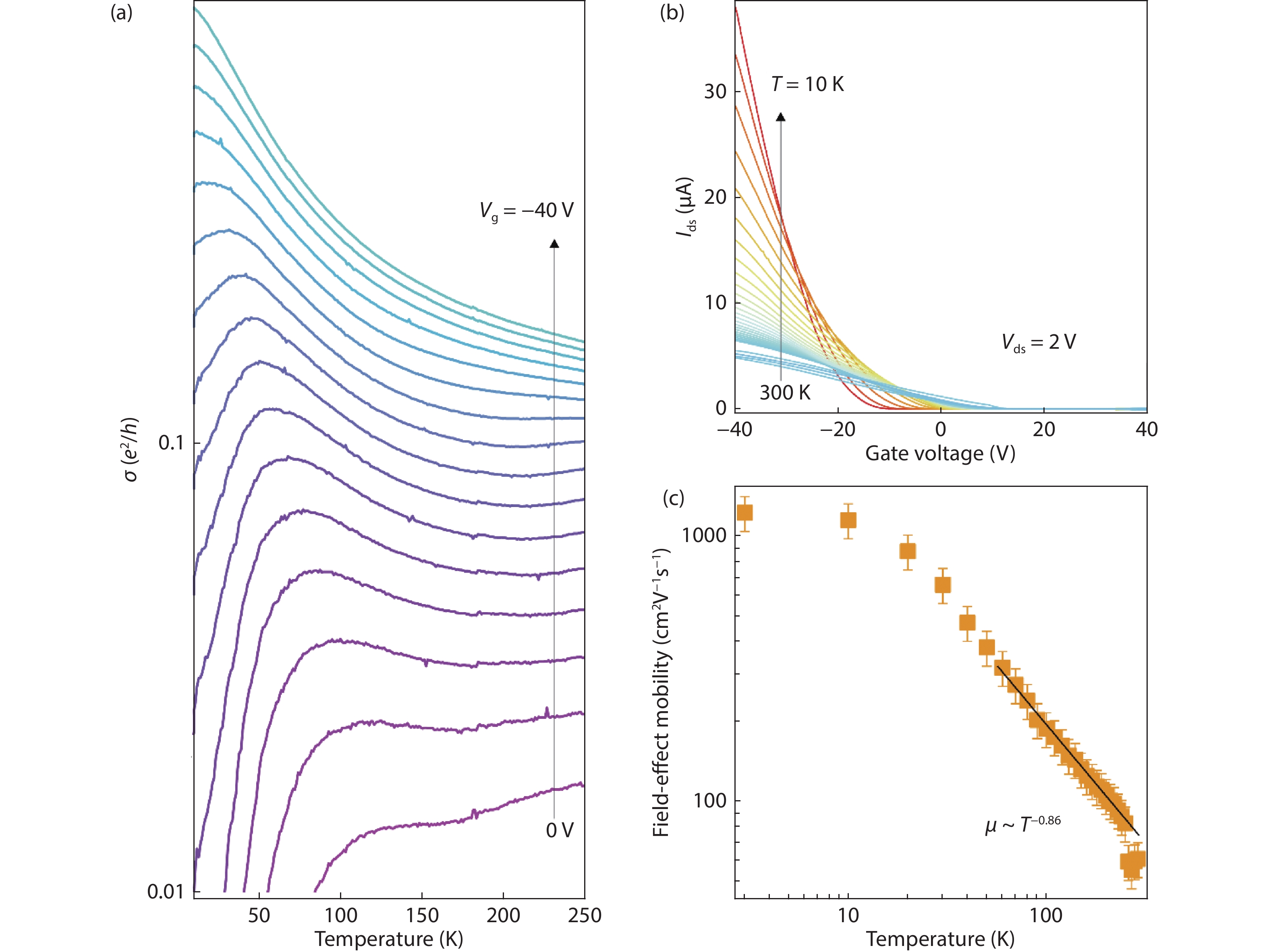
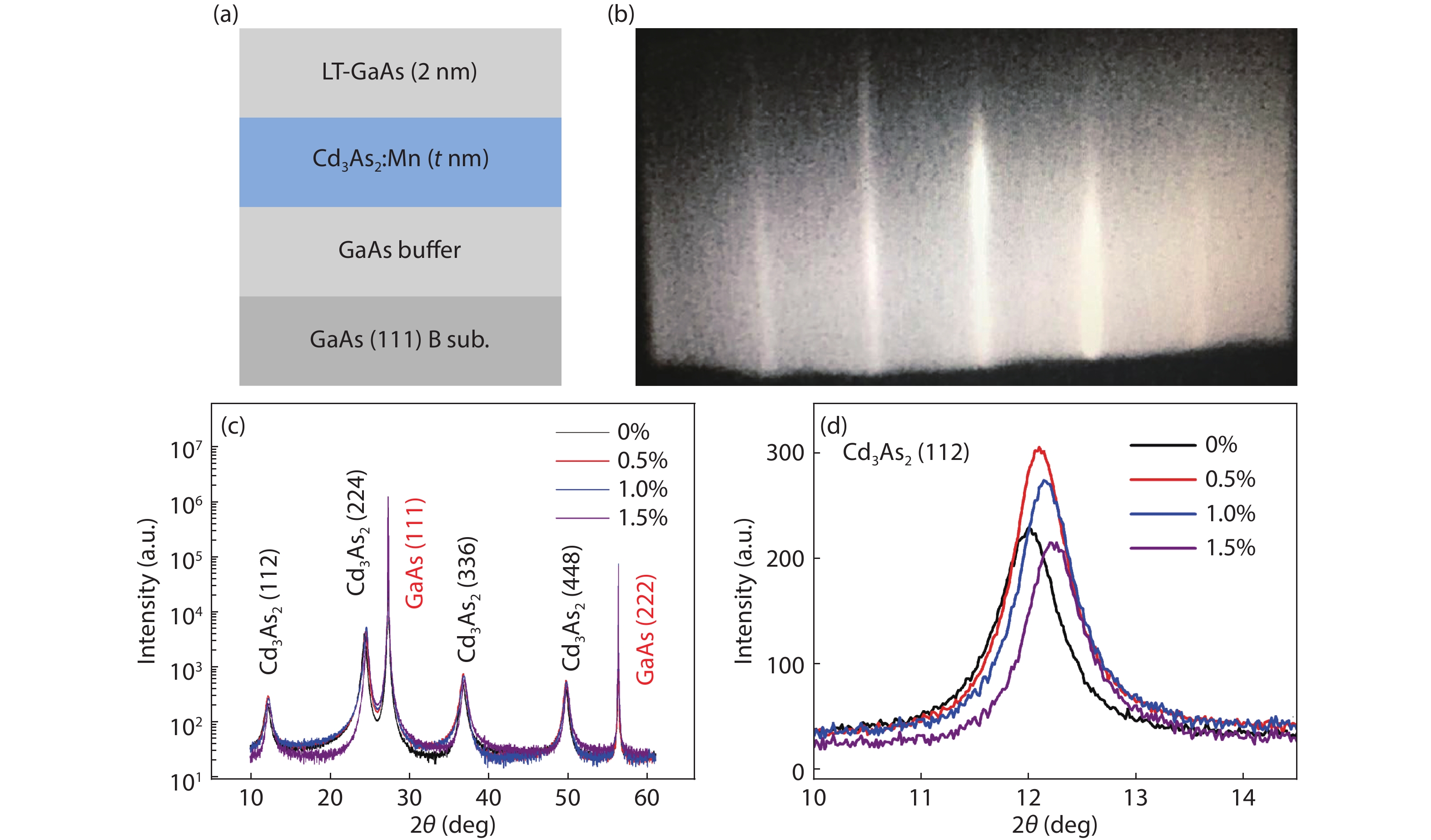
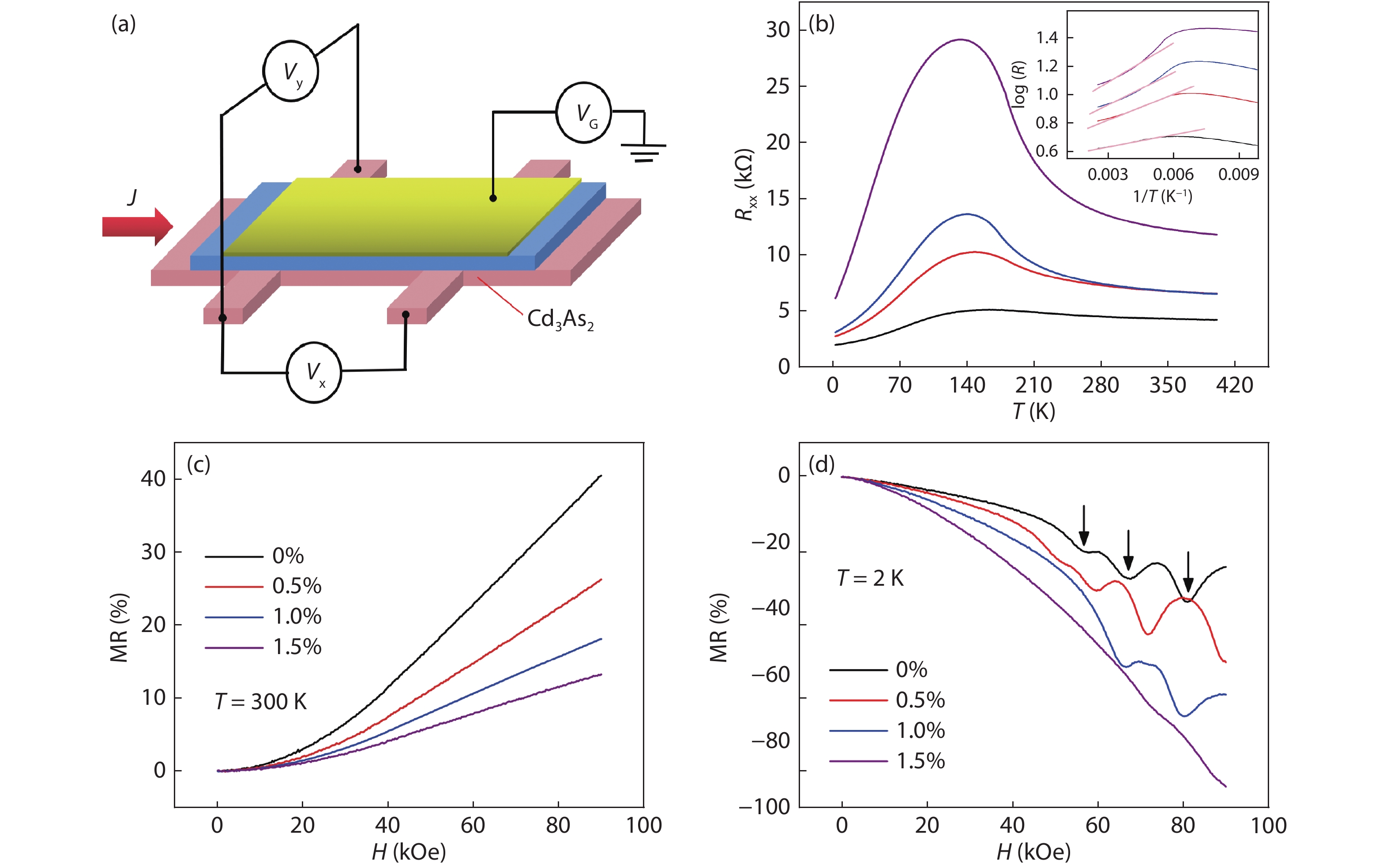
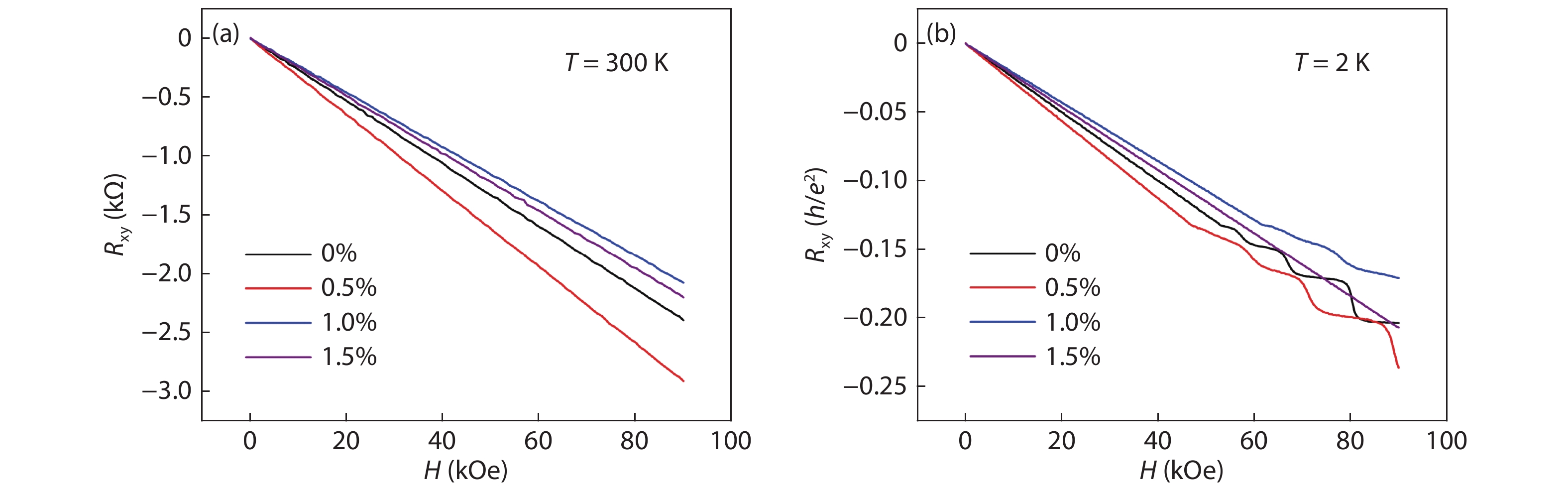
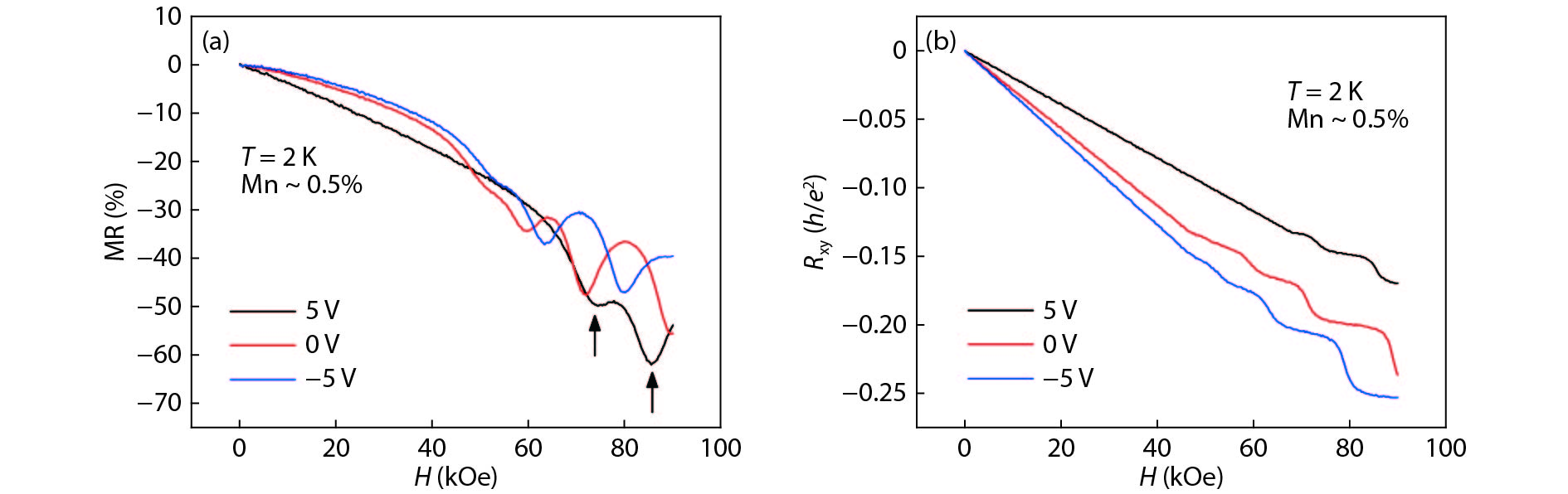
The Mn doping effects on the gate-tunable transport properties of topological Dirac semimetal Cd3As2 films have been investigated. Mn-doped Cd3As2 films are directly grown on GaAs(111)B substrates by molecular-beam epitaxy, during which the single crystal phase can be obtained with Mn concentration less than 2%. Shubnikov-de Haas oscillation and quantum Hall effect are observed at low temperatures, and electrons are found to be the dominant carrier in the whole temperature range. Higher Mn content results in smaller lattice constant, lower electron mobility and larger effective band gap, while the carrier density seems to be unaffected by Mn-doping. Gating experiments show that Shubnikov-de Haas oscillation and quantum Hall effect are slightly modulated by electric field, which can be explained by the variation of electron density. Our results provide useful information for understanding the magnetic element doping effects on the transport properties of Cd3As2 films.
J. Semicond.
2020, 41(7): 072904 doi: 10.1088/1674-4926/41/7/072904
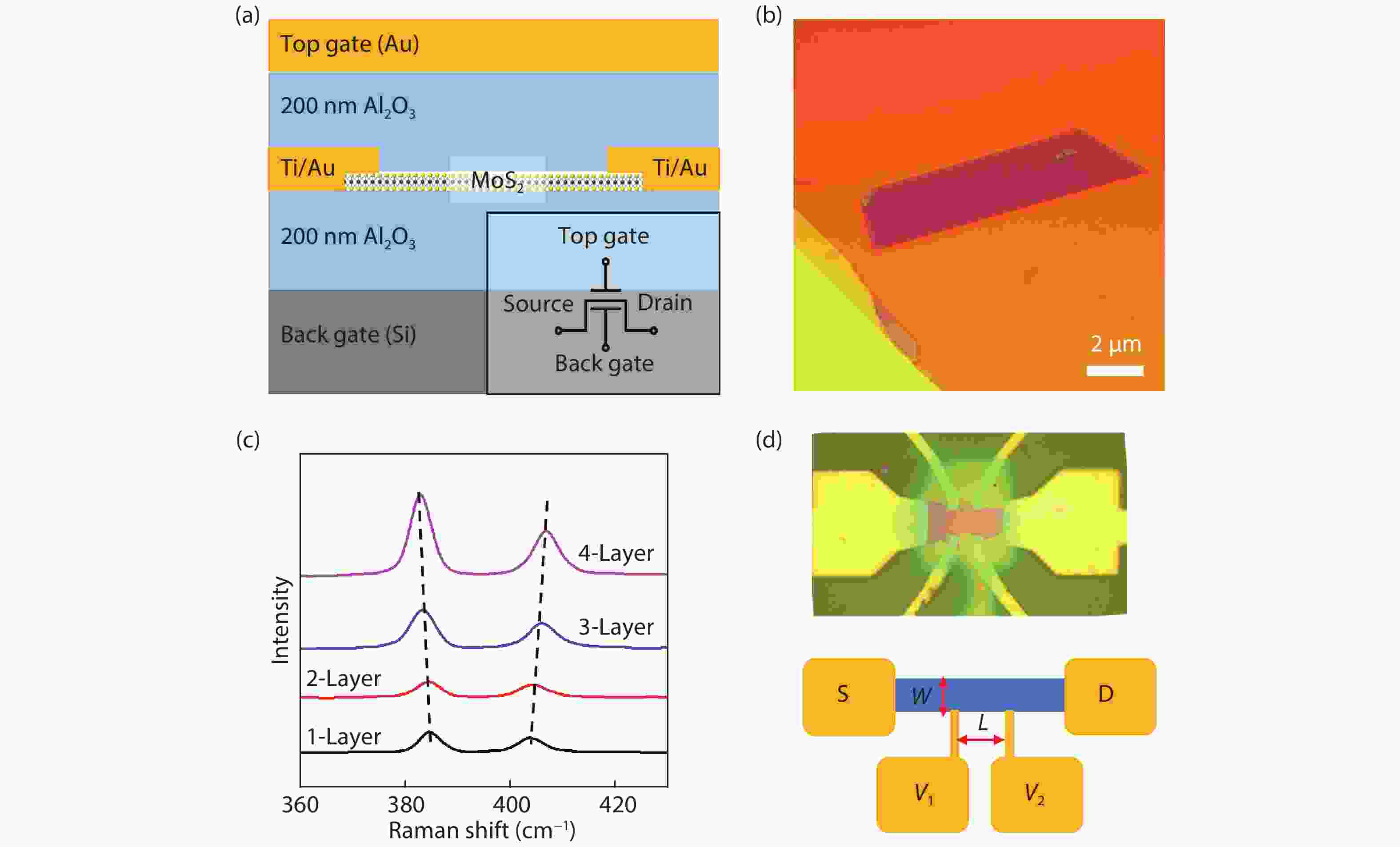
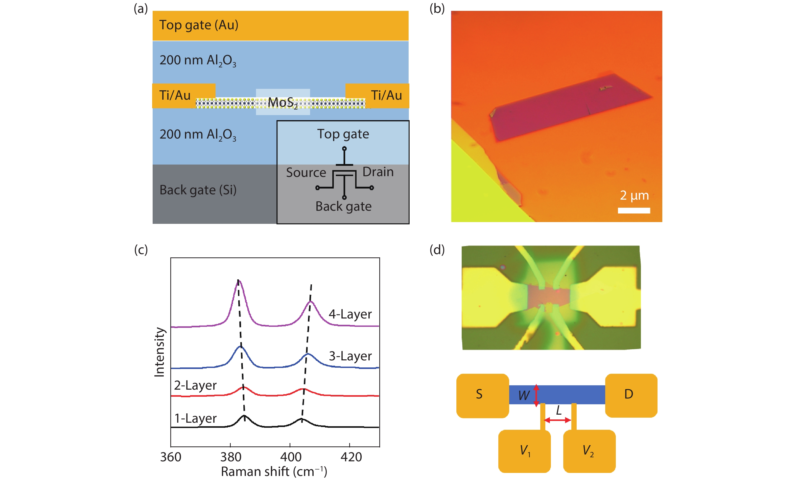
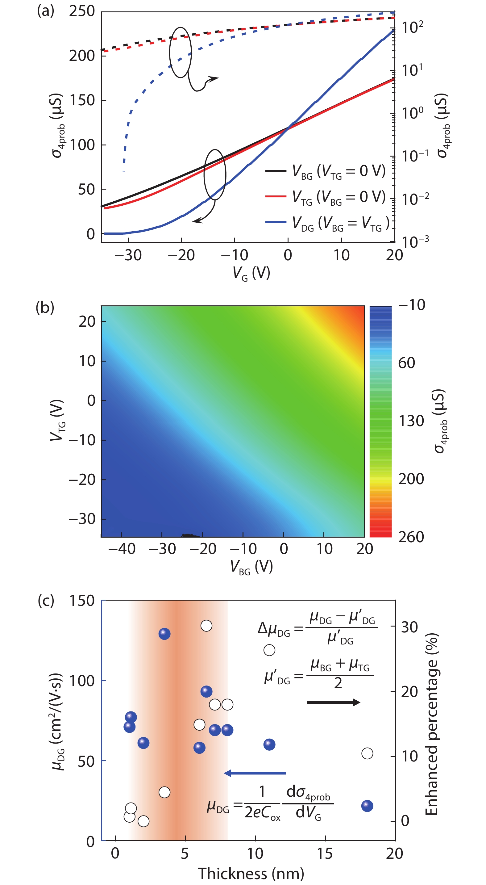
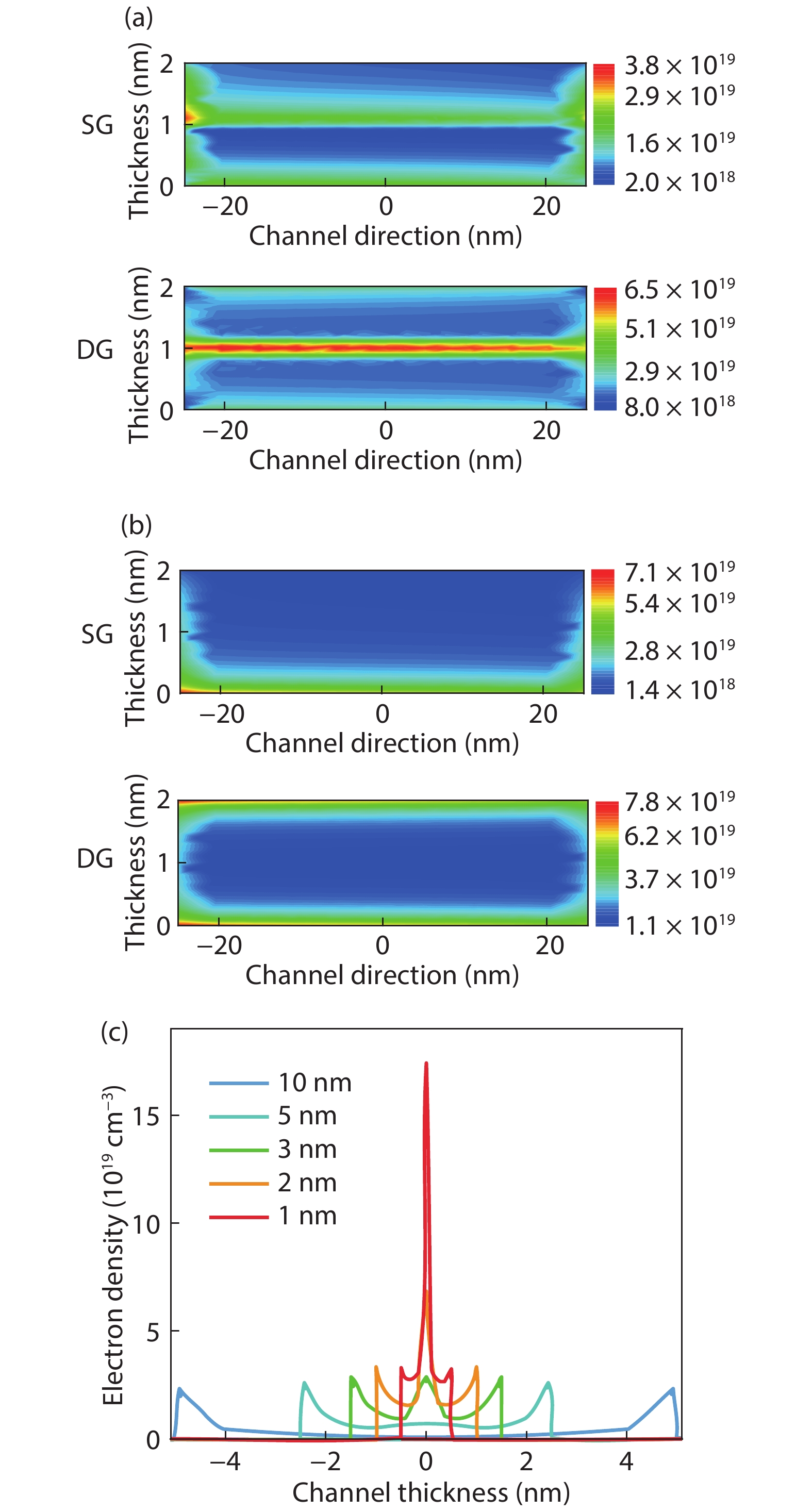
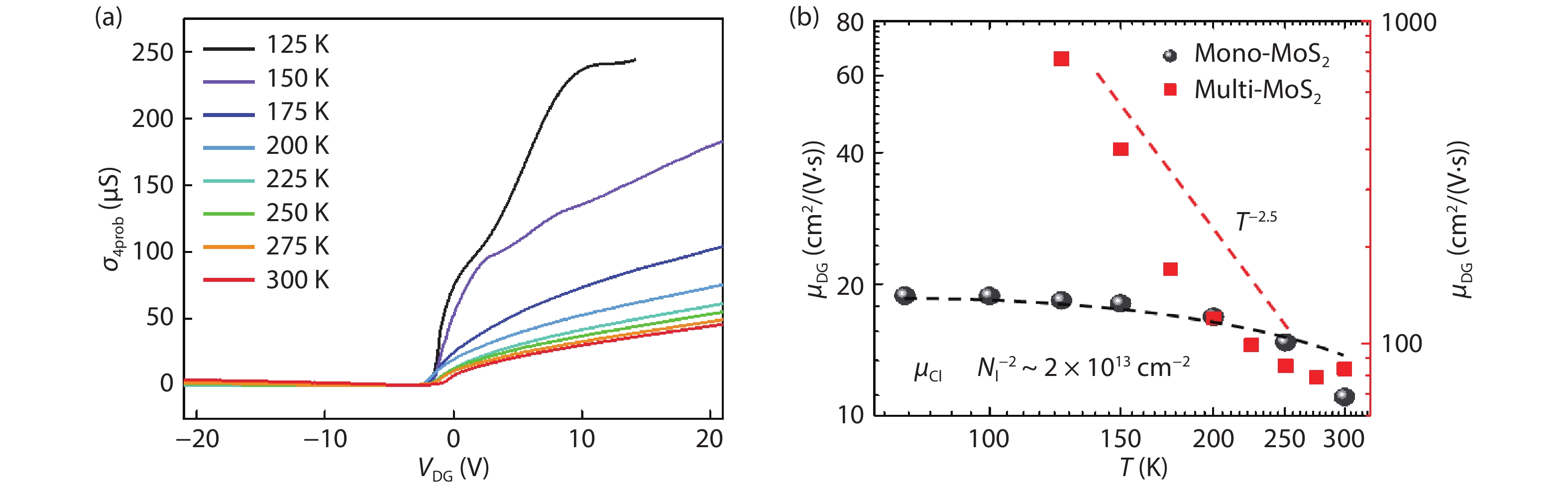
Semiconductive two dimensional (2D) materials have attracted significant research attention due to their rich band structures and promising potential for next-generation electrical devices. In this work, we investigate the MoS2 field-effect transistors (FETs) with a dual-gated (DG) architecture, which consists of symmetrical thickness for back gate (BG) and top gate (TG) dielectric. The thickness-dependent charge transport in our DG-MoS2 device is revealed by a four-terminal electrical measurement which excludes the contact influence, and the TCAD simulation is also applied to explain the experimental data. Our results indicate that the impact of quantum confinement effect plays an important role in the charge transport in the MoS2 channel, as it confines charge carriers in the center of the channel, which reduces the scattering and boosts the mobility compared to the single gating case. Furthermore, temperature-dependent transfer curves reveal that multi-layer MoS2 DG-FET is in the phonon-limited transport regime, while single layer MoS2 shows typical Coulomb impurity limited regime.
J. Semicond.
2020, 41(7): 072905 doi: 10.1088/1674-4926/41/7/072905

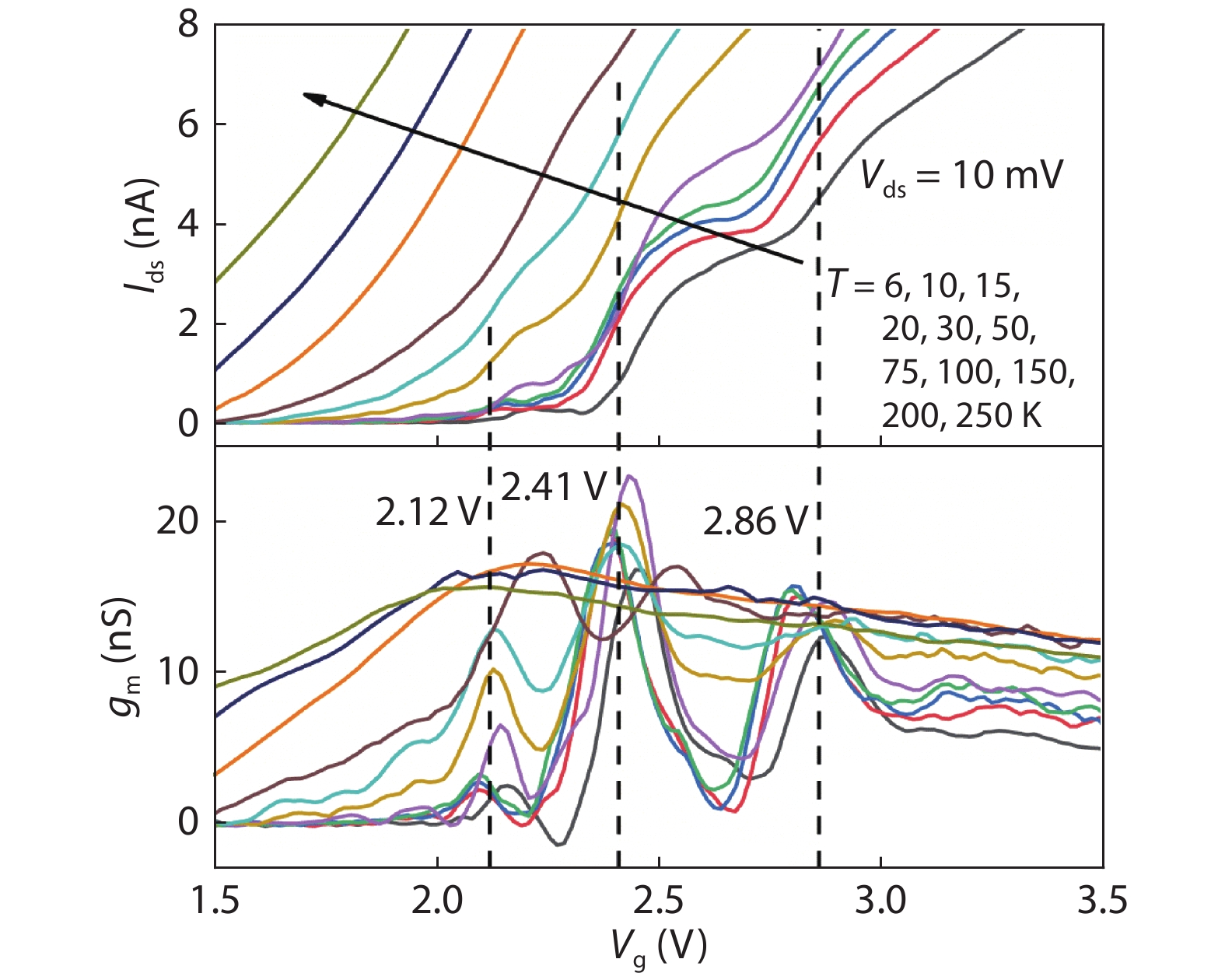
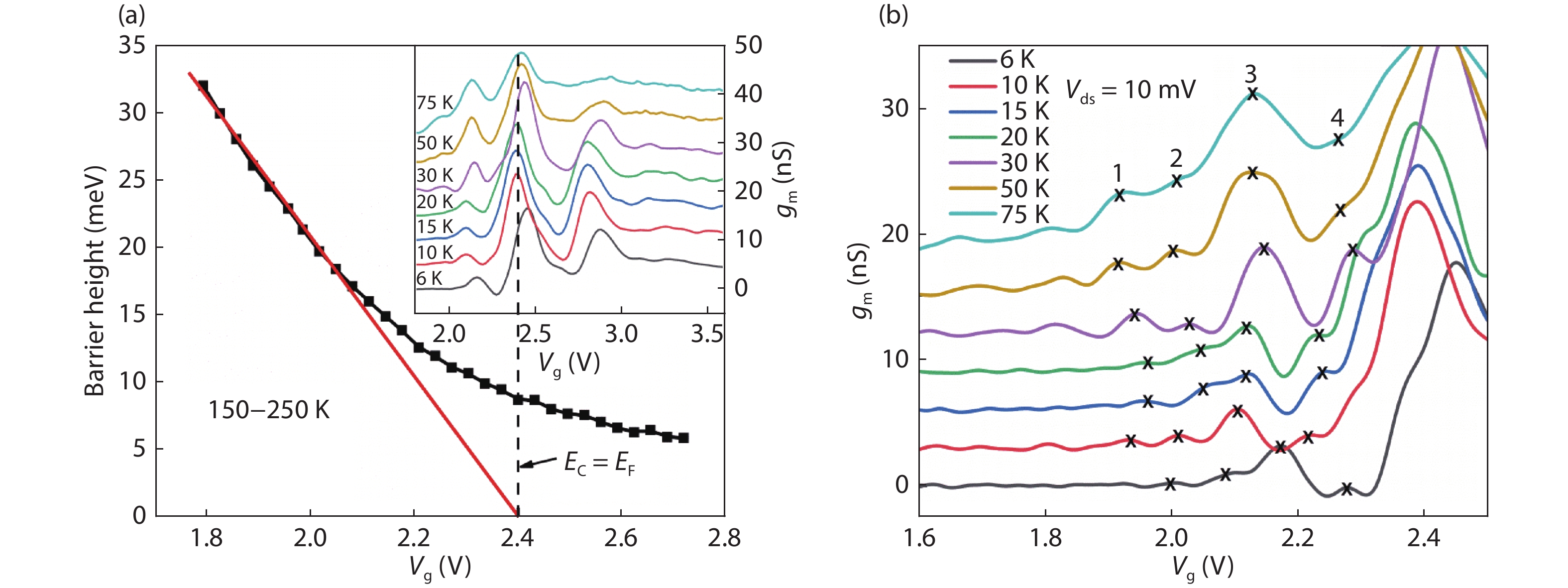
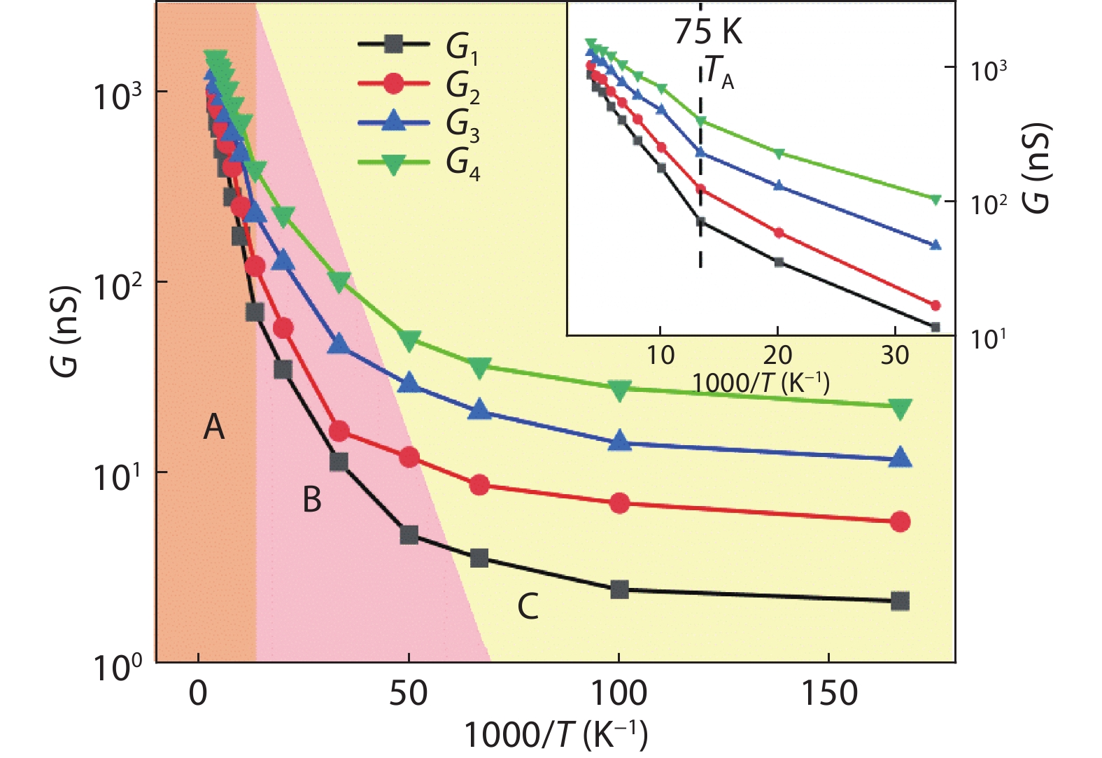
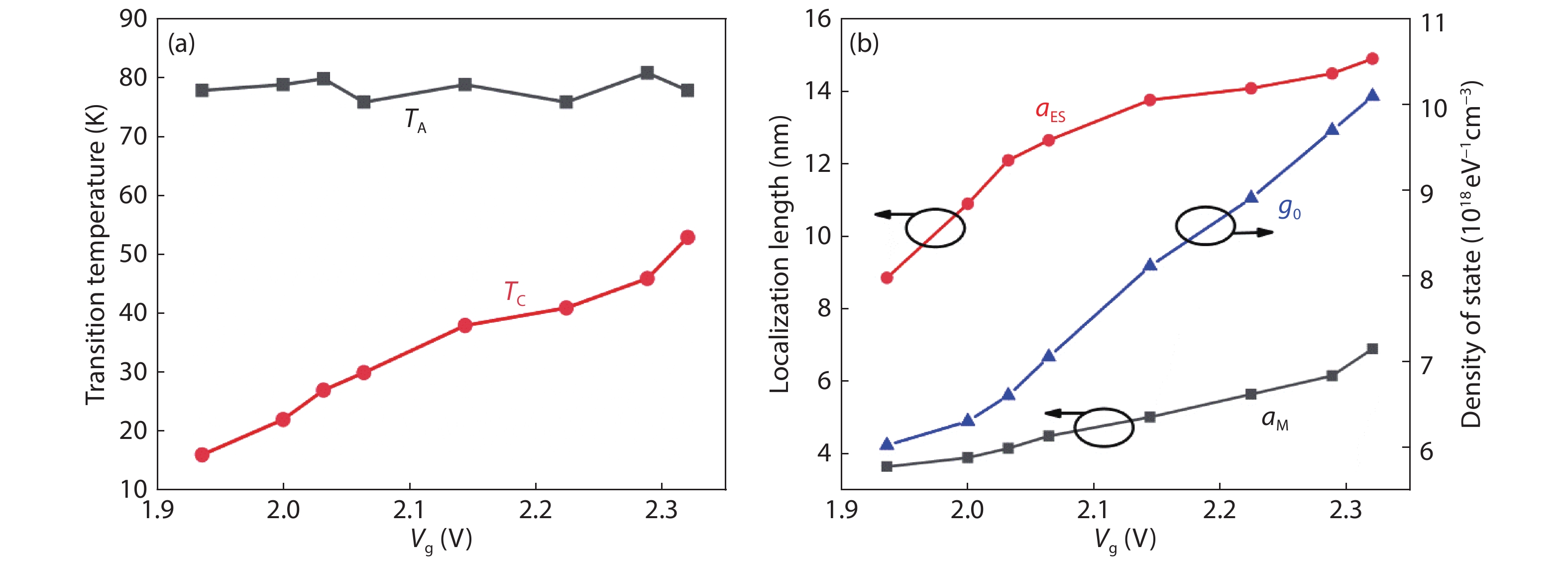
We investigate gate-regulated transition temperatures for electron hopping behaviours through discrete ionized dopant atoms in silicon junctionless nanowire transistors. We demonstrate that the localization length of the wave function in the spatial distribution is able to be manipulated by the gate electric field. The transition temperatures regulated as the function of the localization length and the density of states near the Fermi energy level allow us to understand the electron hopping behaviours under the influence of thermal activation energy and Coulomb interaction energy. This is useful for future quantum information processing by single dopant atoms in silicon.


J. Semicond.
2020, 41(7): 072906 doi: 10.1088/1674-4926/41/7/072906
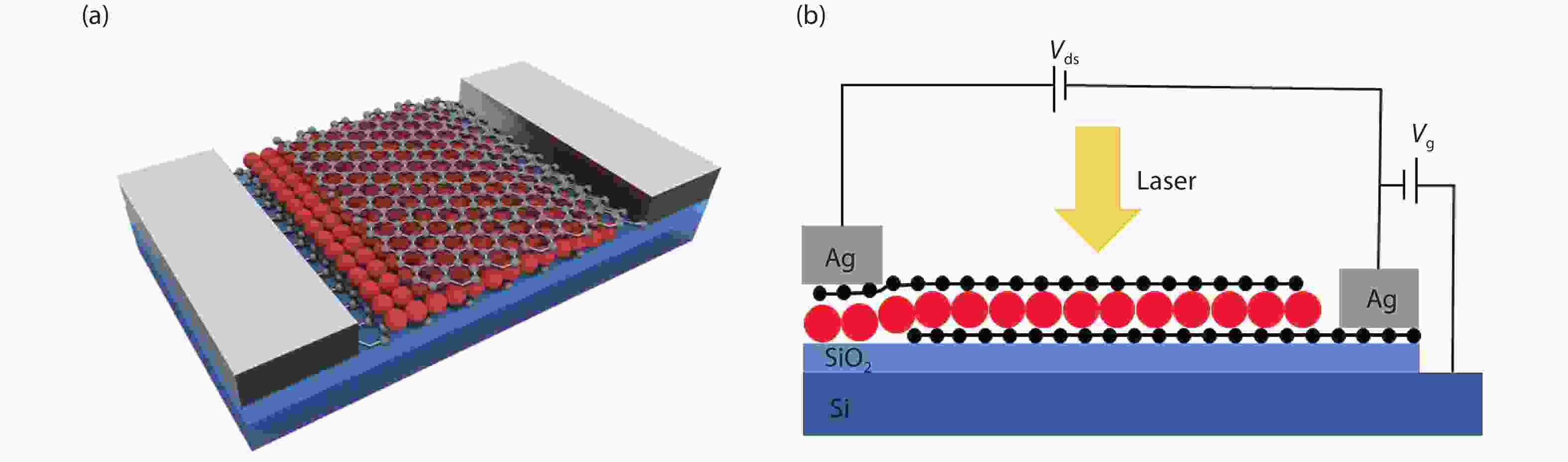
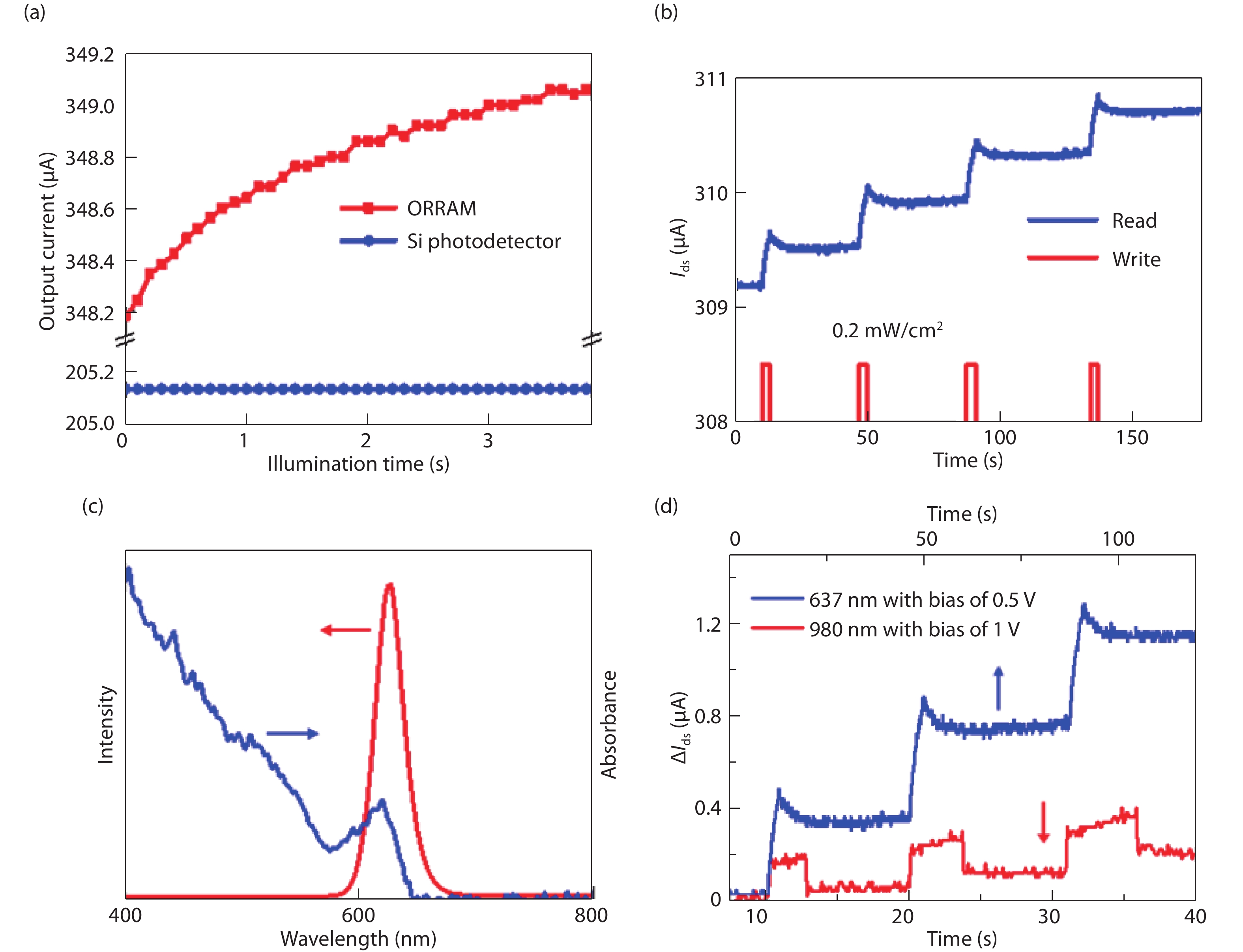
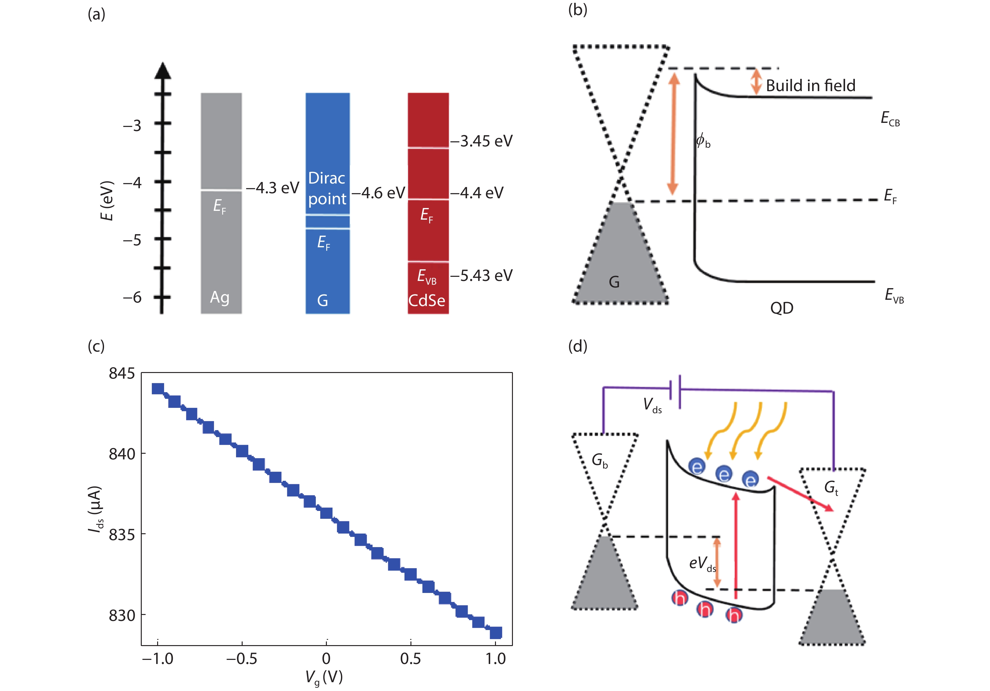
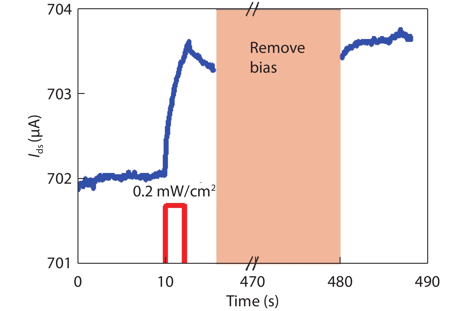
Emulating synaptic plasticity in an artificial neural network is crucial to mimic the basic functions of the human brain. In this work, we report a new optoelectronic resistive random access memory (ORRAM) in a three-layer vertical heterostructure of graphene/CdSe quantum dots (QDs)/graphene, which shows non-volatile multi-level optical memory under optical stimuli, giving rise to light-tunable synaptic behaviors. The optical non-volatile storage time is up to ~450 s. The device realizes the function of multi-level optical storage through the interlayer changes between graphene and QDs. This work highlights the feasibility for applying two-dimensional (2D) materials in ORRAM and optoelectronic synaptic devices towards artificial vision.


J. Semicond.
2020, 41(7): 072907 doi: 10.1088/1674-4926/41/7/072907
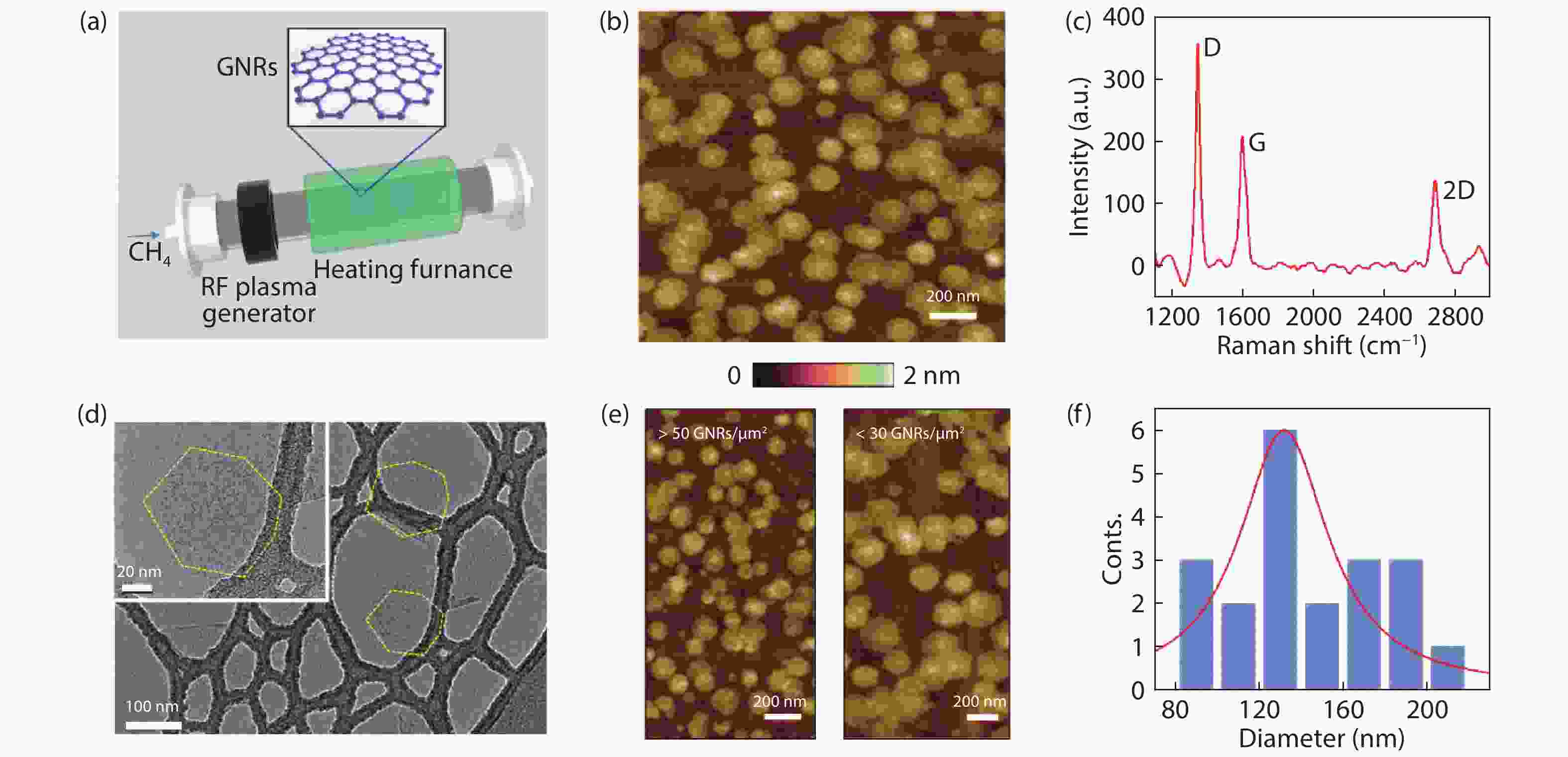
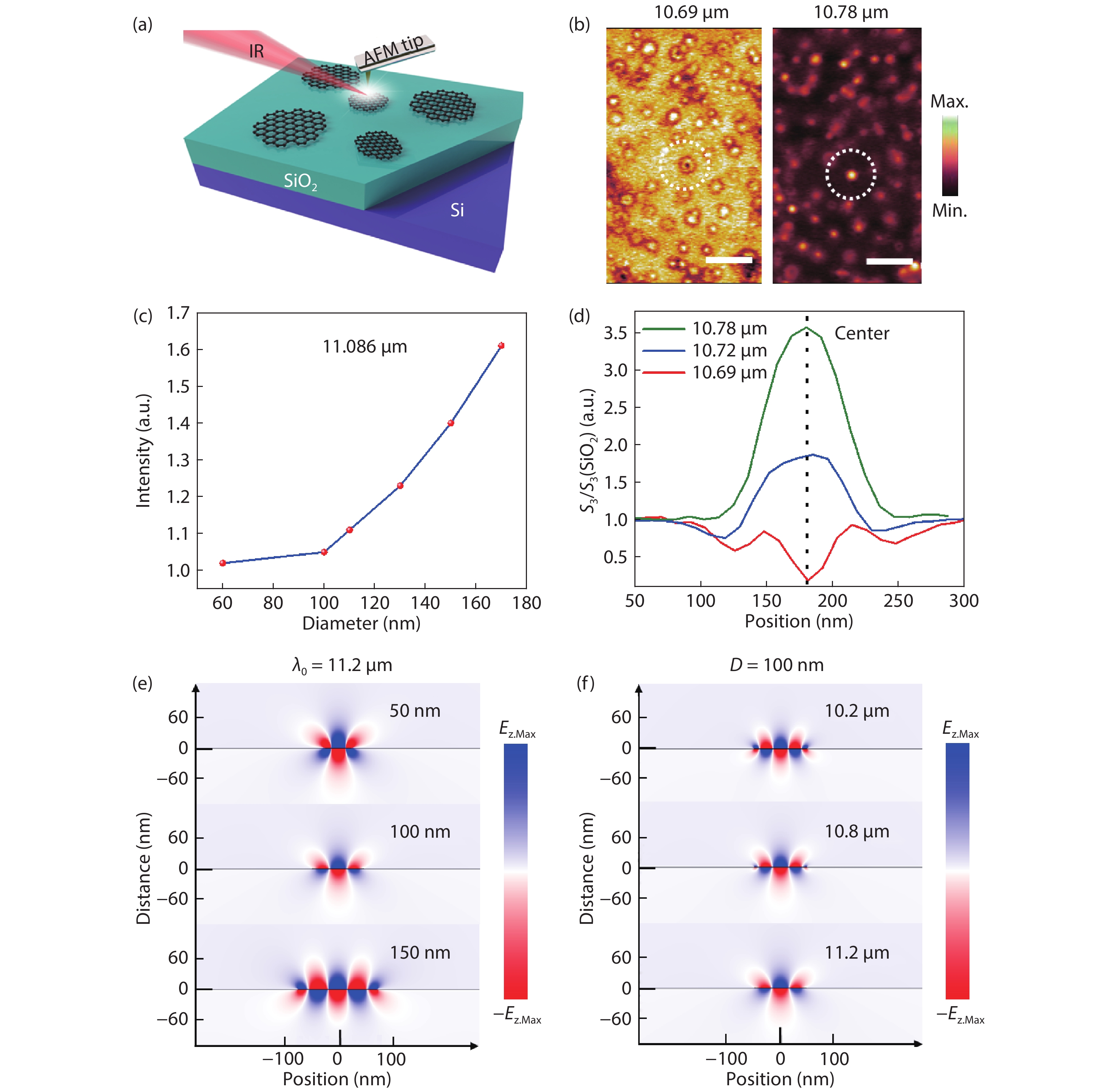
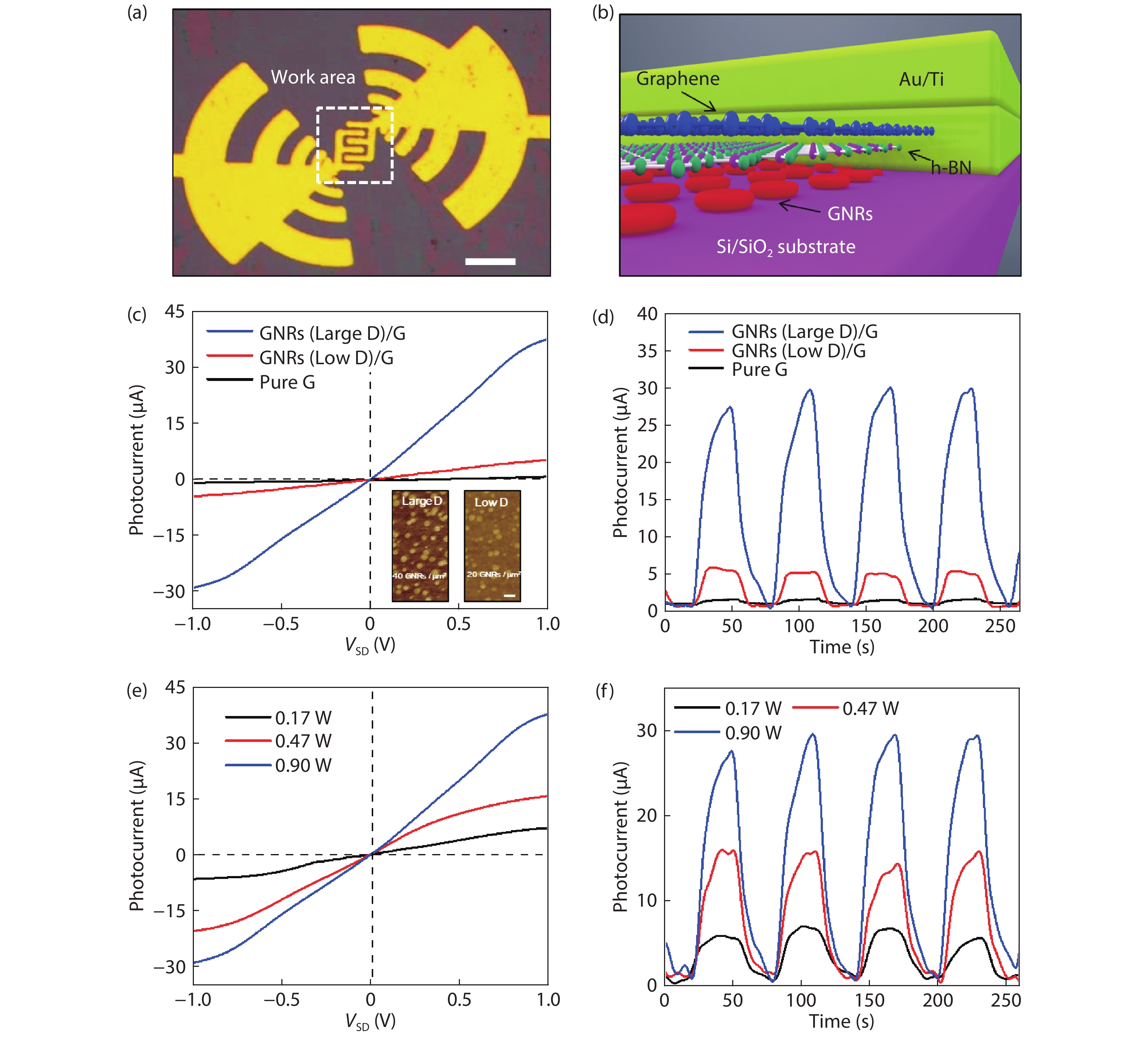
High-performance infrared (IR) photodetectors made by low dimensional materials promise a wide range of applications in communication, security and biomedicine. Moreover, light-harvesting effects based on novel plasmonic materials and their combinations with two-dimensional (2D) materials have raised tremendous interest in recent years, as they may potentially help the device complement or surpass currently commercialized IR photodetectors. Graphene is a particularly attractive plasmonic material because graphene plasmons are electrically tunable with a high degree of electromagnetic confinement in the mid-infrared (mid-IR) to terahertz regime and the field concentration can be further enhanced by forming nanostructures. Here, we report an efficient mid-IR room-temperature photodetector enhanced by plasmonic effect in graphene nanoresonators (GNRs)/graphene heterostructure. The plasmon polaritons in GNRs are size-dependent with strong field localization. Considering that the size and density of GNRs are controllable by chemical vapor deposition method, our work opens a cost-effective and scalable pathway to fabricate efficient IR optoelectronic devices with wavelength tunability.