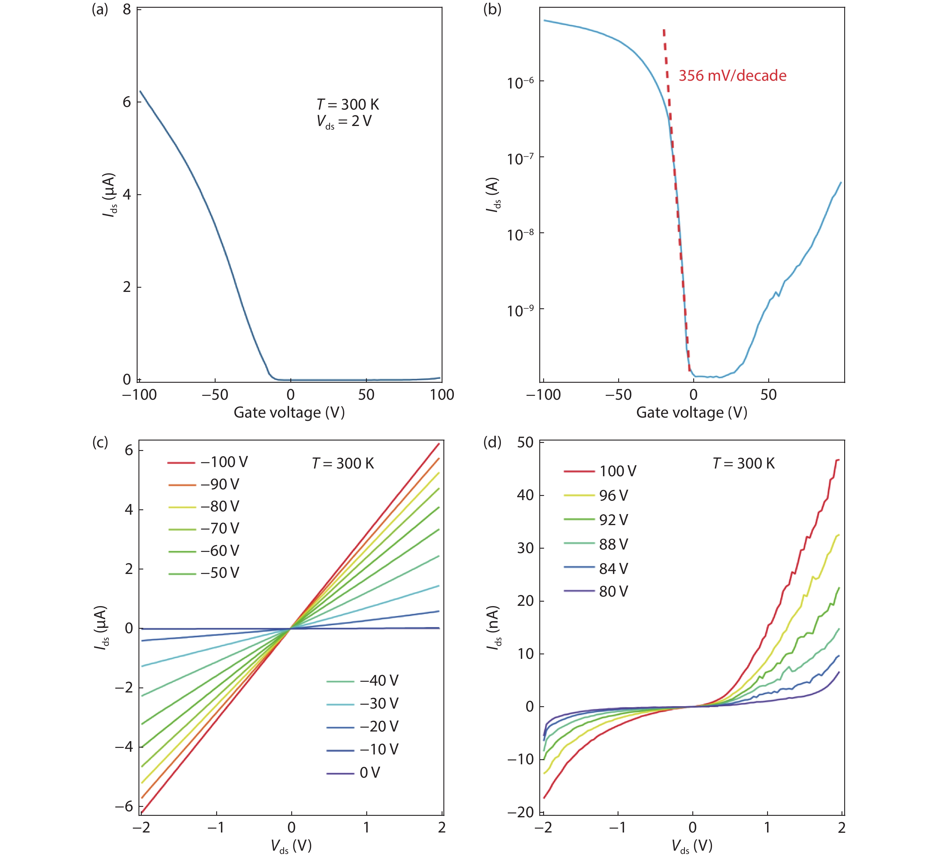
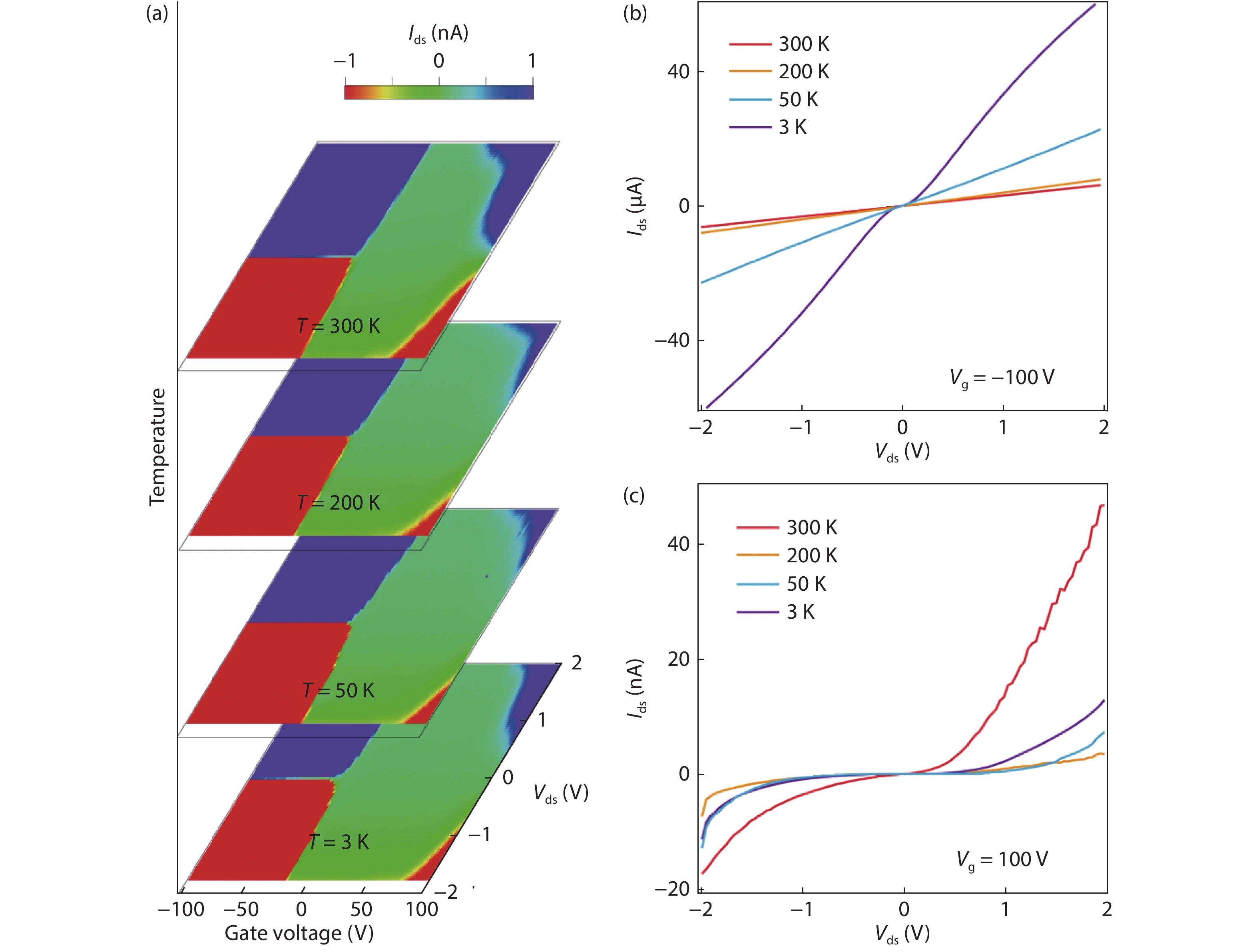
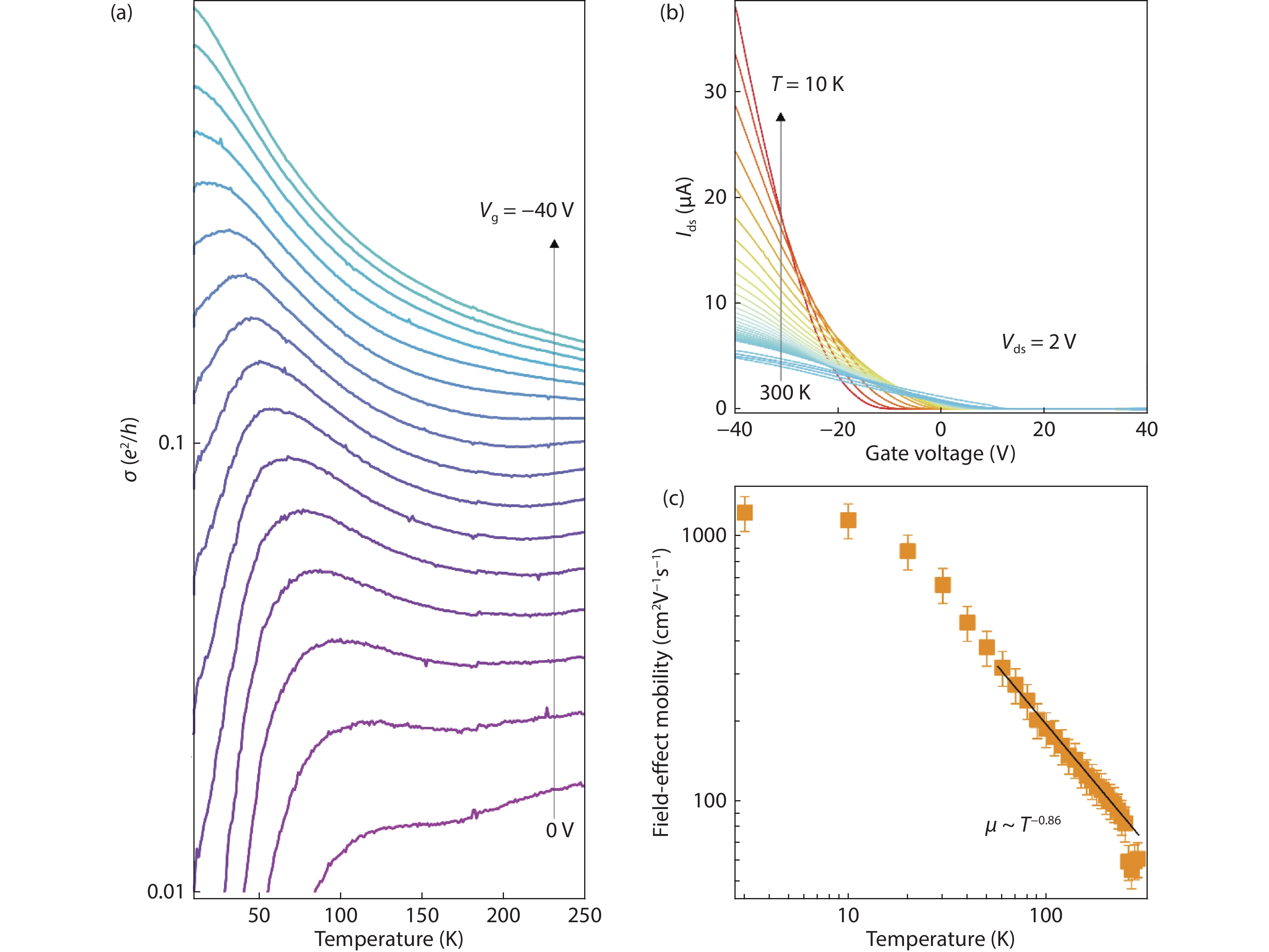
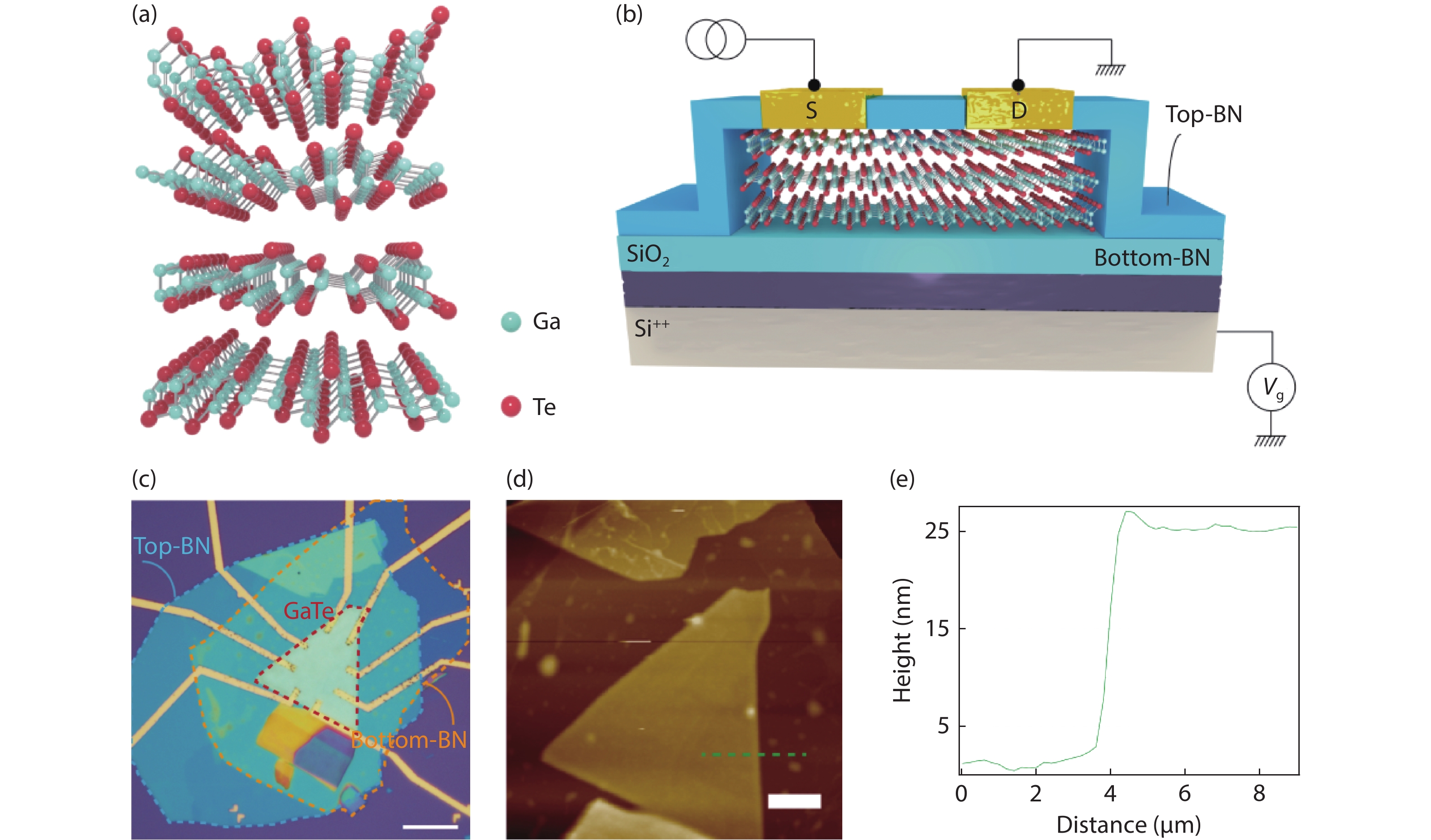
| [1] |
Novoselov K S, Geim A K, Morozov S V, et al. Electric field effect in atomically thin carbon films. Science, 2004, 306(5696), 666 doi: 10.1126/science.1102896 |
| [2] |
Geim A K, Grigorieva I V. Van der Waals heterostructures. Nature, 2013, 499(7459), 419 doi: 10.1038/nature12385 |
| [3] |
Liu Y, Weiss N O, Duan X, et al. Van der Waals heterostructures and devices. Nat Rev Mater, 2016, 1(9), 1 doi: 10.1038/natrevmats.2016.42 |
| [4] |
Saito Y, Iwasa Y. Ambipolar insulator-to-metal transition in black phosphorus by ionic-liquid gating. ACS Nano, 2015, 9(3), 3192 doi: 10.1021/acsnano.5b00497 |
| [5] |
Wang Z, Zhang T, Ding M, et al. Electric-field control of magnetism in a few-layered van der Waals ferromagnetic semiconductor. Nat Nanotechnol, 2018, 13(7), 554 doi: 10.1038/s41565-018-0186-z |
| [6] |
Saito R, Fujita M, Dresselhaus G, et al. Electronic structure of chiral graphene tubules. Appl Phys Lett, 1992, 60(18), 2204 doi: 10.1063/1.107080 |
| [7] |
Mak K F, McGill K L, Park J, et al. The valley Hall effect in MoS 2 transistors. Science, 2014, 344(6191), 1489 doi: 10.1126/science.1250140 |
| [8] |
Huang B, Clark G, Klein D R, et al. Electrical control of 2D magnetism in bilayer CrI 3. Nat Nanotechnol, 2018, 13(7), 544 doi: 10.1038/s41565-018-0121-3 |
| [9] |
Wang X, Tang J, Xia X, et al. Current-driven magnetization switching in a van der Waals ferromagnet Fe 3GeTe 2. Sci Adv, 2019, 5(8), eaaw8904 doi: 10.1126/sciadv.aaw8904 |
| [10] |
|
| [11] |
Kravchenko S, Simonian D, Sarachik M, et al. Electric field scaling at a B = 0 metal-insulator transition in two dimensions. Phys Rev Lett, 1996, 77(24), 4938 doi: 10.1103/PhysRevLett.77.4938 |
| [12] |
Frenzel A J, McLeod A S, Wang D Z R, et al. Infrared nanoimaging of the metal–insulator transition in the charge-density-wave van der Waals material 1T-TaS 2. Phys Rev B, 2018, 97(3), 035111 doi: 10.1103/PhysRevB.97.035111 |
| [13] |
Radisavljevic B, Kis A. Mobility engineering and a metal–insulator transition in monolayer MoS 2. Nat Mater, 2013, 12(9), 815 doi: 10.1038/nmat3687 |
| [14] |
Ponomarenko L, Geim A, Zhukov A, et al. Tunable metal–insulator transition in double-layer graphene heterostructures. Nat Phys, 2011, 7(12), 958 doi: 10.1038/nphys2114 |
| [15] |
Cen C, Thiel S, Hammerl G, et al. Nanoscale control of an interfacial metal–insulator transition at room temperature. Nat Mater, 2008, 7(4), 298 doi: 10.1038/nmat2136 |
| [16] |
Wu C L, Yuan H, Li Y, et al. Gate-induced metal–insulator transition in MoS 2 by solid superionic conductor LaF 3. Nano Lett, 2018, 18(4), 2387 doi: 10.1021/acs.nanolett.7b05377 |
| [17] |
Patil P, Ghosh S, Wasala M, et al. Evidence of metal-insulator transition in 2D Van der Waals layers of copper indium selenide (CuIn7Se11). APS Meeting Abstracts, 2019
|
| [18] |
Duvjir G, Choi B K, Jang I, et al. Emergence of a metal–insulator transition and high-temperature charge-density waves in VSe 2 at the monolayer limit. Nano Lett, 2018, 18(9), 5432 doi: 10.1021/acs.nanolett.8b01764 |
| [19] |
Cao Y, Fatemi V, Fang S, et al. Unconventional superconductivity in magic-angle graphene superlattices. Nature, 2018, 556(7699), 43 doi: 10.1038/nature26160 |
| [20] |
Liu F, Shimotani H, Shang H, et al. High-sensitivity photodetectors based on multilayer GaTe flakes. ACS Nano, 2014, 8(1), 752 doi: 10.1021/nn4054039 |
| [21] |
Huang S, Tatsumi Y, Ling X, et al. In-plane optical anisotropy of layered gallium telluride. ACS Nano, 2016, 10(9), 8964 doi: 10.1021/acsnano.6b05002 |
| [22] |
Kang J, Sangwan V K, Lee H S, et al. Solution-processed layered gallium telluride thin-film photodetectors. ACS Photonics, 2018, 5(10), 3996 doi: 10.1021/acsphotonics.8b01066 |
| [23] |
Wang Z, Safdar M, Mirza M, et al. High-performance flexible photodetectors based on GaTe nanosheets. Nanoscale, 2015, 7(16), 7252 doi: 10.1039/C4NR07313D |
| [24] |
Wang H, Chen M L, Zhu M, et al. Gate tunable giant anisotropic resistance in ultra-thin GaTe. Nat Commun, 2019, 10(1), 1 doi: 10.1038/s41467-018-07882-8 |
| [25] |
Cai H, Chen B, Wang G, et al. Synthesis of highly anisotropic semiconducting GaTe nanomaterials and emerging properties enabled by epitaxy. Adv Mater, 2017, 29(8), 1605551 doi: 10.1002/adma.201605551 |
| [26] |
Wang Z, Xu K, Li Y, et al. Role of Ga vacancy on a multilayer GaTe phototransistor. ACS Nano, 2014, 8(5), 4859 doi: 10.1021/nn500782n |
| [27] |
Castellanos-Gomez A, Buscema M, Molenaar R, et al. Deterministic transfer of two-dimensional materials by all-dry viscoelastic stamping. 2D Mater, 2014, 1(1), 011002 doi: 10.1088/2053-1583/1/1/011002 |
| [28] |
Feng J, Qian X, Huang C W, et al. Strain-engineered artificial atom as a broad-spectrum solar energy funnel. Nat Photonics, 2012, 6(12), 866 doi: 10.1038/nphoton.2012.285 |
| [29] |
Cui Y, Xin R, Yu Z, et al. High-performance monolayer WS 2 field-effect transistors on high- κ dielectrics. Adv Mater, 2015, 27(35), 5230 doi: 10.1002/adma.201502222 |
| [30] |
Movva H C, Rai A, Kang S, et al. High-mobility holes in dual-gated WSe 2 field-effect transistors. ACS Nano, 2015, 9(10), 10402 doi: 10.1021/acsnano.5b04611 |
| [31] |
Radisavljevic B, Radenovic A, Brivio J, et al. Single-layer MoS 2 transistors. Nat Nanotechnol, 2011, 6(3), 147 doi: 10.1038/nnano.2010.279 |
| [32] |
Ovchinnikov D, Allain A, Huang Y S, et al. Electrical transport properties of single-layer WS 2. ACS Nano, 2014, 8(8), 8174 doi: 10.1021/nn502362b |
| [33] |
Dean C R, Young A F, Meric I, et al. Boron nitride substrates for high-quality graphene electronics. Nat Nanotechnol, 2010, 5(10), 722 doi: 10.1038/nnano.2010.172 |


 DownLoad: