


Fig. 1.
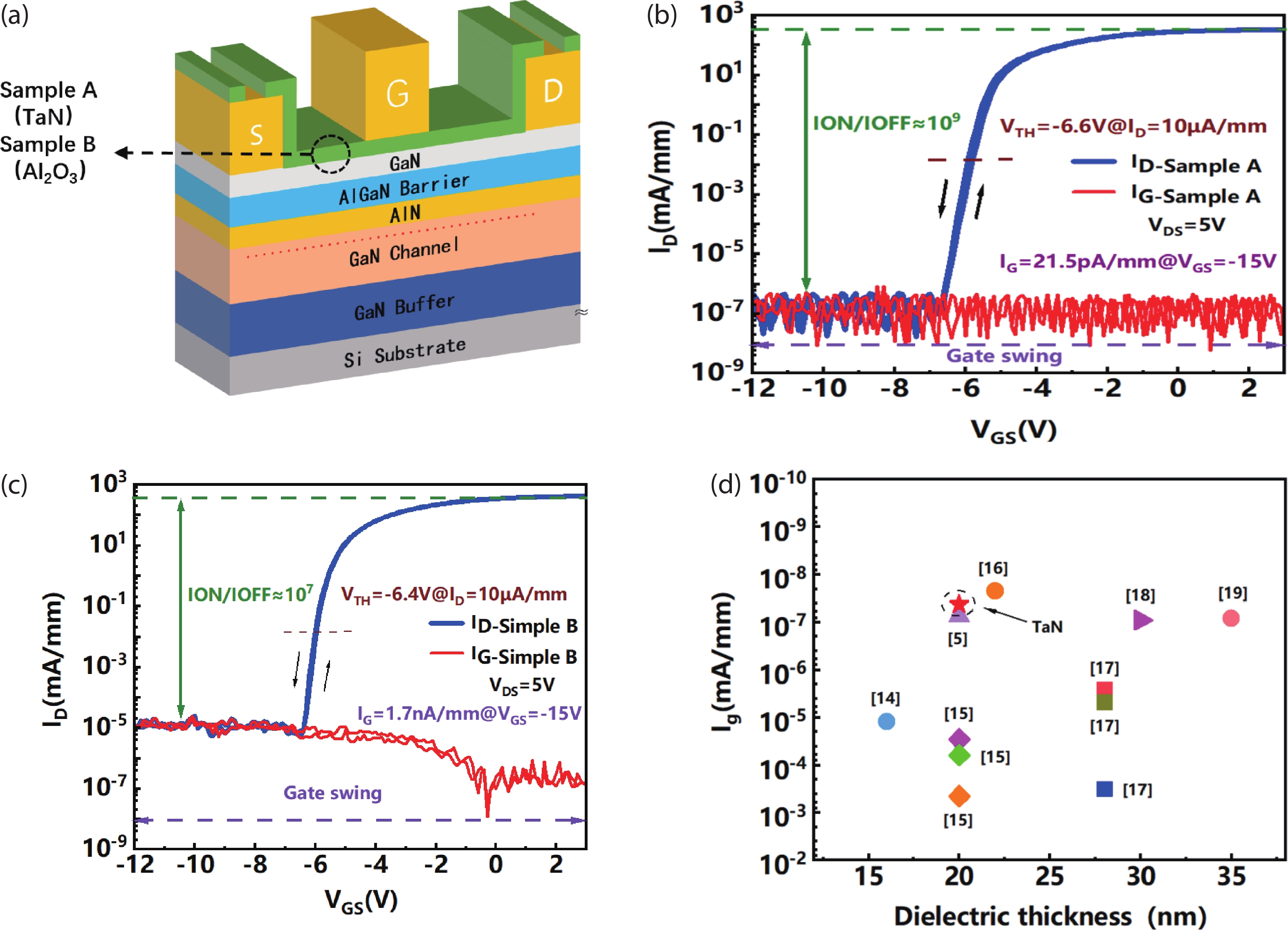
(Color online) (a) Schematic of AlGaN/GaN HEMT with different gate dielectric layers. Logarithmic coordinate transformation curve of (b) Sample A, (c) Sample B. (d) Results of other reported works on leakage current.
ARTICLES
Bosen Liu1, 2, Guohao Yu2, 3, Huimin Jia1, Jingyuan Zhu1, Jiaan Zhou2, Yu Li2, Bingliang Zhang3, Zhongkai Du3, Bohan Guo2, Lu Wang1, Qizhi Huang2, Leifeng Jiang2, Zhongming Zeng2, Zhipeng Wei1, and Baoshun Zhang2,
Corresponding author: Zhipeng Wei, zpweicust@126.com; Baoshun Zhang, bszhang2006@sinano.ac.cn
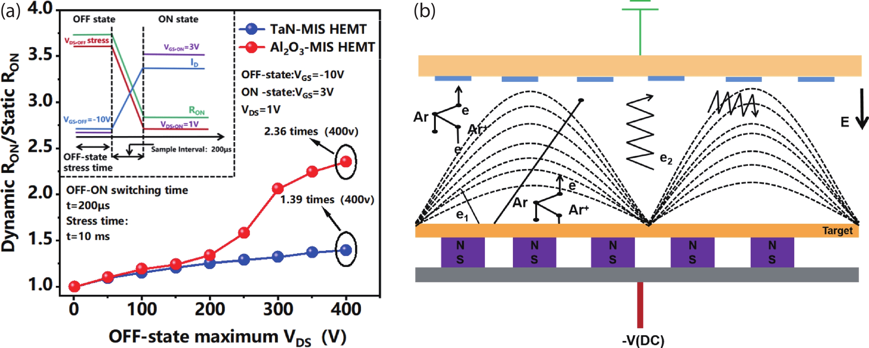
Abstract: In this paper, we explore the electrical characteristics of high-electron-mobility transistors (HEMTs) using a TaN/AlGaN/GaN metal insulating semiconductor (MIS) structure. The high-resistance tantalum nitride (TaN) film prepared by magnetron sputtering as the gate dielectric layer of the device achieved an effective reduction of electronic states at the TaN/AlGaN interface, and reducing the gate leakage current of the MIS HEMT, its performance was enhanced. The HEMT exhibited a low gate leakage current of 2.15 × 10⁻⁷ mA/mm and a breakdown voltage of 1180 V. Furthermore, the MIS HEMT displayed exceptional operational stability during dynamic tests, with dynamic resistance remaining only 1.39 times even under 400 V stress.
Keywords: AlGaN/GaN MIS HEMTs, gate dielectric layer, depletion-mode, gate reliability, Ion/Ioff ratio
| [1] |
Mishra U K, Parikh P, Wu Y F. AlGaN/GaN HEMTs-an overview of device operation and applications. Proceedings of the IEEE, 2002, 90(6), 1022 doi: 10.1109/JPROC.2002.1021567
|
| [2] |
Wang Z, Wang F, Guo S, et al. Simulation study of high-reverse blocking AlGaN/GaN power rectifier with an integrated lateral composite buffer diode. Micro & Nano Letters, 2017, 12(9), 660 doi: 10.1049/mnl.2017.0057
|
| [3] |
Nirmal D, Arivazhagan L, Fletcher A S A, et al. Current collapse modeling in AlGaN/GaN HEMT using small signal equivalent circuit for high power application. Superlattices and Microstructures, 2018, 113, 810 doi: 10.1016/j.spmi.2017.12.027
|
| [4] |
Vetury R, Zhang N Q, Keller S, et al. The impact of surface states on the DC and RF characteristics of AlGaN/GaN HFETs. IEEE Transactions on electron devices, 2001, 48(3), 560 doi: 10.1109/16.906451
|
| [5] |
Deng K, Huang S, Wang X, et al. Insight into the suppression mechanism of bulk traps in Al2O3 gate dielectric and its effect on threshold voltage instability in Al2O3/AlGaN/GaN metal-oxide-semiconductor high electron mobility transistors. Applied Surface Science, 2023, 638, 158000 doi: 10.1016/j.apsusc.2023.158000
|
| [6] |
Huang S, Wang X, Liu X, et al. Interface charge effects on 2-D electron gas in vertical-scaled ultrathin-barrier AlGaN/GaN heterostructure. IEEE Transactions on Electron Devices, 2020, 68(1), 36 doi: 10.1109/TED.2020.3037272
|
| [7] |
Liu Z H, Ng G I, Zhou H, et al. Reduced surface leakage current and trapping effects in AlGaN/GaN high electron mobility transistors on silicon with SiN/Al2O3 passivation. Applied Physics Letters, 2011, 98(11), 3506 doi: 10.1063/1.3567927
|
| [8] |
Van Hove M, Boulay S, Bahl S R, et al. CMOS process-compatible high-power low-leakage AlGaN/GaN MISHEMT on silicon. IEEE Electron Device Letters, 2012, 33(5), 667 doi: 10.1109/LED.2012.2188016
|
| [9] |
Koksaldi O S, Haller J, Li H, et al. N-polar GaN HEMTs exhibiting record breakdown voltage over 2000 V and low dynamic on-resistance. IEEE Electron Device Letters, 2018, 39(7), 1014 doi: 10.1109/LED.2018.2834939
|
| [10] |
Seok O, Ha M W. AlGaN/GaN MOS-HEMTs-on-Si employing sputtered TaN-based electrodes and HfO2 gate insulator. Solid-State Electronics, 2015, 105, 1 doi: 10.1016/j.sse.2014.11.023
|
| [11] |
Baby R, Reshma K, Chandrasekar H, et al. Study of TaN-gated p-GaN E-mode HEMT. IEEE Transactions on Electron Devices, 2023, 70(4), 1607 doi: 10.1109/TED.2023.3241132
|
| [12] |
Yang Z, Fu Z X, Ta S W, et al. Research progress of tantalum nitrogen compound resistance films. Chinese Journal of Vacuum, 2022 doi: 10.13385/j.cnki.vacuum.2022.06.06
|
| [13] |
Stavrev M, Fischer D, Wenzel C, et al. Crystallographic and morphological characterization of reactively sputtered Ta, TaN and TaNO thin films. Thin Solid Films, 1997, 307(1-2), 79 doi: 10.1016/S0040-6090(97)00319-2
|
| [14] |
Ye P D, Yang B, Ng K K, et al. GaN metal-oxide-semiconductor high-electron-mobility-transistor with atomic layer deposited Al2O3 as gate dielectric. Applied Physics Letters, 2005, 86(6), 063501 doi: 10.1063/1.1861122
|
| [15] |
Geng K, Chen D, Zhou Q, et al. AlGaN/GaN MIS-HEMT with PECVD SiNx, SiON, SiO2 as gate dielectric and passivation layer. Electronics, 2018, 7(12), 416 doi: 10.3390/electronics7120416
|
| [16] |
Cai Y, Wang Y, Liang Y, et al. Effect of high-k passivation layer on high voltage properties of GaN metal-insulator-semiconductor devices. IEEE Access, 2020, 8, 95642 doi: 10.1109/ACCESS.2020.2995906
|
| [17] |
Gao S, Zhou Q, Liu X, et al. Breakdown enhancement and current collapse suppression in AlGaN/GaN HEMT by NiOX/SiNX and Al2O3/SiNX as gate dielectric layer and passivation layer. IEEE Electron Device Letters, 2019, 40(12), 1921 doi: 10.1109/LED.2019.2945175
|
| [18] |
Zhao Y P, Wang C, Zheng X F, et al. Ferroelectric effect and equivalent polarization charge model of PbZr0.2Ti0.8O3 on AlGaN/GaN MIS-HEMT. Chinese Physics B, 2021, 30(5), 057302 doi: 10.1088/1674-1056/abd469
|
| [19] |
Que T T, Zhao Y W, Qiu Q L, et al. Evaluation of stress voltage on off-state time-dependent breakdown for GaN MIS-HEMT with SiNx gate dielectric. Chinese Physics B, 2020, 29(10), 107201 doi: 10.1088/1674-1056/abaed8
|
| [20] |
Huang S, Liu X, Wei K, et al. O3-sourced atomic layer deposition of high quality Al2O3 gate dielectric for normally-off GaN metal-insulator-semiconductor high-electron-mobility transistors. Applied Physics Letters, 2015, 106(3), 3507 doi: 10.1063/1.4906601
|
| [21] |
Deng K, Wang X, Huang S, et al. Effective suppression of deep interface states and dielectric trapping in SiNx/GaN metal-insulator-semiconductor structures by a SiOxNy interfacial layer grown by plasma-enhanced atomic layer deposition. Applied Surface Science, 2023, 607, 154937 doi: 10.1016/j.apsusc.2022.154937
|
| [22] |
Hua M, Cai X, Yang S, et al. Enhanced gate reliability in GaN MIS-FETs by converting the GaN channel into crystalline gallium oxynitride. ACS Applied Electronic Materials, 2019, 1(5), 642 doi: 10.1021/acsaelm.8b00102
|
| [23] |
Yu C, Ding G, Feng Q, et al. An AlGaN/GaN HEMT with sputter-SiN passivation for the on-state performance improvement. Micro and Nanostructures, 2022, 168, 207316 doi: 10.1016/j.micrna.2022.207316
|
| [24] |
Chen C, Wang Q, Li W, et al. Effect of the post-gate annealing on the gate reliability of AlGaN/GaN HEMTs. Journal of Semiconductors, 2021, 42(9), 092802 doi: 10.1088/1674-4926/42/9/092802
|
| [25] |
Duan B X, Yang Y T. Breakdown voltage analysis for the new RESURF AlGaN/GaN HEMTs. Science China Information Sciences, 2012, 55, 473 doi: 10.1007/s11432-011-4496-0
|
| [26] |
Natarajan R. Enhancement of blocking voltage in GaN HEMT using stacked passivation layer. Silicon, 2022, 14(14), 8487 doi: 10.1007/s12633-021-01646-8
|
| [27] |
Koehler A D, Nepal N, Anderson T J, et al. Atomic layer epitaxy AlN for enhanced AlGaN/GaN HEMT passivation. IEEE electron device letters, 2013, 34(9), 1115 doi: 10.1109/LED.2013.2274429
|
| [28] |
Kim H, Lee J, Liu D, et al. Gate current leakage and breakdown mechanism in unpassivated AlGaN∕GaN high electron mobility transistors by post-gate annealing. Applied Physics Letters, 2005, 86, 143505 doi: 10.1063/1.1899255
|
| [29] |
Sun R, Liang Y C, Yeo Y C, et al. Realistic trap configuration scheme with fabrication processes in consideration for the simulations of AlGaN/GaN MIS-HEMT devices. IEEE Journal of Emerging and Selected Topics in Power Electronics, 2016, 4(3), 720 doi: 10.1109/JESTPE.2016.2549959
|
| [30] |
Chan C Y, Lee T C, Hsu S S H, et al. Impacts of gate recess and passivation on AlGaN/GaN high electron mobility transistors. Japanese Journal of Applied Physics, 2007, 46(2R), 478 doi: 10.1143/JJAP.46.478
|
| [31] |
Germain M, Leys M, Derluyn J, et al. Surface stabilization for higher performance AlGaN/GaN HEMT with in-situ MOVPE SiN. MRS Online Proceedings Library (OPL), 2004, 831, E6 doi: 10.1557/PROC-831-E6.7
|
| [32] |
Wang J, Pedroza L S, Poissier A, et al. Water dissociation at the GaN (1010) surface: Structure, dynamics and surface acidity. The Journal of Physical Chemistry C, 2012, 116(27), 14382 doi: 10.1021/jp302793s
|
| [33] |
Hu Q, Li S, Li T, et al. Channel engineering of normally-OFF AlGaN/GaN MOS-HEMTs by atomic layer etching and high-k dielectric. IEEE Electron Device Letters, 2018, 39(9), 1377 doi: 10.1109/LED.2018.2856934
|
| [34] |
Yang S, Liu S, Lu Y, et al. AC-capacitance techniques for interface trap analysis in GaN-based buried-channel MIS-HEMTs. IEEE Transactions on Electron Devices, 2015, 62(6), 1870 doi: 10.1109/TED.2015.2420690
|
| [35] |
Lin Y S, Lain Y W, Hsu S S H. AlGaN/GaN HEMTs with low leakage current and high on/off current ratio. IEEE Electron Device Letters, 2009, 31(2), 102 doi: 10.1109/LED.2009.2036576
|


Article views: 3431 Times PDF downloads: 313 Times Cited by: 0 Times
Received: 22 January 2024 Revised: 18 February 2024 Online: Uncorrected proof: 31 March 2024Accepted Manuscript: 31 March 2024Published: 15 July 2024
| Citation: |
Bosen Liu, Guohao Yu, Huimin Jia, Jingyuan Zhu, Jiaan Zhou, Yu Li, Bingliang Zhang, Zhongkai Du, Bohan Guo, Lu Wang, Qizhi Huang, Leifeng Jiang, Zhongming Zeng, Zhipeng Wei, Baoshun Zhang. Current-collapse suppression and leakage-current decrease in AlGaN/GaN HEMT by sputter-TaN gate-dielectric layer[J]. Journal of Semiconductors, 2024, 45(7): 072501. doi: 10.1088/1674-4926/24010025
****
B S Liu, G H Yu, H M Jia, J Y Zhu, J A Zhou, Y Li, B L Zhang, Z K Du, B H Guo, L Wang, Q Z Huang, L F Jiang, Z M Zeng, Z P Wei, and B S Zhang, Current-collapse suppression and leakage-current decrease in AlGaN/GaN HEMT by sputter-TaN gate-dielectric layer[J]. J. Semicond., 2024, 45(7), 072501 doi: 10.1088/1674-4926/24010025

|
 Bosen Liu received his BS degree from Changchun Electronic Science and Technology Institute in 2021. He is now an MS student at Changchun University of Science and Technology. His research focuses on the optimization of performance and reliability for GaN HEMT devices
 Baoshun Zhang received his BS degree from Changchun University of Science and Technology in 1994 and his PhD degree from the Institute of Semiconductors, Chinese Academy of Sciences in 2003. Then he joined in Hong Kong University of Science and Technology. Currently, he is a researcher at Suzhou Institute of Nano-Tech and Nano-Bionics, Chinese Academy of Sciences, and his research interests include semiconductor material growth and device technology research
| [1] |
Mishra U K, Parikh P, Wu Y F. AlGaN/GaN HEMTs-an overview of device operation and applications. Proceedings of the IEEE, 2002, 90(6), 1022 doi: 10.1109/JPROC.2002.1021567
|
| [2] |
Wang Z, Wang F, Guo S, et al. Simulation study of high-reverse blocking AlGaN/GaN power rectifier with an integrated lateral composite buffer diode. Micro & Nano Letters, 2017, 12(9), 660 doi: 10.1049/mnl.2017.0057
|
| [3] |
Nirmal D, Arivazhagan L, Fletcher A S A, et al. Current collapse modeling in AlGaN/GaN HEMT using small signal equivalent circuit for high power application. Superlattices and Microstructures, 2018, 113, 810 doi: 10.1016/j.spmi.2017.12.027
|
| [4] |
Vetury R, Zhang N Q, Keller S, et al. The impact of surface states on the DC and RF characteristics of AlGaN/GaN HFETs. IEEE Transactions on electron devices, 2001, 48(3), 560 doi: 10.1109/16.906451
|
| [5] |
Deng K, Huang S, Wang X, et al. Insight into the suppression mechanism of bulk traps in Al2O3 gate dielectric and its effect on threshold voltage instability in Al2O3/AlGaN/GaN metal-oxide-semiconductor high electron mobility transistors. Applied Surface Science, 2023, 638, 158000 doi: 10.1016/j.apsusc.2023.158000
|
| [6] |
Huang S, Wang X, Liu X, et al. Interface charge effects on 2-D electron gas in vertical-scaled ultrathin-barrier AlGaN/GaN heterostructure. IEEE Transactions on Electron Devices, 2020, 68(1), 36 doi: 10.1109/TED.2020.3037272
|
| [7] |
Liu Z H, Ng G I, Zhou H, et al. Reduced surface leakage current and trapping effects in AlGaN/GaN high electron mobility transistors on silicon with SiN/Al2O3 passivation. Applied Physics Letters, 2011, 98(11), 3506 doi: 10.1063/1.3567927
|
| [8] |
Van Hove M, Boulay S, Bahl S R, et al. CMOS process-compatible high-power low-leakage AlGaN/GaN MISHEMT on silicon. IEEE Electron Device Letters, 2012, 33(5), 667 doi: 10.1109/LED.2012.2188016
|
| [9] |
Koksaldi O S, Haller J, Li H, et al. N-polar GaN HEMTs exhibiting record breakdown voltage over 2000 V and low dynamic on-resistance. IEEE Electron Device Letters, 2018, 39(7), 1014 doi: 10.1109/LED.2018.2834939
|
| [10] |
Seok O, Ha M W. AlGaN/GaN MOS-HEMTs-on-Si employing sputtered TaN-based electrodes and HfO2 gate insulator. Solid-State Electronics, 2015, 105, 1 doi: 10.1016/j.sse.2014.11.023
|
| [11] |
Baby R, Reshma K, Chandrasekar H, et al. Study of TaN-gated p-GaN E-mode HEMT. IEEE Transactions on Electron Devices, 2023, 70(4), 1607 doi: 10.1109/TED.2023.3241132
|
| [12] |
Yang Z, Fu Z X, Ta S W, et al. Research progress of tantalum nitrogen compound resistance films. Chinese Journal of Vacuum, 2022 doi: 10.13385/j.cnki.vacuum.2022.06.06
|
| [13] |
Stavrev M, Fischer D, Wenzel C, et al. Crystallographic and morphological characterization of reactively sputtered Ta, TaN and TaNO thin films. Thin Solid Films, 1997, 307(1-2), 79 doi: 10.1016/S0040-6090(97)00319-2
|
| [14] |
Ye P D, Yang B, Ng K K, et al. GaN metal-oxide-semiconductor high-electron-mobility-transistor with atomic layer deposited Al2O3 as gate dielectric. Applied Physics Letters, 2005, 86(6), 063501 doi: 10.1063/1.1861122
|
| [15] |
Geng K, Chen D, Zhou Q, et al. AlGaN/GaN MIS-HEMT with PECVD SiNx, SiON, SiO2 as gate dielectric and passivation layer. Electronics, 2018, 7(12), 416 doi: 10.3390/electronics7120416
|
| [16] |
Cai Y, Wang Y, Liang Y, et al. Effect of high-k passivation layer on high voltage properties of GaN metal-insulator-semiconductor devices. IEEE Access, 2020, 8, 95642 doi: 10.1109/ACCESS.2020.2995906
|
| [17] |
Gao S, Zhou Q, Liu X, et al. Breakdown enhancement and current collapse suppression in AlGaN/GaN HEMT by NiOX/SiNX and Al2O3/SiNX as gate dielectric layer and passivation layer. IEEE Electron Device Letters, 2019, 40(12), 1921 doi: 10.1109/LED.2019.2945175
|
| [18] |
Zhao Y P, Wang C, Zheng X F, et al. Ferroelectric effect and equivalent polarization charge model of PbZr0.2Ti0.8O3 on AlGaN/GaN MIS-HEMT. Chinese Physics B, 2021, 30(5), 057302 doi: 10.1088/1674-1056/abd469
|
| [19] |
Que T T, Zhao Y W, Qiu Q L, et al. Evaluation of stress voltage on off-state time-dependent breakdown for GaN MIS-HEMT with SiNx gate dielectric. Chinese Physics B, 2020, 29(10), 107201 doi: 10.1088/1674-1056/abaed8
|
| [20] |
Huang S, Liu X, Wei K, et al. O3-sourced atomic layer deposition of high quality Al2O3 gate dielectric for normally-off GaN metal-insulator-semiconductor high-electron-mobility transistors. Applied Physics Letters, 2015, 106(3), 3507 doi: 10.1063/1.4906601
|
| [21] |
Deng K, Wang X, Huang S, et al. Effective suppression of deep interface states and dielectric trapping in SiNx/GaN metal-insulator-semiconductor structures by a SiOxNy interfacial layer grown by plasma-enhanced atomic layer deposition. Applied Surface Science, 2023, 607, 154937 doi: 10.1016/j.apsusc.2022.154937
|
| [22] |
Hua M, Cai X, Yang S, et al. Enhanced gate reliability in GaN MIS-FETs by converting the GaN channel into crystalline gallium oxynitride. ACS Applied Electronic Materials, 2019, 1(5), 642 doi: 10.1021/acsaelm.8b00102
|
| [23] |
Yu C, Ding G, Feng Q, et al. An AlGaN/GaN HEMT with sputter-SiN passivation for the on-state performance improvement. Micro and Nanostructures, 2022, 168, 207316 doi: 10.1016/j.micrna.2022.207316
|
| [24] |
Chen C, Wang Q, Li W, et al. Effect of the post-gate annealing on the gate reliability of AlGaN/GaN HEMTs. Journal of Semiconductors, 2021, 42(9), 092802 doi: 10.1088/1674-4926/42/9/092802
|
| [25] |
Duan B X, Yang Y T. Breakdown voltage analysis for the new RESURF AlGaN/GaN HEMTs. Science China Information Sciences, 2012, 55, 473 doi: 10.1007/s11432-011-4496-0
|
| [26] |
Natarajan R. Enhancement of blocking voltage in GaN HEMT using stacked passivation layer. Silicon, 2022, 14(14), 8487 doi: 10.1007/s12633-021-01646-8
|
| [27] |
Koehler A D, Nepal N, Anderson T J, et al. Atomic layer epitaxy AlN for enhanced AlGaN/GaN HEMT passivation. IEEE electron device letters, 2013, 34(9), 1115 doi: 10.1109/LED.2013.2274429
|
| [28] |
Kim H, Lee J, Liu D, et al. Gate current leakage and breakdown mechanism in unpassivated AlGaN∕GaN high electron mobility transistors by post-gate annealing. Applied Physics Letters, 2005, 86, 143505 doi: 10.1063/1.1899255
|
| [29] |
Sun R, Liang Y C, Yeo Y C, et al. Realistic trap configuration scheme with fabrication processes in consideration for the simulations of AlGaN/GaN MIS-HEMT devices. IEEE Journal of Emerging and Selected Topics in Power Electronics, 2016, 4(3), 720 doi: 10.1109/JESTPE.2016.2549959
|
| [30] |
Chan C Y, Lee T C, Hsu S S H, et al. Impacts of gate recess and passivation on AlGaN/GaN high electron mobility transistors. Japanese Journal of Applied Physics, 2007, 46(2R), 478 doi: 10.1143/JJAP.46.478
|
| [31] |
Germain M, Leys M, Derluyn J, et al. Surface stabilization for higher performance AlGaN/GaN HEMT with in-situ MOVPE SiN. MRS Online Proceedings Library (OPL), 2004, 831, E6 doi: 10.1557/PROC-831-E6.7
|
| [32] |
Wang J, Pedroza L S, Poissier A, et al. Water dissociation at the GaN (1010) surface: Structure, dynamics and surface acidity. The Journal of Physical Chemistry C, 2012, 116(27), 14382 doi: 10.1021/jp302793s
|
| [33] |
Hu Q, Li S, Li T, et al. Channel engineering of normally-OFF AlGaN/GaN MOS-HEMTs by atomic layer etching and high-k dielectric. IEEE Electron Device Letters, 2018, 39(9), 1377 doi: 10.1109/LED.2018.2856934
|
| [34] |
Yang S, Liu S, Lu Y, et al. AC-capacitance techniques for interface trap analysis in GaN-based buried-channel MIS-HEMTs. IEEE Transactions on Electron Devices, 2015, 62(6), 1870 doi: 10.1109/TED.2015.2420690
|
| [35] |
Lin Y S, Lain Y W, Hsu S S H. AlGaN/GaN HEMTs with low leakage current and high on/off current ratio. IEEE Electron Device Letters, 2009, 31(2), 102 doi: 10.1109/LED.2009.2036576
|

 WeChat ID
Journal of Semiconductors © 2017 All Rights Reserved 京ICP备05085259号-2

 DownLoad:

