


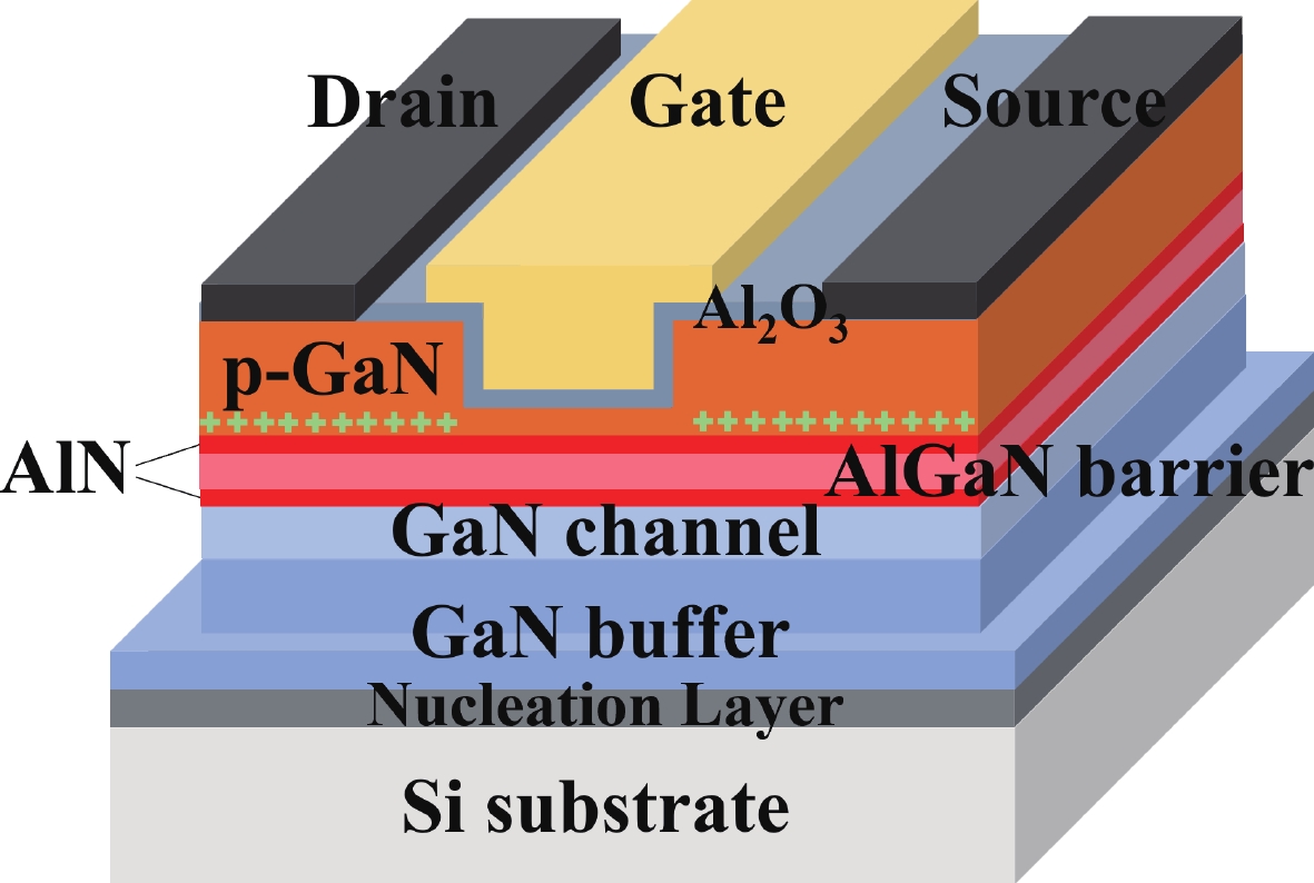
Fig. 1.
(Color online) Cross-sectional schematic of the fabricated GaN E-Mode PMOS.
ARTICLES
Huake Su1, Tao Zhang1, , Shengrui Xu1, , Hongchang Tao1, Yibo Wang2, Yuan Gao1, Yue Hao1 and Jincheng Zhang1,
Corresponding author: Tao Zhang, zhangtao@xidian.edu.cn; Shengrui Xu, shengruixidian@126.com; Jincheng Zhang, jchzhang@xidian.edu.cn
Abstract: Pre-ohmic-annealing (POA) treatment of P-GaN/AlN/AlGaN epitaxy under N2 atmosphere was demonstrated to effectively achieve good p-type ohmic contact as well as decreased epitaxy sheet resistance. Ohmic contact resistance (Rc) extracted by transfer length method reduced from 38 to 23 Ω·mm with alleviated contact barrier height from 0.55 to 0.51 eV after POA treatment. X-ray photoelectron spectroscopy and Hall measurement confirmed that POA treatment was able to reduce surface state density and improve the hole concentration of p-GaN. Due to the decreased Rc and improved two-dimensional hole gas (2DHG) density, an outstanding-performance GaN E-mode p-channel MOSFET was successfully realized.
Keywords: POA treatment, GaN, p-channel, E-Mode, barrier height, surface states
| [1] |
Tao H C, Xu S R, Zhang J C, et al. Improved crystal quality and enhanced optical performance of GaN enabled by ion implantation induced high-quality nucleation. Opt Express, 2023, 31, 20850 doi: 10.1364/OE.492088
|
| [2] |
Peng R S, Xu S R, Fan X M, et al. Application of nano-patterned InGaN fabricated by self-assembled Ni nano-masks in green InGaN/GaN multiple quantum wells. J Semicond, 2023, 44, 042801 doi: 10.1088/1674-4926/44/4/042801
|
| [3] |
Zhang T, Zhang J C, Zhou H, et al. A > 3 kV/2.94 mΩ·cm2 and low leakage current with low turn-on voltage lateral GaN Schottky barrier diode on silicon substrate with anode engineering technique. IEEE Electron Device Lett, 2019, 40, 1583 doi: 10.1109/LED.2019.2933314
|
| [4] |
Smorchkova I P, Elsass C R, Ibbetson J P, et al. Polarization-induced charge and electron mobility in AlGaN/GaN heterostructures grown by plasma-assisted molecular-beam epitaxy. J Appl Phys, 1999, 86, 4520 doi: 10.1063/1.371396
|
| [5] |
Cai Y, Zhou Y G, Chen K J, et al. High-performance enhancement-mode AlGaN/GaN HEMTs using fluoride-based plasma treatment. IEEE Electron Device Lett, 2005, 26, 435 doi: 10.1109/LED.2005.851122
|
| [6] |
Tang Z K, Jiang Q M, Lu Y Y, et al. 600-V normally off SiNx/AlGaN/GaN MIS-HEMT with large gate swing and low current collapse. IEEE Electron Device Lett, 2013, 34, 1373 doi: 10.1109/LED.2013.2279846
|
| [7] |
Zheng Z Y, Zhang L, Song W J, et al. Gallium nitride-based complementary logic integrated circuits. Nat Electron, 2021, 4, 595 doi: 10.1038/s41928-021-00611-y
|
| [8] |
Du H H, Liu Z H, Hao L, et al. High-performance E-mode p-channel GaN FinFET on silicon substrate with high ION/IOFF and high threshold voltage. IEEE Electron Device Lett, 2022, 43, 705 doi: 10.1109/LED.2022.3155152
|
| [9] |
Chowdhury N, Lemettinen J, Xie Q Y, et al. P-channel GaN transistor based on p-GaN/AlGaN/GaN on Si. IEEE Electron Device Lett, 2019, 40, 1036 doi: 10.1109/LED.2019.2916253
|
| [10] |
Yang C, Fu H Q, Peri P, et al. Enhancement-mode gate-recess-free GaN-based p-channel heterojunction field-effect transistor with ultra-low subthreshold swing. IEEE Electron Device Lett, 2021, 42, 1128 doi: 10.1109/LED.2021.3092040
|
| [11] |
Chowdhury N, Xie Q Y, Yuan M Y, et al. First demonstration of a self-aligned GaN p-FET. 2019 IEEE International Electron Devices Meeting (IEDM), 2019, 4.6. 1
|
| [12] |
Chowdhury N, Xie Q Y, Niroula J, et al. Field-induced acceptor ionization in enhancement-mode GaN p-MOSFETs. 2020 IEEE International Electron Devices Meeting (IEDM), 2020, 5.5. 12
|
| [13] |
Chowdhury N, Xie Q Y, Palacios T. Self-aligned E-mode GaN p-channel FinFET with ION > 100 mA/mm and ION/IOFF > 107. IEEE Electron Device Lett, 2022, 43, 358 doi: 10.1109/LED.2022.3140281
|
| [14] |
Nomoto K, Chaudhuri R, Bader S J, et al. GaN/AlN p-channel HFETs with Imax >420 mA/mm and ~20 GHz fT/fMAX. 2020 IEEE International Electron Devices Meeting (IEDM), 2020, 8.3. 1
|
| [15] |
Raj A, Krishna A, Hatui N, et al. GaN/AlGaN superlattice based E-mode p-channel MES-FinFET with regrown contacts and >50 mA/mm on-current. 2021 IEEE International Electron Devices Meeting (IEDM), 2021, 5.4. 1
|
| [16] |
Raj A, Krishna A, Romanczyk B, et al. GaN/AlGaN superlattice based E-mode hole channel FinFET with Schottky gate. IEEE Electron Device Lett, 2023, 44, 9 doi: 10.1109/LED.2022.3223331
|
| [17] |
Chowdhury N, Xie Q Y, Yuan M Y, et al. Regrowth-free GaN-based complementary logic on a Si substrate. IEEE Electron Device Lett, 2020, 41, 820 doi: 10.1109/LED.2020.2987003
|
| [18] |
Bader S J, Chaudhuri R, Nomoto K, et al. Gate-recessed E-mode p-channel HFET with high on-current based on GaN/AlN 2D hole gas. IEEE Electron Device Lett, 2018, 39, 1848 doi: 10.1109/LED.2018.2874190
|
| [19] |
Götz W, Johnson N M, Walker J, et al. Activation of acceptors in Mg-doped GaN grown by metalorganic chemical vapor deposition. Appl Phys Lett, 1996, 68, 667 doi: 10.1063/1.116503
|
| [20] |
Zhang G Y, Tong Y Z, Yang Z J, et al. Relationship of background carrier concentration and defects in GaN grown by metalorganic vapor phase epitaxy. Appl Phys Lett, 1997, 71, 3376 doi: 10.1063/1.120341
|
| [21] |
Cao X A, Pearton S J, Zhang A P, et al. Electrical effects of plasma damage in p-GaN. Appl Phys Lett, 1999, 75, 2569 doi: 10.1063/1.125080
|
| [22] |
Foster G M, Koehler A, Ebrish M, et al. Recovery from plasma etching-induced nitrogen vacancies in p-type gallium nitride using UV/O3 treatments. Appl Phys Lett, 2020, 117, 082103 doi: 10.1063/5.0021153
|
| [23] |
Bader S J, Chaudhuri R, Hickman A, et al. GaN/AlN Schottky-gate p-channel HFETs with InGaN contacts and 100 mA/mm on-current. 2019 IEEE International Electron Devices Meeting (IEDM), 2019, 4.5. 1
|
| [24] |
Lu S, Deki M, Wang J, et al. Ohmic contact on low-doping-density p-type GaN with nitrogen-annealed Mg. Appl Phys Lett, 2021, 119, 242104 doi: 10.1063/5.0076764
|
| [25] |
Wang J, Lu S, Cai W T, et al. Ohmic contact to p-type GaN enabled by post-growth diffusion of magnesium. IEEE Electron Device Lett, 2022, 43, 150 doi: 10.1109/LED.2021.3131057
|
| [26] |
Tang C Y, Lu H H, Qiao Z P, et al. Ohmic contact with a contact resistivity of 12 Ω·mm on p-GaN/AlGaN/GaN. IEEE Electron Device Lett, 2022, 43, 1412 doi: 10.1109/LED.2022.3193004
|
| [27] |
Su H K, Zhang T, Xu S R, et al. Mechanism of low Ohmic contact resistance to p-type GaN by suppressed edge dislocations. Appl Phys Lett, 2022, 120, 222101 doi: 10.1063/5.0090693
|
| [28] |
Wenzel R, Fischer G G, Schmid-Fetzer R. Ohmic contacts on p-GaN (Part I). Mater Sci Semicond Process, 2001, 4, 357 doi: 10.1016/S1369-8001(00)00177-3
|
| [29] |
Kalaitzakis F G, Pelekanos N T, Prystawko P, et al. Low resistance as-deposited Cr/Au contacts on p-type GaN. Appl Phys Lett, 2007, 91, 261103 doi: 10.1063/1.2828044
|
| [30] |
Pan S, Lu Y M, Liang Z B, et al. Optimization of annealing conditions for Ag/p-GaN ohmic contacts. Appl Phys A Mater Sci Process, 2021, 127, 870 doi: 10.1007/s00339-021-05022-6
|
| [31] |
Wahid S, Chowdhury N, Alam M K, et al. Barrier heights and Fermi level pinning in metal contacts on p-type GaN. Appl Phys Lett, 2020, 116, 213506 doi: 10.1063/5.0010699
|
| [32] |
Kim J K, Lee J L, Lee J W, et al. Low resistance Pd/Au ohmic contacts to p-type GaN using surface treatment. Appl Phys Lett, 1998, 73, 2953 doi: 10.1063/1.122641
|
| [33] |
Lee J L, Kim J K, Lee J W, et al. Effect of surface treatment by KOH solution on ohmic contact formation of p-type GaN. Solid State Electron, 1999, 43, 435 doi: 10.1016/S0038-1101(98)00265-2
|
| [34] |
Mori T, Kozawa T, Ohwaki T, et al. Schottky barriers and contact resistances on p-type GaN. Appl Phys Lett, 1996, 69, 3537 doi: 10.1063/1.117237
|
| [35] |
Pankove J I, Torvik J T, Qiu C H, et al. Molecular doping of gallium nitride. Appl Phys Lett, 1999, 74, 416 doi: 10.1063/1.123046
|
| [36] |
Wright A F. Substitutional and interstitial oxygen in wurtzite GaN. J Appl Phys, 2005, 98, 103531 doi: 10.1063/1.2137446
|
| [37] |
Arslan I, Browning N D. Role of oxygen at screw dislocations in GaN. Phys Rev Lett, 2003, 91, 165501 doi: 10.1103/PhysRevLett.91.165501
|
| [38] |
Zywietz T K, Neugebauer J, Scheffler M. The adsorption of oxygen at GaN surfaces. Appl Phys Lett, 1999, 74, 1695 doi: 10.1063/1.123658
|
| [39] |
Pearton S J, Cho H, LaRoche J R, et al. Oxygen diffusion into SiO2-capped GaN during annealing. Appl Phys Lett, 1999, 75, 2939 doi: 10.1063/1.125194
|
| [40] |
Huang B R, Chou C H, Ke W C, et al. Effects of hydrogen treatment on ohmic contacts to p-type GaN films. Appl Surf Sci, 2011, 257, 7490 doi: 10.1016/j.apsusc.2011.03.061
|
| [41] |
Reuters B, Hahn H, Pooth A, et al. Fabrication of p-channel heterostructure field effect transistors with polarization-induced two-dimensional hole gases at metal-polar GaN/AlInGaN interfaces. J Phys D Appl Phys, 2014, 47, 175103 doi: 10.1088/0022-3727/47/17/175103
|
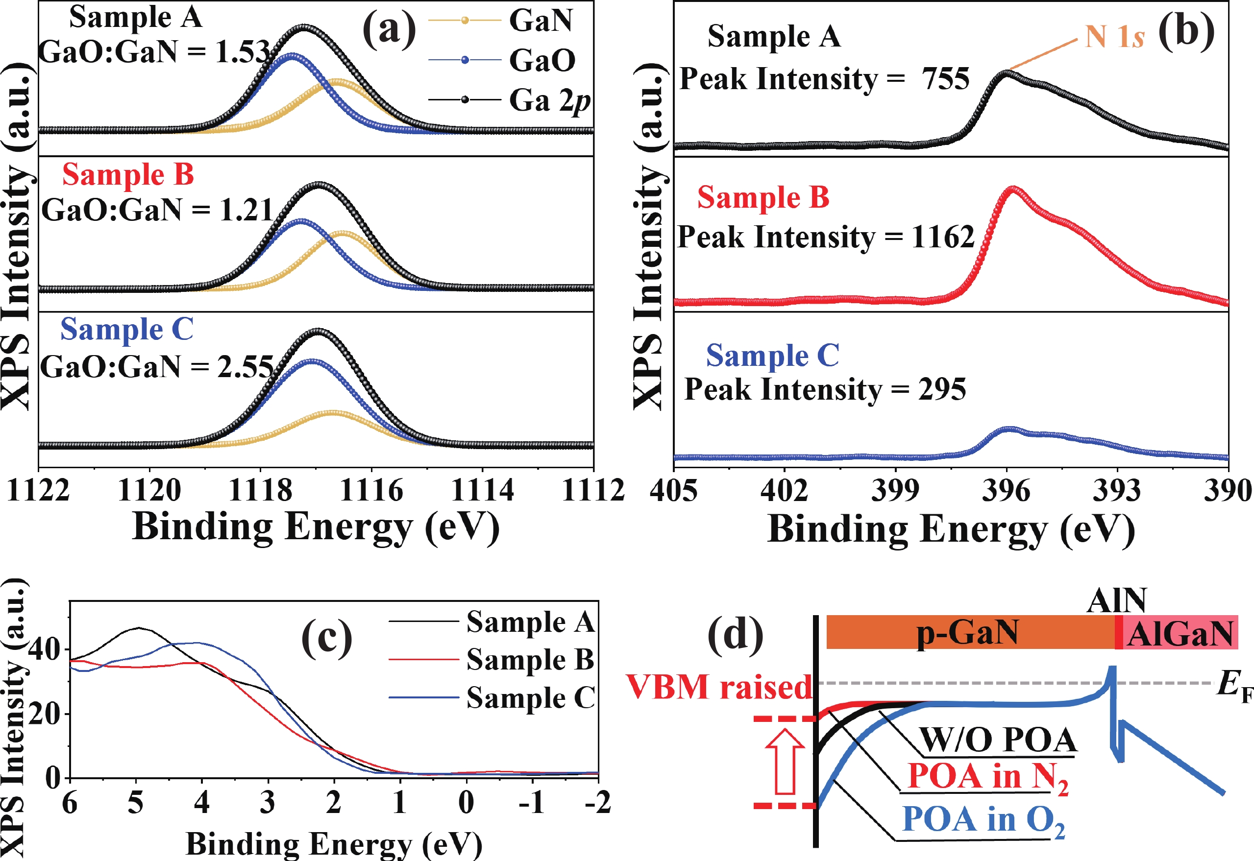
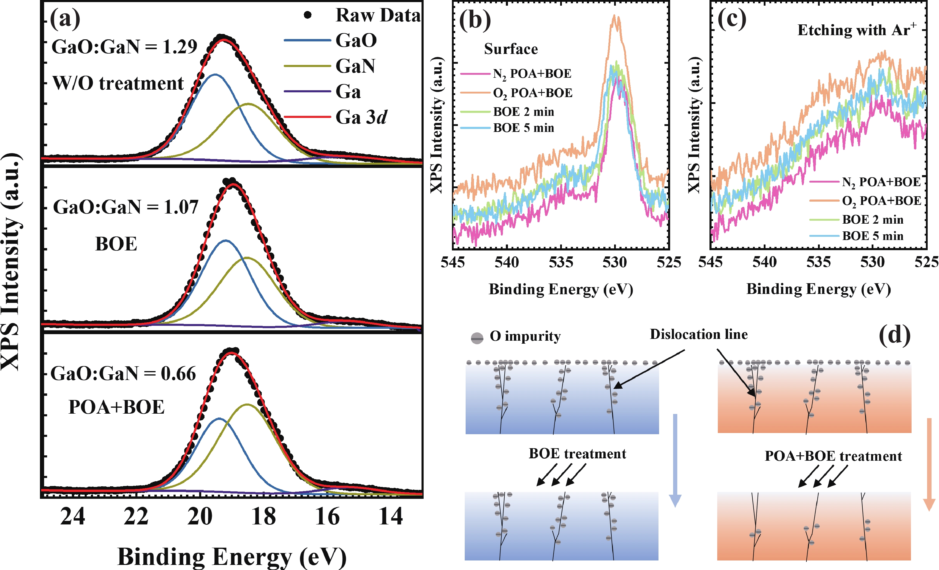
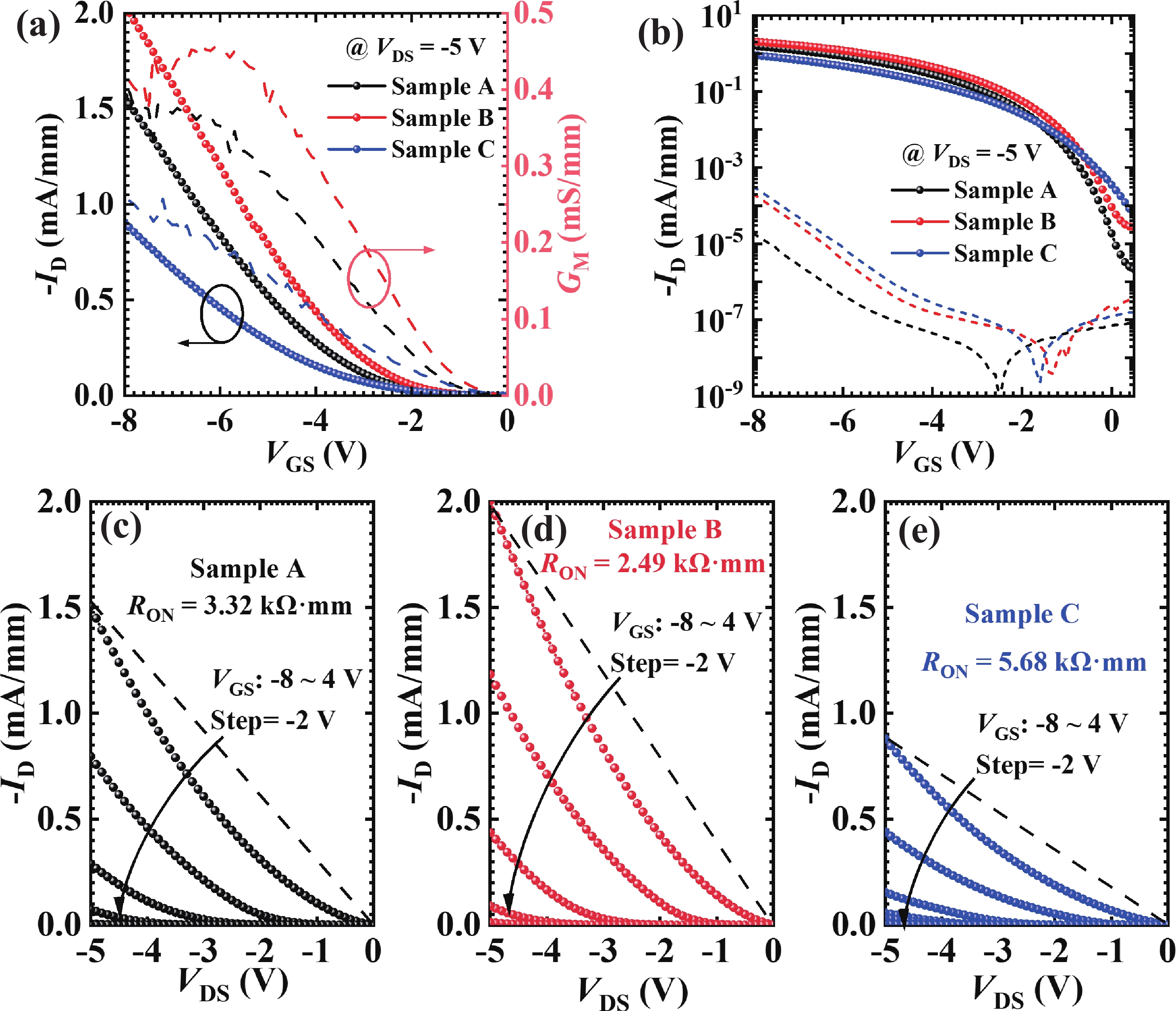
Table 1. 2DHG and Rsh measured by contact-Hall as well as Rsh extracted by TLM at 10 V of the three samples.
| Sample | 2DHG (1013 cm−2) |
Rsh (kΩ/□) | Rsh extracted by TLM (kΩ/□) |
| A | 3.94 | 24 | 32.9 |
| B | 4.53 | 21.5 | 28.6 |
| C | 3.22 | 25.4 | 33.4 |
 DownLoad: CSV
| [1] |
Tao H C, Xu S R, Zhang J C, et al. Improved crystal quality and enhanced optical performance of GaN enabled by ion implantation induced high-quality nucleation. Opt Express, 2023, 31, 20850 doi: 10.1364/OE.492088
|
| [2] |
Peng R S, Xu S R, Fan X M, et al. Application of nano-patterned InGaN fabricated by self-assembled Ni nano-masks in green InGaN/GaN multiple quantum wells. J Semicond, 2023, 44, 042801 doi: 10.1088/1674-4926/44/4/042801
|
| [3] |
Zhang T, Zhang J C, Zhou H, et al. A > 3 kV/2.94 mΩ·cm2 and low leakage current with low turn-on voltage lateral GaN Schottky barrier diode on silicon substrate with anode engineering technique. IEEE Electron Device Lett, 2019, 40, 1583 doi: 10.1109/LED.2019.2933314
|
| [4] |
Smorchkova I P, Elsass C R, Ibbetson J P, et al. Polarization-induced charge and electron mobility in AlGaN/GaN heterostructures grown by plasma-assisted molecular-beam epitaxy. J Appl Phys, 1999, 86, 4520 doi: 10.1063/1.371396
|
| [5] |
Cai Y, Zhou Y G, Chen K J, et al. High-performance enhancement-mode AlGaN/GaN HEMTs using fluoride-based plasma treatment. IEEE Electron Device Lett, 2005, 26, 435 doi: 10.1109/LED.2005.851122
|
| [6] |
Tang Z K, Jiang Q M, Lu Y Y, et al. 600-V normally off SiNx/AlGaN/GaN MIS-HEMT with large gate swing and low current collapse. IEEE Electron Device Lett, 2013, 34, 1373 doi: 10.1109/LED.2013.2279846
|
| [7] |
Zheng Z Y, Zhang L, Song W J, et al. Gallium nitride-based complementary logic integrated circuits. Nat Electron, 2021, 4, 595 doi: 10.1038/s41928-021-00611-y
|
| [8] |
Du H H, Liu Z H, Hao L, et al. High-performance E-mode p-channel GaN FinFET on silicon substrate with high ION/IOFF and high threshold voltage. IEEE Electron Device Lett, 2022, 43, 705 doi: 10.1109/LED.2022.3155152
|
| [9] |
Chowdhury N, Lemettinen J, Xie Q Y, et al. P-channel GaN transistor based on p-GaN/AlGaN/GaN on Si. IEEE Electron Device Lett, 2019, 40, 1036 doi: 10.1109/LED.2019.2916253
|
| [10] |
Yang C, Fu H Q, Peri P, et al. Enhancement-mode gate-recess-free GaN-based p-channel heterojunction field-effect transistor with ultra-low subthreshold swing. IEEE Electron Device Lett, 2021, 42, 1128 doi: 10.1109/LED.2021.3092040
|
| [11] |
Chowdhury N, Xie Q Y, Yuan M Y, et al. First demonstration of a self-aligned GaN p-FET. 2019 IEEE International Electron Devices Meeting (IEDM), 2019, 4.6. 1
|
| [12] |
Chowdhury N, Xie Q Y, Niroula J, et al. Field-induced acceptor ionization in enhancement-mode GaN p-MOSFETs. 2020 IEEE International Electron Devices Meeting (IEDM), 2020, 5.5. 12
|
| [13] |
Chowdhury N, Xie Q Y, Palacios T. Self-aligned E-mode GaN p-channel FinFET with ION > 100 mA/mm and ION/IOFF > 107. IEEE Electron Device Lett, 2022, 43, 358 doi: 10.1109/LED.2022.3140281
|
| [14] |
Nomoto K, Chaudhuri R, Bader S J, et al. GaN/AlN p-channel HFETs with Imax >420 mA/mm and ~20 GHz fT/fMAX. 2020 IEEE International Electron Devices Meeting (IEDM), 2020, 8.3. 1
|
| [15] |
Raj A, Krishna A, Hatui N, et al. GaN/AlGaN superlattice based E-mode p-channel MES-FinFET with regrown contacts and >50 mA/mm on-current. 2021 IEEE International Electron Devices Meeting (IEDM), 2021, 5.4. 1
|
| [16] |
Raj A, Krishna A, Romanczyk B, et al. GaN/AlGaN superlattice based E-mode hole channel FinFET with Schottky gate. IEEE Electron Device Lett, 2023, 44, 9 doi: 10.1109/LED.2022.3223331
|
| [17] |
Chowdhury N, Xie Q Y, Yuan M Y, et al. Regrowth-free GaN-based complementary logic on a Si substrate. IEEE Electron Device Lett, 2020, 41, 820 doi: 10.1109/LED.2020.2987003
|
| [18] |
Bader S J, Chaudhuri R, Nomoto K, et al. Gate-recessed E-mode p-channel HFET with high on-current based on GaN/AlN 2D hole gas. IEEE Electron Device Lett, 2018, 39, 1848 doi: 10.1109/LED.2018.2874190
|
| [19] |
Götz W, Johnson N M, Walker J, et al. Activation of acceptors in Mg-doped GaN grown by metalorganic chemical vapor deposition. Appl Phys Lett, 1996, 68, 667 doi: 10.1063/1.116503
|
| [20] |
Zhang G Y, Tong Y Z, Yang Z J, et al. Relationship of background carrier concentration and defects in GaN grown by metalorganic vapor phase epitaxy. Appl Phys Lett, 1997, 71, 3376 doi: 10.1063/1.120341
|
| [21] |
Cao X A, Pearton S J, Zhang A P, et al. Electrical effects of plasma damage in p-GaN. Appl Phys Lett, 1999, 75, 2569 doi: 10.1063/1.125080
|
| [22] |
Foster G M, Koehler A, Ebrish M, et al. Recovery from plasma etching-induced nitrogen vacancies in p-type gallium nitride using UV/O3 treatments. Appl Phys Lett, 2020, 117, 082103 doi: 10.1063/5.0021153
|
| [23] |
Bader S J, Chaudhuri R, Hickman A, et al. GaN/AlN Schottky-gate p-channel HFETs with InGaN contacts and 100 mA/mm on-current. 2019 IEEE International Electron Devices Meeting (IEDM), 2019, 4.5. 1
|
| [24] |
Lu S, Deki M, Wang J, et al. Ohmic contact on low-doping-density p-type GaN with nitrogen-annealed Mg. Appl Phys Lett, 2021, 119, 242104 doi: 10.1063/5.0076764
|
| [25] |
Wang J, Lu S, Cai W T, et al. Ohmic contact to p-type GaN enabled by post-growth diffusion of magnesium. IEEE Electron Device Lett, 2022, 43, 150 doi: 10.1109/LED.2021.3131057
|
| [26] |
Tang C Y, Lu H H, Qiao Z P, et al. Ohmic contact with a contact resistivity of 12 Ω·mm on p-GaN/AlGaN/GaN. IEEE Electron Device Lett, 2022, 43, 1412 doi: 10.1109/LED.2022.3193004
|
| [27] |
Su H K, Zhang T, Xu S R, et al. Mechanism of low Ohmic contact resistance to p-type GaN by suppressed edge dislocations. Appl Phys Lett, 2022, 120, 222101 doi: 10.1063/5.0090693
|
| [28] |
Wenzel R, Fischer G G, Schmid-Fetzer R. Ohmic contacts on p-GaN (Part I). Mater Sci Semicond Process, 2001, 4, 357 doi: 10.1016/S1369-8001(00)00177-3
|
| [29] |
Kalaitzakis F G, Pelekanos N T, Prystawko P, et al. Low resistance as-deposited Cr/Au contacts on p-type GaN. Appl Phys Lett, 2007, 91, 261103 doi: 10.1063/1.2828044
|
| [30] |
Pan S, Lu Y M, Liang Z B, et al. Optimization of annealing conditions for Ag/p-GaN ohmic contacts. Appl Phys A Mater Sci Process, 2021, 127, 870 doi: 10.1007/s00339-021-05022-6
|
| [31] |
Wahid S, Chowdhury N, Alam M K, et al. Barrier heights and Fermi level pinning in metal contacts on p-type GaN. Appl Phys Lett, 2020, 116, 213506 doi: 10.1063/5.0010699
|
| [32] |
Kim J K, Lee J L, Lee J W, et al. Low resistance Pd/Au ohmic contacts to p-type GaN using surface treatment. Appl Phys Lett, 1998, 73, 2953 doi: 10.1063/1.122641
|
| [33] |
Lee J L, Kim J K, Lee J W, et al. Effect of surface treatment by KOH solution on ohmic contact formation of p-type GaN. Solid State Electron, 1999, 43, 435 doi: 10.1016/S0038-1101(98)00265-2
|
| [34] |
Mori T, Kozawa T, Ohwaki T, et al. Schottky barriers and contact resistances on p-type GaN. Appl Phys Lett, 1996, 69, 3537 doi: 10.1063/1.117237
|
| [35] |
Pankove J I, Torvik J T, Qiu C H, et al. Molecular doping of gallium nitride. Appl Phys Lett, 1999, 74, 416 doi: 10.1063/1.123046
|
| [36] |
Wright A F. Substitutional and interstitial oxygen in wurtzite GaN. J Appl Phys, 2005, 98, 103531 doi: 10.1063/1.2137446
|
| [37] |
Arslan I, Browning N D. Role of oxygen at screw dislocations in GaN. Phys Rev Lett, 2003, 91, 165501 doi: 10.1103/PhysRevLett.91.165501
|
| [38] |
Zywietz T K, Neugebauer J, Scheffler M. The adsorption of oxygen at GaN surfaces. Appl Phys Lett, 1999, 74, 1695 doi: 10.1063/1.123658
|
| [39] |
Pearton S J, Cho H, LaRoche J R, et al. Oxygen diffusion into SiO2-capped GaN during annealing. Appl Phys Lett, 1999, 75, 2939 doi: 10.1063/1.125194
|
| [40] |
Huang B R, Chou C H, Ke W C, et al. Effects of hydrogen treatment on ohmic contacts to p-type GaN films. Appl Surf Sci, 2011, 257, 7490 doi: 10.1016/j.apsusc.2011.03.061
|
| [41] |
Reuters B, Hahn H, Pooth A, et al. Fabrication of p-channel heterostructure field effect transistors with polarization-induced two-dimensional hole gases at metal-polar GaN/AlInGaN interfaces. J Phys D Appl Phys, 2014, 47, 175103 doi: 10.1088/0022-3727/47/17/175103
|


Article views: 1616 Times PDF downloads: 155 Times Cited by: 0 Times
Received: 10 May 2024 Revised: 10 July 2024 Online: Accepted Manuscript: 26 August 2024Uncorrected proof: 27 August 2024Published: 15 November 2024
| Citation: |
Huake Su, Tao Zhang, Shengrui Xu, Hongchang Tao, Yibo Wang, Yuan Gao, Yue Hao, Jincheng Zhang. Investigation of performance-enhanced GaN-based E-mode p-channel MOSFET with pre-ohmic-annealing treatment[J]. Journal of Semiconductors, 2024, 45(11): 112501. doi: 10.1088/1674-4926/24050015
****
H K Su, T Zhang, S R Xu, H C Tao, Y B Wang, Y Gao, Y Hao, and J C Zhang, Investigation of performance-enhanced GaN-based E-mode p-channel MOSFET with pre-ohmic-annealing treatment[J]. J. Semicond., 2024, 45(11), 112501 doi: 10.1088/1674-4926/24050015

|
 Huake Su received the B.Eng. degree from Xidian University in 2019. He is currently pursuing the Ph.D. degree with the School of Microelectronics, Xidian University. His research interest focuses on GaN-based electronic devices
 Tao Zhang received the Ph.D. degree from Xidian University in 2020 under the supervision of Prof. Jincheng Zhang. Currently, he is an associate professor at Xidian University. His research interest focuses on wide-bandgap semiconductors and electronic devices
 Shengrui Xu received the B.S. and Ph.D. degrees from Xidian University, Xi’an, China, in 2005 and 2010, respectively. He is currently a Professor with the School of Microelectronics, Xidian University. His current research interests include GaN-based optoelectronic devices and wide gap-band materials and devices
 Jincheng Zhang received the M.S. and Ph.D. degrees from Xidian University, Xi’an, China, in 2001 and 2004, respectively. He is currently a Professor with Xidian University. His current research interests include wide gap-band semiconductor GaN and diamond materials and devices
| [1] |
Tao H C, Xu S R, Zhang J C, et al. Improved crystal quality and enhanced optical performance of GaN enabled by ion implantation induced high-quality nucleation. Opt Express, 2023, 31, 20850 doi: 10.1364/OE.492088
|
| [2] |
Peng R S, Xu S R, Fan X M, et al. Application of nano-patterned InGaN fabricated by self-assembled Ni nano-masks in green InGaN/GaN multiple quantum wells. J Semicond, 2023, 44, 042801 doi: 10.1088/1674-4926/44/4/042801
|
| [3] |
Zhang T, Zhang J C, Zhou H, et al. A > 3 kV/2.94 mΩ·cm2 and low leakage current with low turn-on voltage lateral GaN Schottky barrier diode on silicon substrate with anode engineering technique. IEEE Electron Device Lett, 2019, 40, 1583 doi: 10.1109/LED.2019.2933314
|
| [4] |
Smorchkova I P, Elsass C R, Ibbetson J P, et al. Polarization-induced charge and electron mobility in AlGaN/GaN heterostructures grown by plasma-assisted molecular-beam epitaxy. J Appl Phys, 1999, 86, 4520 doi: 10.1063/1.371396
|
| [5] |
Cai Y, Zhou Y G, Chen K J, et al. High-performance enhancement-mode AlGaN/GaN HEMTs using fluoride-based plasma treatment. IEEE Electron Device Lett, 2005, 26, 435 doi: 10.1109/LED.2005.851122
|
| [6] |
Tang Z K, Jiang Q M, Lu Y Y, et al. 600-V normally off SiNx/AlGaN/GaN MIS-HEMT with large gate swing and low current collapse. IEEE Electron Device Lett, 2013, 34, 1373 doi: 10.1109/LED.2013.2279846
|
| [7] |
Zheng Z Y, Zhang L, Song W J, et al. Gallium nitride-based complementary logic integrated circuits. Nat Electron, 2021, 4, 595 doi: 10.1038/s41928-021-00611-y
|
| [8] |
Du H H, Liu Z H, Hao L, et al. High-performance E-mode p-channel GaN FinFET on silicon substrate with high ION/IOFF and high threshold voltage. IEEE Electron Device Lett, 2022, 43, 705 doi: 10.1109/LED.2022.3155152
|
| [9] |
Chowdhury N, Lemettinen J, Xie Q Y, et al. P-channel GaN transistor based on p-GaN/AlGaN/GaN on Si. IEEE Electron Device Lett, 2019, 40, 1036 doi: 10.1109/LED.2019.2916253
|
| [10] |
Yang C, Fu H Q, Peri P, et al. Enhancement-mode gate-recess-free GaN-based p-channel heterojunction field-effect transistor with ultra-low subthreshold swing. IEEE Electron Device Lett, 2021, 42, 1128 doi: 10.1109/LED.2021.3092040
|
| [11] |
Chowdhury N, Xie Q Y, Yuan M Y, et al. First demonstration of a self-aligned GaN p-FET. 2019 IEEE International Electron Devices Meeting (IEDM), 2019, 4.6. 1
|
| [12] |
Chowdhury N, Xie Q Y, Niroula J, et al. Field-induced acceptor ionization in enhancement-mode GaN p-MOSFETs. 2020 IEEE International Electron Devices Meeting (IEDM), 2020, 5.5. 12
|
| [13] |
Chowdhury N, Xie Q Y, Palacios T. Self-aligned E-mode GaN p-channel FinFET with ION > 100 mA/mm and ION/IOFF > 107. IEEE Electron Device Lett, 2022, 43, 358 doi: 10.1109/LED.2022.3140281
|
| [14] |
Nomoto K, Chaudhuri R, Bader S J, et al. GaN/AlN p-channel HFETs with Imax >420 mA/mm and ~20 GHz fT/fMAX. 2020 IEEE International Electron Devices Meeting (IEDM), 2020, 8.3. 1
|
| [15] |
Raj A, Krishna A, Hatui N, et al. GaN/AlGaN superlattice based E-mode p-channel MES-FinFET with regrown contacts and >50 mA/mm on-current. 2021 IEEE International Electron Devices Meeting (IEDM), 2021, 5.4. 1
|
| [16] |
Raj A, Krishna A, Romanczyk B, et al. GaN/AlGaN superlattice based E-mode hole channel FinFET with Schottky gate. IEEE Electron Device Lett, 2023, 44, 9 doi: 10.1109/LED.2022.3223331
|
| [17] |
Chowdhury N, Xie Q Y, Yuan M Y, et al. Regrowth-free GaN-based complementary logic on a Si substrate. IEEE Electron Device Lett, 2020, 41, 820 doi: 10.1109/LED.2020.2987003
|
| [18] |
Bader S J, Chaudhuri R, Nomoto K, et al. Gate-recessed E-mode p-channel HFET with high on-current based on GaN/AlN 2D hole gas. IEEE Electron Device Lett, 2018, 39, 1848 doi: 10.1109/LED.2018.2874190
|
| [19] |
Götz W, Johnson N M, Walker J, et al. Activation of acceptors in Mg-doped GaN grown by metalorganic chemical vapor deposition. Appl Phys Lett, 1996, 68, 667 doi: 10.1063/1.116503
|
| [20] |
Zhang G Y, Tong Y Z, Yang Z J, et al. Relationship of background carrier concentration and defects in GaN grown by metalorganic vapor phase epitaxy. Appl Phys Lett, 1997, 71, 3376 doi: 10.1063/1.120341
|
| [21] |
Cao X A, Pearton S J, Zhang A P, et al. Electrical effects of plasma damage in p-GaN. Appl Phys Lett, 1999, 75, 2569 doi: 10.1063/1.125080
|
| [22] |
Foster G M, Koehler A, Ebrish M, et al. Recovery from plasma etching-induced nitrogen vacancies in p-type gallium nitride using UV/O3 treatments. Appl Phys Lett, 2020, 117, 082103 doi: 10.1063/5.0021153
|
| [23] |
Bader S J, Chaudhuri R, Hickman A, et al. GaN/AlN Schottky-gate p-channel HFETs with InGaN contacts and 100 mA/mm on-current. 2019 IEEE International Electron Devices Meeting (IEDM), 2019, 4.5. 1
|
| [24] |
Lu S, Deki M, Wang J, et al. Ohmic contact on low-doping-density p-type GaN with nitrogen-annealed Mg. Appl Phys Lett, 2021, 119, 242104 doi: 10.1063/5.0076764
|
| [25] |
Wang J, Lu S, Cai W T, et al. Ohmic contact to p-type GaN enabled by post-growth diffusion of magnesium. IEEE Electron Device Lett, 2022, 43, 150 doi: 10.1109/LED.2021.3131057
|
| [26] |
Tang C Y, Lu H H, Qiao Z P, et al. Ohmic contact with a contact resistivity of 12 Ω·mm on p-GaN/AlGaN/GaN. IEEE Electron Device Lett, 2022, 43, 1412 doi: 10.1109/LED.2022.3193004
|
| [27] |
Su H K, Zhang T, Xu S R, et al. Mechanism of low Ohmic contact resistance to p-type GaN by suppressed edge dislocations. Appl Phys Lett, 2022, 120, 222101 doi: 10.1063/5.0090693
|
| [28] |
Wenzel R, Fischer G G, Schmid-Fetzer R. Ohmic contacts on p-GaN (Part I). Mater Sci Semicond Process, 2001, 4, 357 doi: 10.1016/S1369-8001(00)00177-3
|
| [29] |
Kalaitzakis F G, Pelekanos N T, Prystawko P, et al. Low resistance as-deposited Cr/Au contacts on p-type GaN. Appl Phys Lett, 2007, 91, 261103 doi: 10.1063/1.2828044
|
| [30] |
Pan S, Lu Y M, Liang Z B, et al. Optimization of annealing conditions for Ag/p-GaN ohmic contacts. Appl Phys A Mater Sci Process, 2021, 127, 870 doi: 10.1007/s00339-021-05022-6
|
| [31] |
Wahid S, Chowdhury N, Alam M K, et al. Barrier heights and Fermi level pinning in metal contacts on p-type GaN. Appl Phys Lett, 2020, 116, 213506 doi: 10.1063/5.0010699
|
| [32] |
Kim J K, Lee J L, Lee J W, et al. Low resistance Pd/Au ohmic contacts to p-type GaN using surface treatment. Appl Phys Lett, 1998, 73, 2953 doi: 10.1063/1.122641
|
| [33] |
Lee J L, Kim J K, Lee J W, et al. Effect of surface treatment by KOH solution on ohmic contact formation of p-type GaN. Solid State Electron, 1999, 43, 435 doi: 10.1016/S0038-1101(98)00265-2
|
| [34] |
Mori T, Kozawa T, Ohwaki T, et al. Schottky barriers and contact resistances on p-type GaN. Appl Phys Lett, 1996, 69, 3537 doi: 10.1063/1.117237
|
| [35] |
Pankove J I, Torvik J T, Qiu C H, et al. Molecular doping of gallium nitride. Appl Phys Lett, 1999, 74, 416 doi: 10.1063/1.123046
|
| [36] |
Wright A F. Substitutional and interstitial oxygen in wurtzite GaN. J Appl Phys, 2005, 98, 103531 doi: 10.1063/1.2137446
|
| [37] |
Arslan I, Browning N D. Role of oxygen at screw dislocations in GaN. Phys Rev Lett, 2003, 91, 165501 doi: 10.1103/PhysRevLett.91.165501
|
| [38] |
Zywietz T K, Neugebauer J, Scheffler M. The adsorption of oxygen at GaN surfaces. Appl Phys Lett, 1999, 74, 1695 doi: 10.1063/1.123658
|
| [39] |
Pearton S J, Cho H, LaRoche J R, et al. Oxygen diffusion into SiO2-capped GaN during annealing. Appl Phys Lett, 1999, 75, 2939 doi: 10.1063/1.125194
|
| [40] |
Huang B R, Chou C H, Ke W C, et al. Effects of hydrogen treatment on ohmic contacts to p-type GaN films. Appl Surf Sci, 2011, 257, 7490 doi: 10.1016/j.apsusc.2011.03.061
|
| [41] |
Reuters B, Hahn H, Pooth A, et al. Fabrication of p-channel heterostructure field effect transistors with polarization-induced two-dimensional hole gases at metal-polar GaN/AlInGaN interfaces. J Phys D Appl Phys, 2014, 47, 175103 doi: 10.1088/0022-3727/47/17/175103
|

 WeChat ID
Journal of Semiconductors © 2017 All Rights Reserved 京ICP备05085259号-2


