| Citation: |
Sergey M. Suturin, Polina A. Dvortsova, Alexander M. Korovin, Vladimir V. Fedorov, Evgeniya Yu. Lobanova, Nikolai S. Sokolov. Hard X-ray resonant reflectivity studies of ultrathin WS2 layers grown by pulsed laser deposition[J]. Journal of Semiconductors, 2025, 46(3): 032701. doi: 10.1088/1674-4926/24080040
****
S M Suturin, P A Dvortsova, A M Korovin, V V Fedorov, E Y Lobanova, and N S Sokolov, Hard X-ray resonant reflectivity studies of ultrathin WS2 layers grown by pulsed laser deposition[J]. J. Semicond., 2025, 46(3), 032701 doi: 10.1088/1674-4926/24080040
|
Hard X-ray resonant reflectivity studies of ultrathin WS2 layers grown by pulsed laser deposition
DOI: 10.1088/1674-4926/24080040
CSTR: 32376.14.1674-4926.24080040
More Information-
Abstract
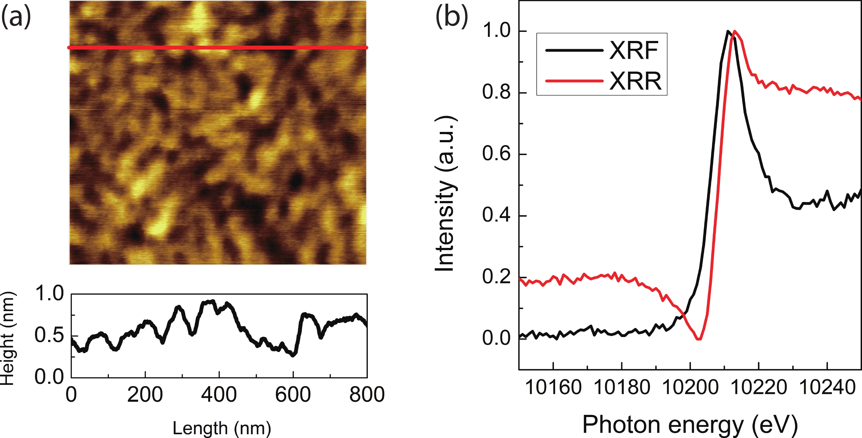
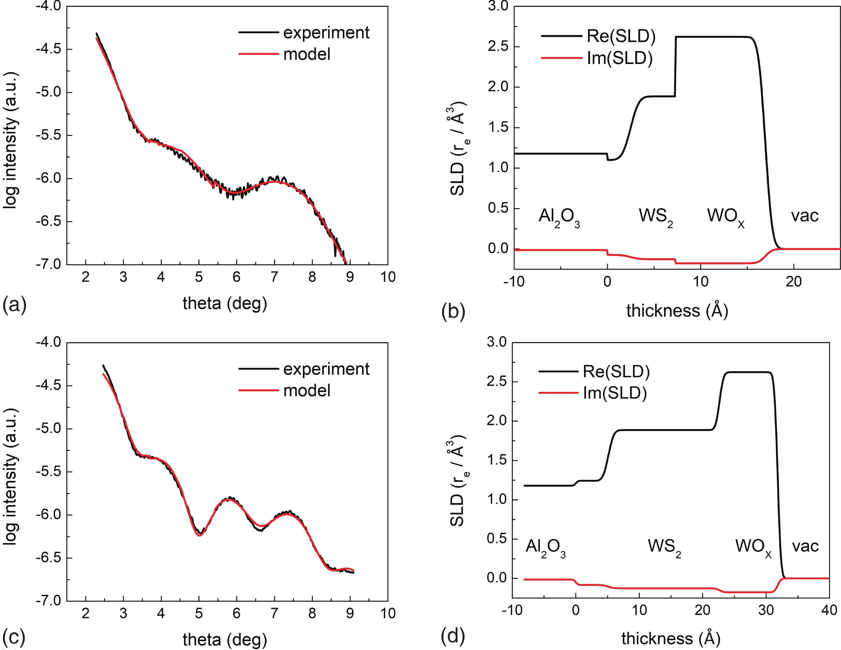
Synchrotron method of resonant X-ray reflectivity 2D mapping has been applied to study ultrathin epitaxial layers of WS2 grown by pulsed laser deposition on Al2O3(0001) substrates. The measurements were carried out across the L absorption edge of tungsten to perform depth-dependent element-selective analysis sensitive to potential chemical modification of the WS2 layer in ambient conditions. Despite the few monolayer thickness of the studied film, the experimentally measured maps of reflectance as a function of incident angle and photon energy turned out to be quite informative showing well-pronounced interference effects near W absorption edge at 10 210 eV. The synchrotron studies were complemented with conventional non-resonant reflectance measurements carried out in the laboratory at a fixed photon energy corresponding to Cu Kα emission. The reconstruction of the depth and energy dependent scattering length density within the studied multilayers was carried out using the OpenCL empowered fitting software utilizing spectral shaping algorithm which does not rely on the pre-measured reference absorption spectra. A thin WOx layer has been revealed at the surface of the WS2 layer pointing out to the effect of water assisted photo-oxidation reported in a number of works related to ultrathin layers of transition metal dichalcogenides. -
References
[1] Bolotsky A, Butler D, Dong C Y, et al. Two-dimensional materials in biosensing and healthcare: From in vitro diagnostics to optogenetics and beyond. ACS Nano, 2019, 13, 9781 doi: 10.1021/acsnano.9b03632[2] Wei T Y, Han Z C, Zhong X Y, et al. Two dimensional semiconducting materials for ultimately scaled transistors. iScience, 2022, 25, 105160 doi: 10.1016/j.isci.2022.105160[3] Novoselov K S, Mishchenko A, Carvalho A, et al. 2D materials and van der Waals heterostructures. Science, 2016, 353, eaac9439 doi: 10.1126/science.aac9439[4] Lasek K, Li J F, Kolekar S, et al. Synthesis and characterization of 2D transition metal dichalcogenides: Recent progress from a vacuum surface science perspective. Surf Sci Rep, 2021, 76, 100523 doi: 10.1016/j.surfrep.2021.100523[5] Liu L, Li T T, Ma L, et al. Uniform nucleation and epitaxy of bilayer molybdenum disulfide on sapphire. Nature, 2022, 605, 69 doi: 10.1038/s41586-022-04523-5[6] Wang J H, Xu X Z, Cheng T, et al. Dual-coupling-guided epitaxial growth of wafer-scale single-crystal WS2 monolayer on vicinal a-plane sapphire. Nat Nanotechnol, 2022, 17, 33 doi: 10.1038/s41565-021-01004-0[7] Yang P F, Wang D S, Zhao X X, et al. Epitaxial growth of inch-scale single-crystal transition metal dichalcogenides through the patching of unidirectionally orientated ribbons. Nat Commun, 2022, 13, 3238 doi: 10.1038/s41467-022-30900-9[8] Chubarov M, Choudhury T H, Hickey D R, et al. Wafer-scale epitaxial growth of unidirectional WS2 monolayers on sapphire. ACS Nano, 2021, 15, 2532 doi: 10.1021/acsnano.0c06750[9] Nakano M, Wang Y, Kashiwabara Y, et al. Layer-by-layer epitaxial growth of scalable WSe2 on sapphire by molecular beam epitaxy. Nano Lett, 2017, 17, 5595 doi: 10.1021/acs.nanolett.7b02420[10] Qiu H, Yu Z H, Zhao T G, et al. Two-dimensional materials for future information technology: Status and prospects. Sci China Inf Sci, 2024, 67, 160400 doi: 10.1007/s11432-024-4033-8[11] Zhao T G, Guo J X, Li T T, et al. Substrate engineering for wafer-scale two-dimensional material growth: Strategies, mechanisms, and perspectives. Chem Soc Rev, 2023, 52, 1650 doi: 10.1039/D2CS00657J[12] Molas M R, Nogajewski K, Potemski M, et al. Raman scattering excitation spectroscopy of monolayer WS2. Sci Rep, 2017, 7, 5036 doi: 10.1038/s41598-017-05367-0[13] Zeng H L, Liu G B, Dai J F, et al. Optical signature of symmetry variations and spin-valley coupling in atomically thin tungsten dichalcogenides. Sci Rep, 2013, 3, 1608 doi: 10.1038/srep01608[14] Rout C S, Joshi P D, Kashid R V, et al. Superior field emission properties of layered WS2-RGO nanocomposites. Sci Rep, 2013, 3, 3282 doi: 10.1038/srep03282[15] Sharma S, Bhagat S, Singh J, et al. Temperature dependent photoluminescence from WS2 nanostructures. J Mater Sci Mater Electron, 2018, 29, 20064 doi: 10.1007/s10854-018-0137-3[16] Abbas O A, Zeimpekis I, Wang H, et al. Solution-based synthesis of few-layer WS2 large area continuous films for electronic applications. Sci Rep, 2020, 10, 1696 doi: 10.1038/s41598-020-58694-0[17] Li G P, Wang Y L, Bi J T, et al. Partial oxidation strategy to synthesize WS2/WO3 heterostructure with enhanced adsorption performance for organic dyes: Synthesis, modelling, and mechanism. Nanomaterials, 2020, 10, 278 doi: 10.3390/nano10020278[18] Jha R, Guha P K. An effective liquid-phase exfoliation approach to fabricate tungsten disulfide into ultrathin two-dimensional semiconducting nanosheets. J Mater Sci, 2017, 52, 7256 doi: 10.1007/s10853-017-0962-4[19] Prouzet E, Heising J, Kanatzidis M G. Structure of restacked and pillared WS2: an X-ray absorption study. Chem Mater, 2003, 15, 412 doi: 10.1021/cm021186z[20] Hagopian N, He Y C, Rhodes D, et al. High resolution surface modification of WS2 via plasma oxidation and electron beam reduction. Microsc Microanal, 2024, 30, 5205 doi: 10.1093/mam/ozae044.602[21] Stone K H, Valvidares S M, Kortright J B. Kramers-Kronig constrained modeling of soft X-ray reflectivity spectra: Obtaining depth resolution of electronic and chemical structure. Phys Rev B, 2012, 86, 024102 doi: 10.1103/PhysRevB.86.024102[22] Pasquali L, Mahne N, Giglia A, et al. Analysis of resonant soft X-ray reflectivity of anisotropic layered materials. Surfaces, 2021, 4, 18 doi: 10.3390/surfaces4010004[23] Verna A, Capelli R, Pasquali L. Resonant soft X-ray reflectivity in the study of magnetic properties of low-dimensional systems. Magnetochemistry, 2021, 7, 136 doi: 10.3390/magnetochemistry7100136[24] Tonnerre J M, De Santis M, Grenier S, et al. Depth magnetization profile of a perpendicular exchange coupled system by soft-X-ray resonant magnetic reflectivity. Phys Rev Lett, 2008, 100, 157202 doi: 10.1103/PhysRevLett.100.157202[25] Suturin S M, Korovin A M, Gastev S V, et al. Tunable polymorphism of epitaxial iron oxides in the four-in-one ferroic-on-GaN system with magnetically ordered α-, γ-, ɛ–Fe2O3, and Fe3O4 layers. Phys Rev Materials, 2018, 2, 073403 doi: 10.1103/PhysRevMaterials.2.073403[26] Dvortsova P, Suturin S. A computational approach to predict and enhance the sensitivity of X-ray resonant magnetic reflectometry to the magnetic behavior of deeply buried interfaces. J Appl Crystallogr, 2024, 57, 151 doi: 10.1107/S1600576723011123[27] Dvortsova P A, Korovin A M M, Ukleev V, et al. Blind fit modeling of soft X-ray resonant reflectivity maps in nanoscale epitaxial iron oxide multilayers. J Appl Phys, 2024, 135, 055302 doi: 10.1063/5.0187303[28] Vanderlaan G. Studying spintronics materials with soft X-ray resonant scattering. Curr Opin Solid State Mater Sci, 2006, 10, 120 doi: 10.1016/j.cossms.2006.11.007[29] Hamann-Borrero J E, Macke S, Gray B, et al. Site-selective spectroscopy with depth resolution using resonant X-ray reflectometry. Sci Rep, 2017, 7, 13792 doi: 10.1038/s41598-017-12642-7[30] Lee K S, Kim S K, Kortright J B. Atomic-scale depth selectivity of soft X-ray resonant Kerr effect. Appl Phys Lett, 2003, 83, 3764 doi: 10.1063/1.1622123[31] Dvortsova P A, Suturin S M. Applicability of energy-theta mapping in resonant soft X-ray reflectometry to probe depth dependence of oxidation state and crystallographic environment in iron oxide multilayers. Thin Solid Films, 2024, 806, 140517 doi: 10.1016/j.tsf.2024.140517[32] Dvortsova P A, Korovin A M, Suturin S M. Intellectual fitting of hard X-ray resonant reflectance maps obtained for low-contrast oxide multilayers across L absorption edges of Eu and Gd. Mater Today Commun, 2024, 41, 110456 doi: 10.1016/j.mtcomm.2024.110456[33] Medvedev R V, Zameshin A A, Sturm J M, et al. W/B short period multilayer structures for soft x-rays. AIP Adv, 2020, 10, 045305 doi: 10.1063/1.5143397[34] Ren L L, Gao H F, Gao S T, et al. Determination of multilayer thicknesses of GaAs/AlAs superlattice by grazing incidence X-ray reflectivity. Int J Metrol Qual Eng, 2013, 4, 81 doi: 10.1051/ijmqe/2013040[35] Spiga D, Mirone A, Pareschi G, et al. Characterization of multilayer stack parameters from x-ray reflectivity data using the PPM program: measurements and comparison with TEM results. SPIE Proceedings Space Telescopes and Instrumentation II: Ultraviolet to Gamma Ray, 2006, 6266, 626616 doi: 10.1117/12.672895[36] Majhi A, Nayak M, Pradhan P C, et al. Soft X-ray reflection spectroscopy for nano-scaled layered structure materials. Sci Rep, 2018, 8, 15724 doi: 10.1038/s41598-018-34076-5[37] Parratt L G. Surface studies of solids by total reflection of X-rays. Phys Rev, 1954, 95, 359 doi: 10.1103/PhysRev.95.359[38] Henke B L, Gullikson E M, Davis J C. X-ray interactions: Photoabsorption, scattering, transmission, and reflection at E = 50-30, 000 eV, Z = 1-92. At Data Nucl Data Tables, 1993, 54, 181 doi: 10.1006/adnd.1993.1013[39] Björck M, Andersson G. GenX: An extensible X-ray reflectivity refinement program utilizing differential evolution. J Appl Crystallogr, 2007, 40, 1174 doi: 10.1107/S0021889807045086[40] Macke S, Radi A, Hamann-Borrero J E, et al. Element specific monolayer depth profiling. Adv Mater, 2014, 26, 6554 doi: 10.1002/adma.201402028[41] Vlachos D, Craven A J, McComb D W. Specimen charging in X-ray absorption spectroscopy: Correction of total electron yield data from stabilized zirconia in the energy range 250–915 eV. J Synchrotron Rad, 2005, 12, 224 doi: 10.1107/S0909049504030146[42] Trevorah R M, Chantler C T, Schalken M J. Solving self-absorption in fluorescence. IUCrJ, 2019, 6, 586 doi: 10.1107/S2052252519005128[43] Fürsich K, Zabolotnyy V B, Schierle E, et al. Theory-restricted resonant X-ray reflectometry of quantum materials. Phys Rev B, 2018, 97, 165126 doi: 10.1103/PhysRevB.97.165126[44] Georgioudakis M, Plevris V. A comparative study of differential evolution variants in constrained structural optimization. Front Built Environ, 2020, 6, 102 doi: 10.3389/fbuil.2020.00102[45] Kotsakidis J C, Zhang Q, Vazquez de Parga A L, et al. Oxidation of monolayer WS2 in ambient is a photoinduced process. Nano Lett, 2019, 19, 5205 doi: 10.1021/acs.nanolett.9b01599[46] Gao J, Li B C, Tan J W, et al. Aging of transition metal dichalcogenide monolayers. ACS Nano, 2016, 10, 2628 doi: 10.1021/acsnano.5b07677[47] Li J C, Ma Y Q, Zhang C, et al. Green electrosynthesis of 3, 3’-diamino-4, 4’-azofurazan energetic materials coupled with energy-efficient hydrogen production over Pt-based catalysts. Nat Commun, 2023, 14, 8146 doi: 10.1038/s41467-023-43698-x[48] Shi M Q, Jiang Z Z, Mei B B, et al. Tuning the hydrogen evolution performance of 2D tungsten disulfide by interfacial engineering. J Mater Chem A, 2021, 9, 7059 doi: 10.1039/D0TA10673A -
Proportional views


 Sergey M. Suturin received his doctoral degree from Ioffe Institute, St. Petersburg, Russia in 2002. He is currently a Leading Researcher with the Ioffe Institute. His research interests include fabrication and investigation of epitaxially grown heterostructures combining layers of functional materials. He has expertise in synchrotron-based techniques in application to the studies of structural, magnetic and electronic properties of the materials at nanoscale.
 DownLoad:


