


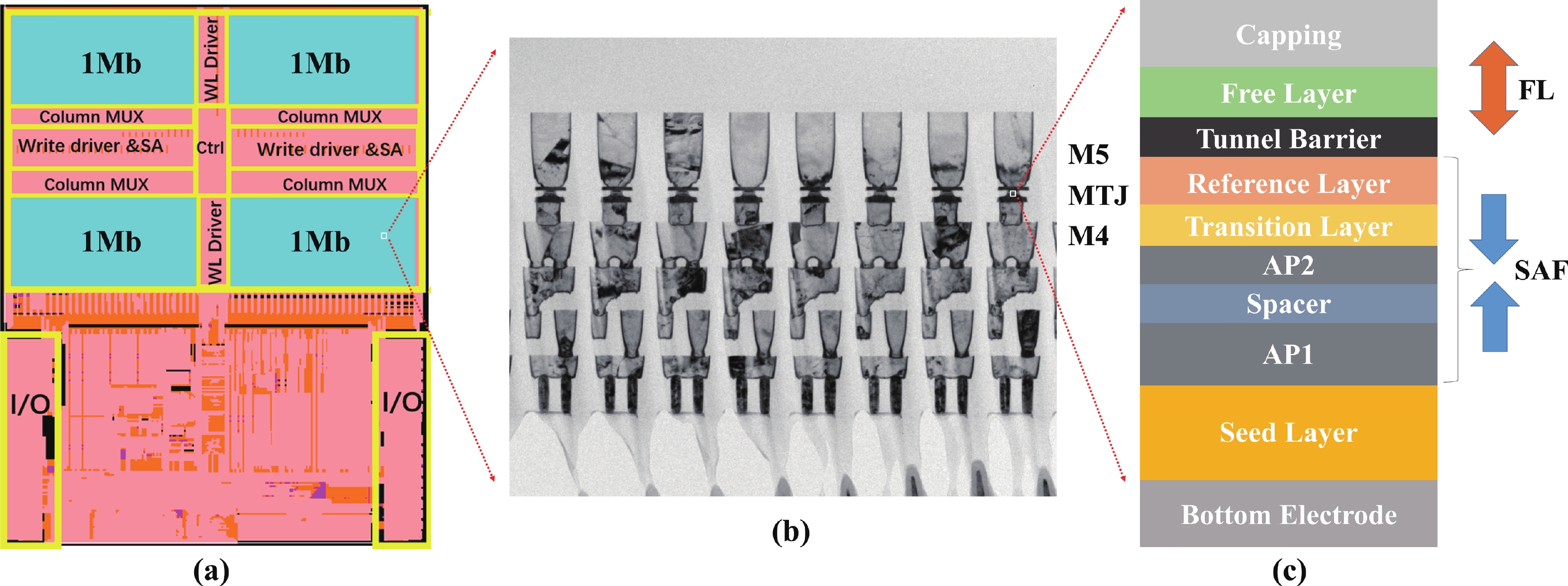
Fig. 1.
(Color online) (a) Layout of the 4 Mb eMRAM chip. (b) TEM cross section of the eMRAM array. (c) Storage element of magnetic tunnel junction (MTJ) stack layer illustration.
ARTICLES
Dinggui Zeng§, , Fantao Meng§, Ruofei Chen, Yang Gao, Yihui Sun, Junlu Gong, Yongzhao Peng, Qijun Guo, Zhixiao Deng, Weiming He, Baoyu Xiong, Jia Hou, Jichao Li, Wei Fang, Qiang Dai, Yaohua Wang and Shikun He
Corresponding author: Dinggui Zeng, zengdinggui@hikstor.com; Shikun He, he_shikun@hikstor.com
Abstract: Magnetic tunnel junction (MTJ) based spin transfer torque magnetic random access memory (STT-MRAM) has been gaining tremendous momentum in high performance microcontroller (MCU) applications. As eFlash-replacement type MRAM approaches mass production, there is an increasing demand for non-volatile RAM (nvRAM) technologies that offer fast write speed and high endurance. In this work, we demonstrate highly reliable 4 Mb nvRAM type MRAM suitable for industry and auto grade-1 applications. This nvRAM features retention over 10 years at 125 °C, endurance of 1 × 10¹² cycles with 20 ns write speed, making it ideal for applications requiring both high speed and broad temperature ranges. By employing innovative MTJ materials, process engineering, and a co-optimization of process and design, reliable read and write performance across the full temperature range between −40 to 125 °C, and array yield that meets sub-1 ppm error rate was significantly improved from 0 to above 95%, a concrete step toward applications.
Keywords: magnetic random access memory (MRAM), non-volatile RAM (nvRAM), magnetic tunnel junction (MTJ), sub-1 ppm array yield, reliability
| [1] |
Butler W H, Zhang X G, Schulthess T C, et al. Spin-dependent tunneling conductance of Fe| MgO|Fe sandwiches. Phys Rev B, 2001, 63, 054416 doi: 10.1103/PhysRevB.63.054416
|
| [2] |
Parkin S S P, Kaiser C, Panchula A, et al. Giant tunnelling magnetoresistance at room temperature with MgO (100) tunnel barriers. Nat Mater, 2004, 3, 862 doi: 10.1038/nmat1256
|
| [3] |
Ikeda S, Miura K, Yamamoto H, et al. A perpendicular-anisotropy CoFeB-MgO magnetic tunnel junction. Nat Mater, 2010, 9, 721 doi: 10.1038/nmat2804
|
| [4] |
Lee Y K, Song Y, Kim J, et al. Embedded STT-MRAM in 28-nm FDSOI logic process for industrial MCU/IoT application. 2018 IEEE Symposium on VLSI Technology, 2018, 181 doi: 10.1109/VLSIT.2018.8510623
|
| [5] |
Naik V B, Lee K, Yamane K, et al. Manufacturable 22nm FD-SOI embedded MRAM technology for industrial-grade MCU and IOT applications. 2019 IEEE International Electron Devices Meeting (IEDM), 2019, 2.3.1 doi: 10.1109/IEDM19573.2019.8993454
|
| [6] |
Shih Y C, Lee C F, Chang Y, et al. A reflow-capable, embedded 8Mb STT-MRAM macro with 9ns read access time in 16nm FinFET logic CMOS process. 2020 IEEE International Electron Devices Meeting (IEDM), 2020, 11.4.1 doi: 10.1109/IEDM13553.2020.9372115
|
| [7] |
Jung S, Lee H, Myung S, et al. A crossbar array of magnetoresistive memory devices for in-memory computing. Nature, 2022, 601, 211 doi: 10.1038/s41586-021-04196-6
|
| [8] |
Gallagher W J, Chien E, Chiang T W, et al. 22nm STT-MRAM for reflow and automotive uses with high yield, reliability, and magnetic immunity and with performance and shielding options. 2019 IEEE International Electron Devices Meeting (IEDM), 2019, 2.7.1 doi: 10.1109/IEDM19573.2019.8993469
|
| [9] |
Naik V B, Yamane K, Lee T Y, et al. JEDEC-qualified highly reliable 22nm FD-SOI embedded MRAM for low-power industrial-grade, and extended performance towards automotive-grade-1 applications. 2020 IEEE International Electron Devices Meeting (IEDM), 2020, 11.3.1 doi: 10.1109/IEDM13553.2020.9371935
|
| [10] |
Lee P H, Lee C F, Shih Y C, et al. A 16nm 32Mb embedded STT-MRAM with a 6ns read-access time, a 1M-cycle write endurance, 20-year retention at 150°C and MTJ-OTP solutions for magnetic immunity. 2023 IEEE International Solid-State Circuits Conference (ISSCC), 2023, 494 doi: 10.1109/ISSCC42615.2023.10067837
|
| [11] |
Ko S, Park J H, Bak J H, et al. Highly reliable and manufacturable MRAM embedded in 14nm FinFET node. 2023 IEEE Symposium on VLSI Technology and Circuits (VLSI Technology and Circuits), 2023, 1 doi: 10.23919/VLSITechnologyandCir57934.2023.10185248
|
| [12] |
Oh J, Park J, Suh K, et al. 14nm FinFET node embedded MRAM technology for automotive non-volatile RAM applications with endurance over 1E12-cycles. 2024 IEEE Symposium on VLSI Technology and Circuits (VLSI Technology and Circuits), 2024, 1 doi: 10.1109/VLSITechnologyandCir46783.2024.10631315
|
| [13] |
Lee T Y, Lee J M, Kim M K, et al. World-most energy-efficient MRAM technology for non-volatile RAM applications. 2022 International Electron Devices Meeting (IEDM), 2022, 10.7.1 doi: 10.1109/IEDM45625.2022.10019430
|
| [14] |
Amelichev V V, Vasilyev D V, Krikunov A I, et al. Synthetic antiferromagnetic structures in technology of spintronic devices. Nanobiotechnol Rep, 2021, 16, 155 doi: 10.1134/S2635167621020026
|
| [15] |
Yuasa S, Nagahama T, Fukushima A, et al. Giant room-temperature magnetoresistance in single-crystal Fe/MgO/Fe magnetic tunnel junctions. Nat Mater, 2004, 3, 868 doi: 10.1038/nmat1257
|
| [16] |
Wang Y, Chen Y H, Chih Y D, et al. High-speed embedded memory for AI and high-performance compute. 2023 International Electron Devices Meeting (IEDM), 2023, 1 doi: 10.1109/IEDM45741.2023.10413818
|
| [17] |
Dieny B, Aggarwal S, Naik V B, et al. Impact of external magnetic fields on STT-MRAM: An application note. IEEE Electron Devices Mag, 2024, 2, 52 doi: 10.1109/MED.2024.3442086
|
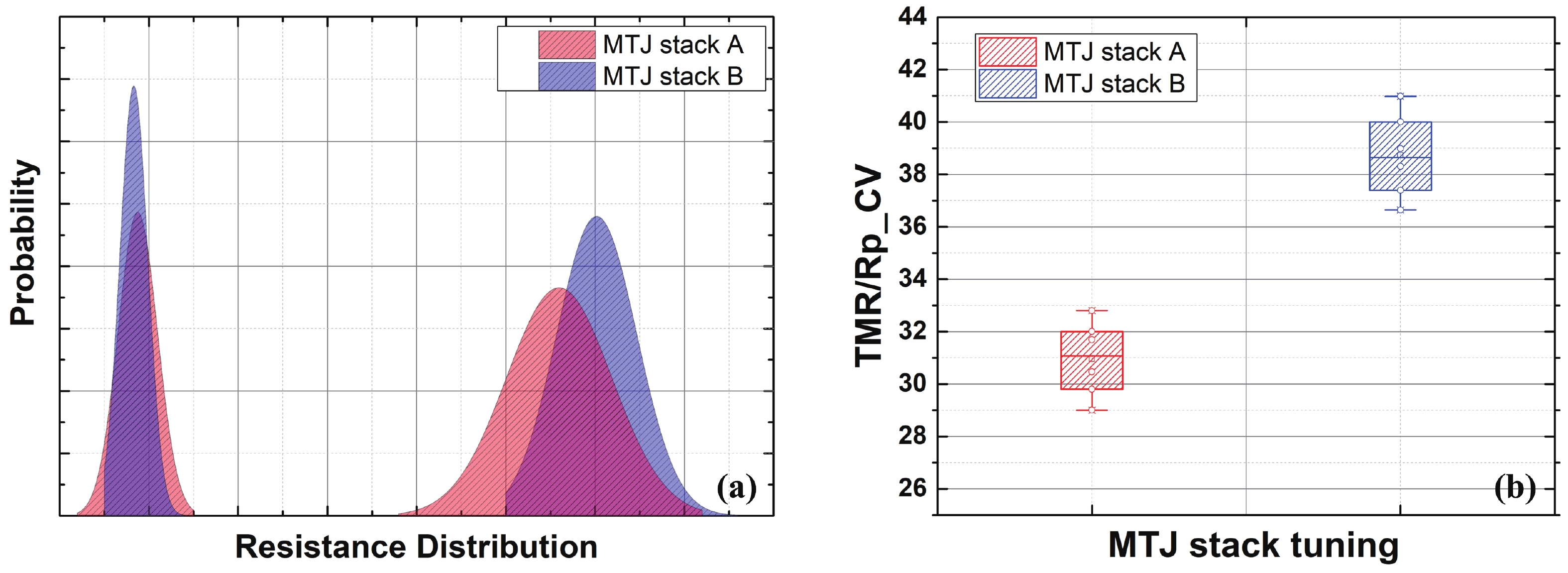
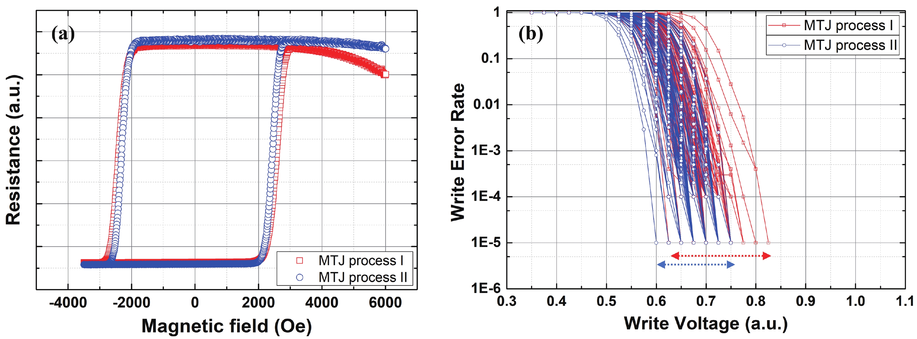
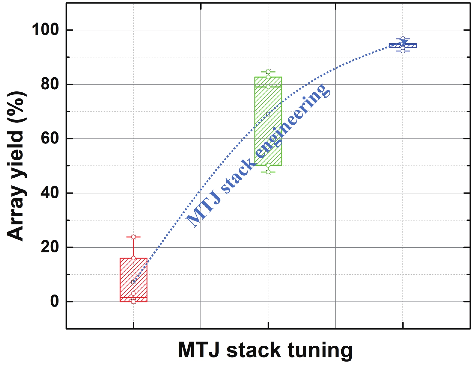
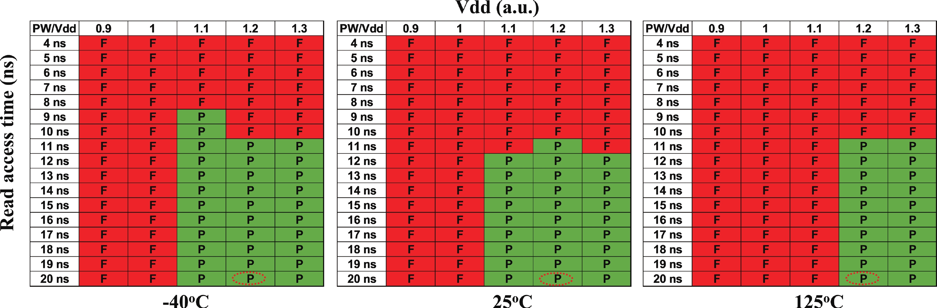
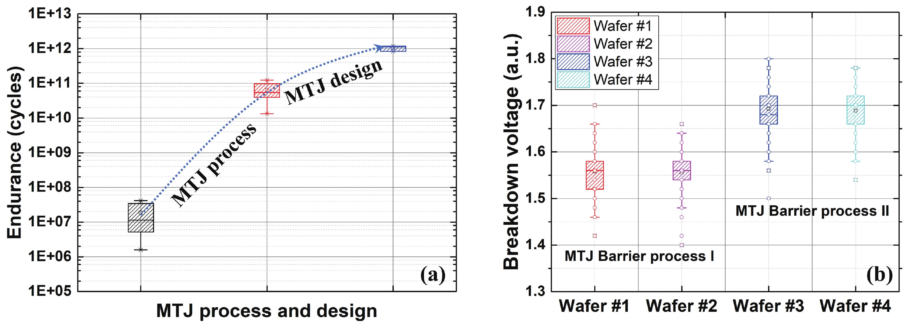
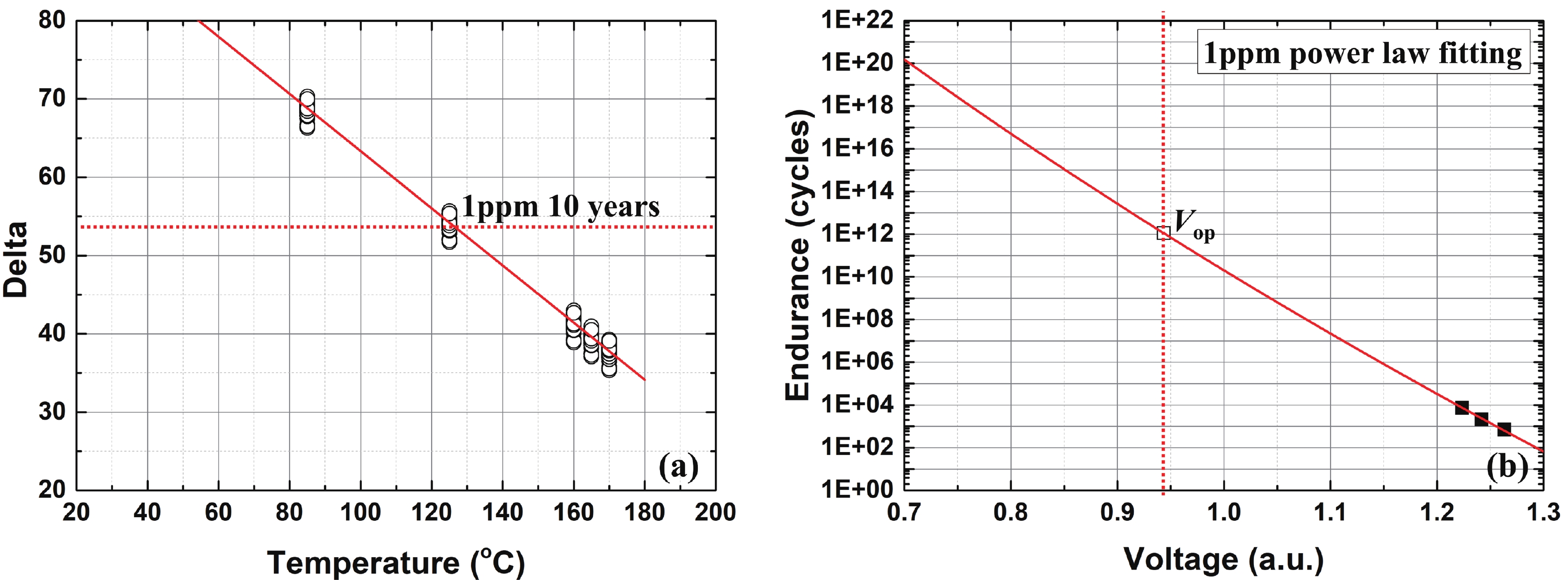
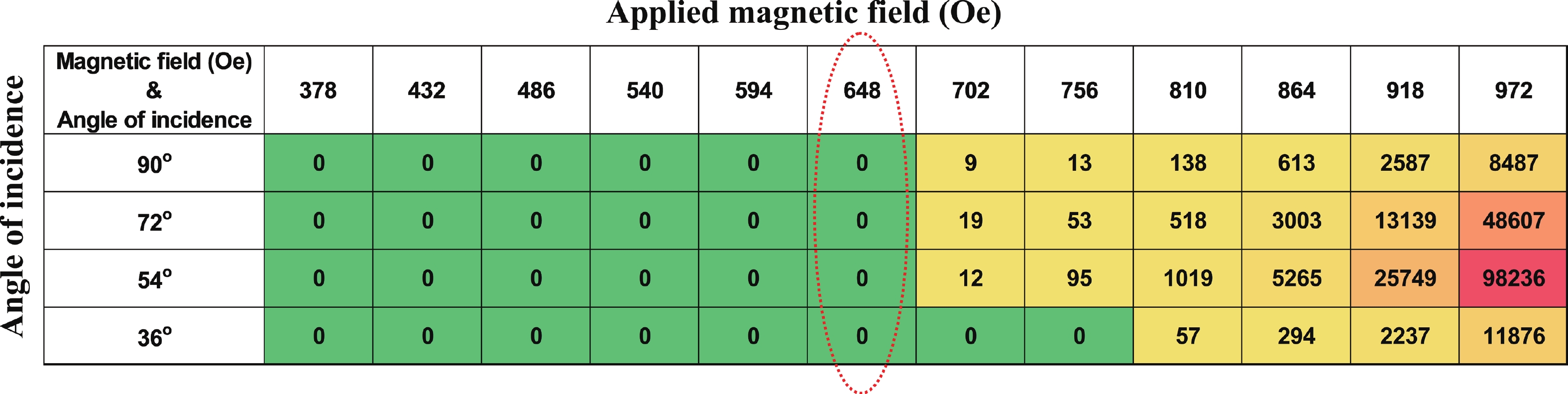
Table 1. MTJ performance comparisons with the previous literatures.
| Parameter | Ref. [12] | Ref. [13] | Ref. [16] | Ref. [8] | This work |
| Operating temperature (°C) | −40–125 | −40–85 | −40–125 | −40–150 | −40–125 |
| Memory density | 16 Mb | 16 Mb | Mb range | 32 Mb | 4 Mb |
| Read speed (ns) | 15 | 40 | NA | NA | 20 |
| Write speed (ns) | 100 | 160 | 20 | 50 | 20 |
| Endurance (cycle) | 1 × 10¹² | 1 × 10¹⁴ | 1 × 10¹² | 1 × 10⁶ | 1 × 10¹² |
| Retention | 10 years@150 °C | 10 years@89 °C | 10 sec@125 °C | 10 years@225 °C | 10 years@125 °C |
| Array yield@sub-1 ppm (w/o ECC & repair) (%) |
NA | NA | NA | 50–70 | 95 |
 DownLoad: CSV
| [1] |
Butler W H, Zhang X G, Schulthess T C, et al. Spin-dependent tunneling conductance of Fe| MgO|Fe sandwiches. Phys Rev B, 2001, 63, 054416 doi: 10.1103/PhysRevB.63.054416
|
| [2] |
Parkin S S P, Kaiser C, Panchula A, et al. Giant tunnelling magnetoresistance at room temperature with MgO (100) tunnel barriers. Nat Mater, 2004, 3, 862 doi: 10.1038/nmat1256
|
| [3] |
Ikeda S, Miura K, Yamamoto H, et al. A perpendicular-anisotropy CoFeB-MgO magnetic tunnel junction. Nat Mater, 2010, 9, 721 doi: 10.1038/nmat2804
|
| [4] |
Lee Y K, Song Y, Kim J, et al. Embedded STT-MRAM in 28-nm FDSOI logic process for industrial MCU/IoT application. 2018 IEEE Symposium on VLSI Technology, 2018, 181 doi: 10.1109/VLSIT.2018.8510623
|
| [5] |
Naik V B, Lee K, Yamane K, et al. Manufacturable 22nm FD-SOI embedded MRAM technology for industrial-grade MCU and IOT applications. 2019 IEEE International Electron Devices Meeting (IEDM), 2019, 2.3.1 doi: 10.1109/IEDM19573.2019.8993454
|
| [6] |
Shih Y C, Lee C F, Chang Y, et al. A reflow-capable, embedded 8Mb STT-MRAM macro with 9ns read access time in 16nm FinFET logic CMOS process. 2020 IEEE International Electron Devices Meeting (IEDM), 2020, 11.4.1 doi: 10.1109/IEDM13553.2020.9372115
|
| [7] |
Jung S, Lee H, Myung S, et al. A crossbar array of magnetoresistive memory devices for in-memory computing. Nature, 2022, 601, 211 doi: 10.1038/s41586-021-04196-6
|
| [8] |
Gallagher W J, Chien E, Chiang T W, et al. 22nm STT-MRAM for reflow and automotive uses with high yield, reliability, and magnetic immunity and with performance and shielding options. 2019 IEEE International Electron Devices Meeting (IEDM), 2019, 2.7.1 doi: 10.1109/IEDM19573.2019.8993469
|
| [9] |
Naik V B, Yamane K, Lee T Y, et al. JEDEC-qualified highly reliable 22nm FD-SOI embedded MRAM for low-power industrial-grade, and extended performance towards automotive-grade-1 applications. 2020 IEEE International Electron Devices Meeting (IEDM), 2020, 11.3.1 doi: 10.1109/IEDM13553.2020.9371935
|
| [10] |
Lee P H, Lee C F, Shih Y C, et al. A 16nm 32Mb embedded STT-MRAM with a 6ns read-access time, a 1M-cycle write endurance, 20-year retention at 150°C and MTJ-OTP solutions for magnetic immunity. 2023 IEEE International Solid-State Circuits Conference (ISSCC), 2023, 494 doi: 10.1109/ISSCC42615.2023.10067837
|
| [11] |
Ko S, Park J H, Bak J H, et al. Highly reliable and manufacturable MRAM embedded in 14nm FinFET node. 2023 IEEE Symposium on VLSI Technology and Circuits (VLSI Technology and Circuits), 2023, 1 doi: 10.23919/VLSITechnologyandCir57934.2023.10185248
|
| [12] |
Oh J, Park J, Suh K, et al. 14nm FinFET node embedded MRAM technology for automotive non-volatile RAM applications with endurance over 1E12-cycles. 2024 IEEE Symposium on VLSI Technology and Circuits (VLSI Technology and Circuits), 2024, 1 doi: 10.1109/VLSITechnologyandCir46783.2024.10631315
|
| [13] |
Lee T Y, Lee J M, Kim M K, et al. World-most energy-efficient MRAM technology for non-volatile RAM applications. 2022 International Electron Devices Meeting (IEDM), 2022, 10.7.1 doi: 10.1109/IEDM45625.2022.10019430
|
| [14] |
Amelichev V V, Vasilyev D V, Krikunov A I, et al. Synthetic antiferromagnetic structures in technology of spintronic devices. Nanobiotechnol Rep, 2021, 16, 155 doi: 10.1134/S2635167621020026
|
| [15] |
Yuasa S, Nagahama T, Fukushima A, et al. Giant room-temperature magnetoresistance in single-crystal Fe/MgO/Fe magnetic tunnel junctions. Nat Mater, 2004, 3, 868 doi: 10.1038/nmat1257
|
| [16] |
Wang Y, Chen Y H, Chih Y D, et al. High-speed embedded memory for AI and high-performance compute. 2023 International Electron Devices Meeting (IEDM), 2023, 1 doi: 10.1109/IEDM45741.2023.10413818
|
| [17] |
Dieny B, Aggarwal S, Naik V B, et al. Impact of external magnetic fields on STT-MRAM: An application note. IEEE Electron Devices Mag, 2024, 2, 52 doi: 10.1109/MED.2024.3442086
|


Article views: 3057 Times PDF downloads: 280 Times Cited by: 0 Times
Received: 19 September 2024 Revised: 08 November 2024 Online: Accepted Manuscript: 04 December 2024Uncorrected proof: 08 February 2025Published: 14 March 2025
| Citation: |
Dinggui Zeng, Fantao Meng, Ruofei Chen, Yang Gao, Yihui Sun, Junlu Gong, Yongzhao Peng, Qijun Guo, Zhixiao Deng, Weiming He, Baoyu Xiong, Jia Hou, Jichao Li, Wei Fang, Qiang Dai, Yaohua Wang, Shikun He. Achieving over 95% yield of sub-1 ppm BER with retention over 10 years at 125 °C and endurance of 1 × 10¹² cycles towards automotive non-volatile RAM applications[J]. Journal of Semiconductors, 2025, 46(3): 032301. doi: 10.1088/1674-4926/24090037
****
D G Zeng, F T Meng, R F Chen, Y Gao, Y H Sun, J L Gong, Y Z Peng, Q J Guo, Z X Deng, W M He, B Y Xiong, J Hou, J C Li, W Fang, Q Dai, Y H Wang, and S K He, Achieving over 95% yield of sub-1 ppm BER with retention over 10 years at 125 °C and endurance of 1 × 10¹² cycles towards automotive non-volatile RAM applications[J]. J. Semicond., 2025, 46(3), 032301 doi: 10.1088/1674-4926/24090037

|
 Dinggui Zeng got his BS in 2007 and PhD degree in 2012 at National University of Singapore. In Oct 2021, he joined Hikstor as MTJ thin film team leader. His R & D interests include magnetic storage, DRAM, emerging non-volatile memories especially MRAM
 Fantao Meng got his BS in 2005 and PhD degree in 2011 at Dalian University of Technology. Then he joined Intel as senior Process Engineer. In July 2016, he joined Hikstor as VP. His research interests include Emerging Non-Volatile Memory and semiconductor thin film process technology
 Shikun He got his BS in 2005 and PhD degree in 2012 at Institute of Physics Chinese Academy of Sciences. In 2016, he joined Hikstor as principle engineer and promoted to product R & D leader. His research interest focuses on spintronics materials, devices and systems
| [1] |
Butler W H, Zhang X G, Schulthess T C, et al. Spin-dependent tunneling conductance of Fe| MgO|Fe sandwiches. Phys Rev B, 2001, 63, 054416 doi: 10.1103/PhysRevB.63.054416
|
| [2] |
Parkin S S P, Kaiser C, Panchula A, et al. Giant tunnelling magnetoresistance at room temperature with MgO (100) tunnel barriers. Nat Mater, 2004, 3, 862 doi: 10.1038/nmat1256
|
| [3] |
Ikeda S, Miura K, Yamamoto H, et al. A perpendicular-anisotropy CoFeB-MgO magnetic tunnel junction. Nat Mater, 2010, 9, 721 doi: 10.1038/nmat2804
|
| [4] |
Lee Y K, Song Y, Kim J, et al. Embedded STT-MRAM in 28-nm FDSOI logic process for industrial MCU/IoT application. 2018 IEEE Symposium on VLSI Technology, 2018, 181 doi: 10.1109/VLSIT.2018.8510623
|
| [5] |
Naik V B, Lee K, Yamane K, et al. Manufacturable 22nm FD-SOI embedded MRAM technology for industrial-grade MCU and IOT applications. 2019 IEEE International Electron Devices Meeting (IEDM), 2019, 2.3.1 doi: 10.1109/IEDM19573.2019.8993454
|
| [6] |
Shih Y C, Lee C F, Chang Y, et al. A reflow-capable, embedded 8Mb STT-MRAM macro with 9ns read access time in 16nm FinFET logic CMOS process. 2020 IEEE International Electron Devices Meeting (IEDM), 2020, 11.4.1 doi: 10.1109/IEDM13553.2020.9372115
|
| [7] |
Jung S, Lee H, Myung S, et al. A crossbar array of magnetoresistive memory devices for in-memory computing. Nature, 2022, 601, 211 doi: 10.1038/s41586-021-04196-6
|
| [8] |
Gallagher W J, Chien E, Chiang T W, et al. 22nm STT-MRAM for reflow and automotive uses with high yield, reliability, and magnetic immunity and with performance and shielding options. 2019 IEEE International Electron Devices Meeting (IEDM), 2019, 2.7.1 doi: 10.1109/IEDM19573.2019.8993469
|
| [9] |
Naik V B, Yamane K, Lee T Y, et al. JEDEC-qualified highly reliable 22nm FD-SOI embedded MRAM for low-power industrial-grade, and extended performance towards automotive-grade-1 applications. 2020 IEEE International Electron Devices Meeting (IEDM), 2020, 11.3.1 doi: 10.1109/IEDM13553.2020.9371935
|
| [10] |
Lee P H, Lee C F, Shih Y C, et al. A 16nm 32Mb embedded STT-MRAM with a 6ns read-access time, a 1M-cycle write endurance, 20-year retention at 150°C and MTJ-OTP solutions for magnetic immunity. 2023 IEEE International Solid-State Circuits Conference (ISSCC), 2023, 494 doi: 10.1109/ISSCC42615.2023.10067837
|
| [11] |
Ko S, Park J H, Bak J H, et al. Highly reliable and manufacturable MRAM embedded in 14nm FinFET node. 2023 IEEE Symposium on VLSI Technology and Circuits (VLSI Technology and Circuits), 2023, 1 doi: 10.23919/VLSITechnologyandCir57934.2023.10185248
|
| [12] |
Oh J, Park J, Suh K, et al. 14nm FinFET node embedded MRAM technology for automotive non-volatile RAM applications with endurance over 1E12-cycles. 2024 IEEE Symposium on VLSI Technology and Circuits (VLSI Technology and Circuits), 2024, 1 doi: 10.1109/VLSITechnologyandCir46783.2024.10631315
|
| [13] |
Lee T Y, Lee J M, Kim M K, et al. World-most energy-efficient MRAM technology for non-volatile RAM applications. 2022 International Electron Devices Meeting (IEDM), 2022, 10.7.1 doi: 10.1109/IEDM45625.2022.10019430
|
| [14] |
Amelichev V V, Vasilyev D V, Krikunov A I, et al. Synthetic antiferromagnetic structures in technology of spintronic devices. Nanobiotechnol Rep, 2021, 16, 155 doi: 10.1134/S2635167621020026
|
| [15] |
Yuasa S, Nagahama T, Fukushima A, et al. Giant room-temperature magnetoresistance in single-crystal Fe/MgO/Fe magnetic tunnel junctions. Nat Mater, 2004, 3, 868 doi: 10.1038/nmat1257
|
| [16] |
Wang Y, Chen Y H, Chih Y D, et al. High-speed embedded memory for AI and high-performance compute. 2023 International Electron Devices Meeting (IEDM), 2023, 1 doi: 10.1109/IEDM45741.2023.10413818
|
| [17] |
Dieny B, Aggarwal S, Naik V B, et al. Impact of external magnetic fields on STT-MRAM: An application note. IEEE Electron Devices Mag, 2024, 2, 52 doi: 10.1109/MED.2024.3442086
|

 WeChat ID
Journal of Semiconductors © 2017 All Rights Reserved 京ICP备05085259号-2


