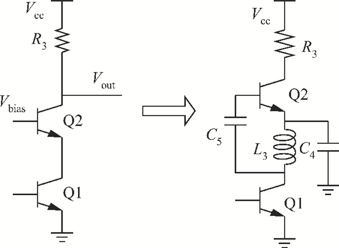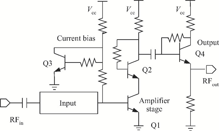
Fig. 1.
Structure of a dual-band LNA.
SEMICONDUCTOR INTEGRATED CIRCUITS
Zhiyi Lu, Hongyun Xie, Wenjuan Huo and Wanrong Zhang
Corresponding author: Lu Zhiyi, luzhiyi213@yahoo.com.cn
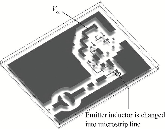
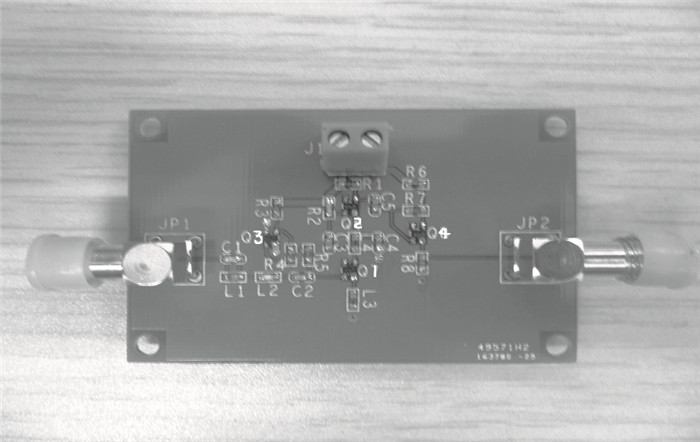
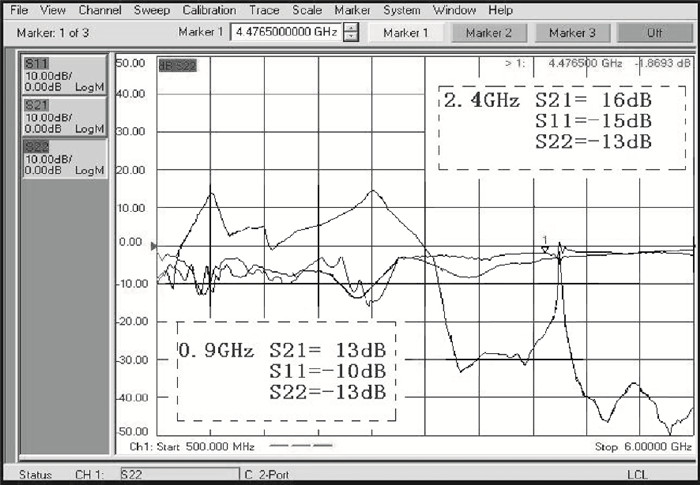
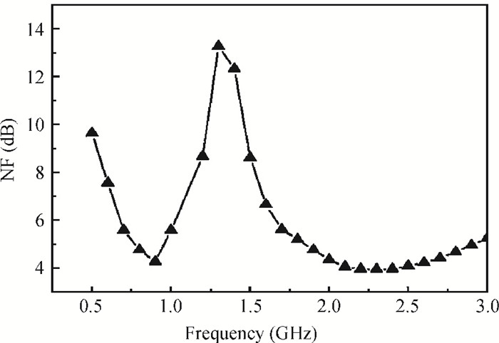
Abstract: This paper presents design and implementation of a dual-band LNA using a 0.35 μm SiGe HBT process for 0.9 GHz GSM and 2.4 GHz WLAN applications. PCB layout parasitic effects have a vital effect on circuit performance and are accounted for using electro-magnetic (EM) simulation. Design considerations of noise decoupling, input/output impedance matching, and current reuse are described in detail. At 0.9/2.4 GHz, gain and noise figure are 13/16 dB and 4.2/3.9 dB, respectively. Both S11 and S22 are below-10 dB. Power dissipation is 40 mW at 3.5 V supply.
Keywords: current reuse, dual-band, emitter inductor, EM simulation, SiGe HBT
| [1] |
Dao V K, Bui Q D, Park C S, et al. A multi-band 900 MHz/1.8 GHz/5.2 GHz LNA for reconfigurable radio. Radio Frequency Integrated Circuits Symposium, 2007, 1:69 http://ieeexplore.ieee.org/document/4266383/?arnumber=4266383&punumber%3D4266345
|
| [2] |
Amor M B, Douss S, Fakhfakh A, et al. Optimized design of a dual band low noise amplifier for the third generation of wireless system. SSD, 2005, 1:21 http://www.sciencedirect.com/science/article/pii/S2212017316304777
|
| [3] |
Wang R L, Chen S C, Huang C L. Single/multiband COMS low-noise amplifier using concentric switching inductors. Microw Opt Technol Lett, 2012, 54(2):309 doi: 10.1002/mop.v54.2
|
| [4] |
Datta S, Datta K, Dutta A. Fully concurrent dual-band LNA operating in 900 MHz/2.4 GHz bands for multi-standard wireless receiver with sub-2 dB noise figure. ICETET, 2010:731 http://ieeexplore.ieee.org/document/5698423/
|
| [5] |
Zhang Q Q, Liu Z F. Design of a concurrent dual-band LNA for GSM900 and GPS system. Microelectronics, 2011, 41(6):824
|
| [6] |
Wang S, Huang B Z. A high-gain CMOS LNA for 2.4/5.2 GHz WLAN applications. Progress in Electromagnetics Research C, 2011, 21:155 doi: 10.2528/PIERC11032705
|
| [7] |
Guo F, Li Z Q. The design of wideband CMOS VGA. Chinese Journal of Semiconductors, 2007, 28(12):1967 https://zh.scientific.net/AMR.1049-1050.682
|
| [8] |
Niknejad A M. Modeling of passive elements with ASITIC. IEEE MTTS Int Microw Symp Digest, 2002, 1(1):149 http://ieeexplore.ieee.org/document/1011581/
|
| [9] |
Xie H Y, Lu Z Y, Zhang W R. A dual-band SiGe HBT low noise amplifier. ICSICT, 2010, 1:568 http://ieeexplore.ieee.org/document/5667287/
|
| [10] |
Hao Mingli, Shi Yin. A 2.4 GHz power amplifier in 0.35μm SiGe BiCMOS. Journal of Semiconductors, 2010, 31(1):015004 doi: 10.1088/1674-4926/31/1/015004
|
| [11] |
Lin Y J, Hsu S H, Jin J D, et al. A 3.1-10.6 GHz ultra-wideband CMOS LNA with current reuse technique. IEEE Microw Wireless Compon Lett, 2007, 17(3):232 doi: 10.1109/LMWC.2006.890503
|
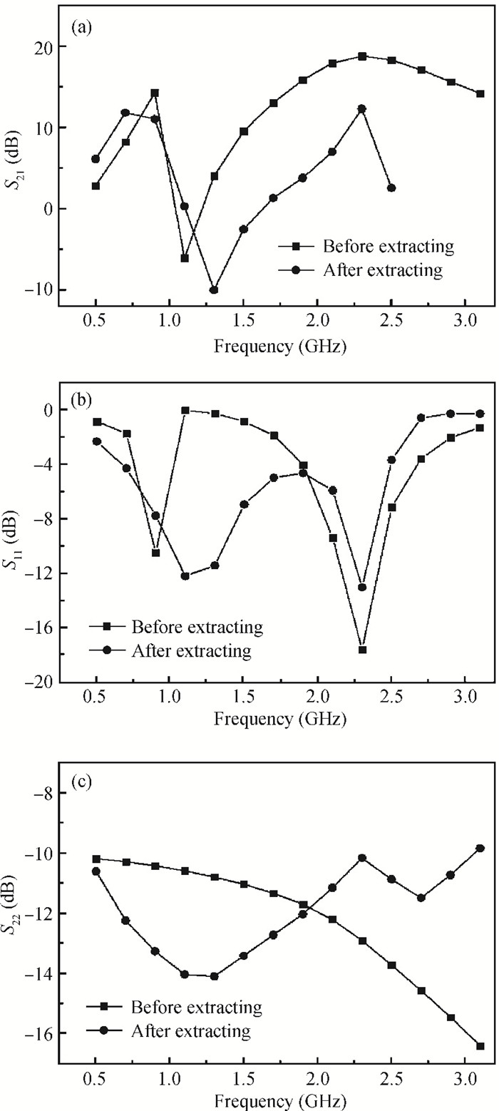
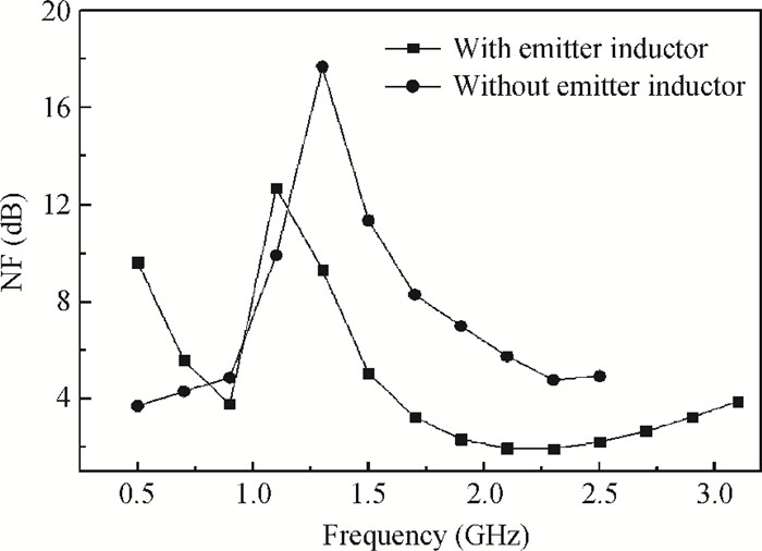
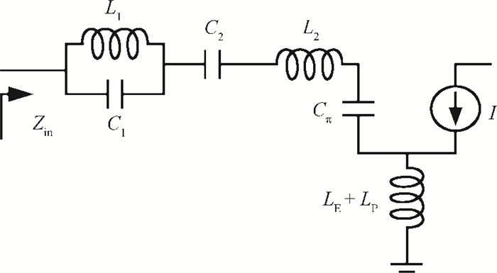
Table 1. Comparison of LNAs operating in similar bands.

|
| [1] |
Dao V K, Bui Q D, Park C S, et al. A multi-band 900 MHz/1.8 GHz/5.2 GHz LNA for reconfigurable radio. Radio Frequency Integrated Circuits Symposium, 2007, 1:69 http://ieeexplore.ieee.org/document/4266383/?arnumber=4266383&punumber%3D4266345
|
| [2] |
Amor M B, Douss S, Fakhfakh A, et al. Optimized design of a dual band low noise amplifier for the third generation of wireless system. SSD, 2005, 1:21 http://www.sciencedirect.com/science/article/pii/S2212017316304777
|
| [3] |
Wang R L, Chen S C, Huang C L. Single/multiband COMS low-noise amplifier using concentric switching inductors. Microw Opt Technol Lett, 2012, 54(2):309 doi: 10.1002/mop.v54.2
|
| [4] |
Datta S, Datta K, Dutta A. Fully concurrent dual-band LNA operating in 900 MHz/2.4 GHz bands for multi-standard wireless receiver with sub-2 dB noise figure. ICETET, 2010:731 http://ieeexplore.ieee.org/document/5698423/
|
| [5] |
Zhang Q Q, Liu Z F. Design of a concurrent dual-band LNA for GSM900 and GPS system. Microelectronics, 2011, 41(6):824
|
| [6] |
Wang S, Huang B Z. A high-gain CMOS LNA for 2.4/5.2 GHz WLAN applications. Progress in Electromagnetics Research C, 2011, 21:155 doi: 10.2528/PIERC11032705
|
| [7] |
Guo F, Li Z Q. The design of wideband CMOS VGA. Chinese Journal of Semiconductors, 2007, 28(12):1967 https://zh.scientific.net/AMR.1049-1050.682
|
| [8] |
Niknejad A M. Modeling of passive elements with ASITIC. IEEE MTTS Int Microw Symp Digest, 2002, 1(1):149 http://ieeexplore.ieee.org/document/1011581/
|
| [9] |
Xie H Y, Lu Z Y, Zhang W R. A dual-band SiGe HBT low noise amplifier. ICSICT, 2010, 1:568 http://ieeexplore.ieee.org/document/5667287/
|
| [10] |
Hao Mingli, Shi Yin. A 2.4 GHz power amplifier in 0.35μm SiGe BiCMOS. Journal of Semiconductors, 2010, 31(1):015004 doi: 10.1088/1674-4926/31/1/015004
|
| [11] |
Lin Y J, Hsu S H, Jin J D, et al. A 3.1-10.6 GHz ultra-wideband CMOS LNA with current reuse technique. IEEE Microw Wireless Compon Lett, 2007, 17(3):232 doi: 10.1109/LMWC.2006.890503
|


Article views: 3186 Times PDF downloads: 16 Times Cited by: 0 Times
Received: 16 May 2012 Revised: 08 September 2012 Online: Published: 01 February 2013
| Citation: |
Zhiyi Lu, Hongyun Xie, Wenjuan Huo, Wanrong Zhang. 0.9 GHz and 2.4 GHz dual-band SiGe HBT LNA[J]. Journal of Semiconductors, 2013, 34(2): 025002. doi: 10.1088/1674-4926/34/2/025002
****
Z Y Lu, H Y Xie, W J Huo, W R Zhang. 0.9 GHz and 2.4 GHz dual-band SiGe HBT LNA[J]. J. Semicond., 2013, 34(2): 025002. doi: 10.1088/1674-4926/34/2/025002.

|
| [1] |
Dao V K, Bui Q D, Park C S, et al. A multi-band 900 MHz/1.8 GHz/5.2 GHz LNA for reconfigurable radio. Radio Frequency Integrated Circuits Symposium, 2007, 1:69 http://ieeexplore.ieee.org/document/4266383/?arnumber=4266383&punumber%3D4266345
|
| [2] |
Amor M B, Douss S, Fakhfakh A, et al. Optimized design of a dual band low noise amplifier for the third generation of wireless system. SSD, 2005, 1:21 http://www.sciencedirect.com/science/article/pii/S2212017316304777
|
| [3] |
Wang R L, Chen S C, Huang C L. Single/multiband COMS low-noise amplifier using concentric switching inductors. Microw Opt Technol Lett, 2012, 54(2):309 doi: 10.1002/mop.v54.2
|
| [4] |
Datta S, Datta K, Dutta A. Fully concurrent dual-band LNA operating in 900 MHz/2.4 GHz bands for multi-standard wireless receiver with sub-2 dB noise figure. ICETET, 2010:731 http://ieeexplore.ieee.org/document/5698423/
|
| [5] |
Zhang Q Q, Liu Z F. Design of a concurrent dual-band LNA for GSM900 and GPS system. Microelectronics, 2011, 41(6):824
|
| [6] |
Wang S, Huang B Z. A high-gain CMOS LNA for 2.4/5.2 GHz WLAN applications. Progress in Electromagnetics Research C, 2011, 21:155 doi: 10.2528/PIERC11032705
|
| [7] |
Guo F, Li Z Q. The design of wideband CMOS VGA. Chinese Journal of Semiconductors, 2007, 28(12):1967 https://zh.scientific.net/AMR.1049-1050.682
|
| [8] |
Niknejad A M. Modeling of passive elements with ASITIC. IEEE MTTS Int Microw Symp Digest, 2002, 1(1):149 http://ieeexplore.ieee.org/document/1011581/
|
| [9] |
Xie H Y, Lu Z Y, Zhang W R. A dual-band SiGe HBT low noise amplifier. ICSICT, 2010, 1:568 http://ieeexplore.ieee.org/document/5667287/
|
| [10] |
Hao Mingli, Shi Yin. A 2.4 GHz power amplifier in 0.35μm SiGe BiCMOS. Journal of Semiconductors, 2010, 31(1):015004 doi: 10.1088/1674-4926/31/1/015004
|
| [11] |
Lin Y J, Hsu S H, Jin J D, et al. A 3.1-10.6 GHz ultra-wideband CMOS LNA with current reuse technique. IEEE Microw Wireless Compon Lett, 2007, 17(3):232 doi: 10.1109/LMWC.2006.890503
|

 WeChat ID
Journal of Semiconductors © 2017 All Rights Reserved 京ICP备05085259号-2

 DownLoad: