J. Semicond. > 2013, Volume 34 > Issue 2 > 025003

SEMICONDUCTOR INTEGRATED CIRCUITS

A clock generator for a high-speed high-resolution pipelined A/D converter

Lei Zhao, Yintang Yang, Zhangming Zhu and Lianxi Liu

+ Author Affiliations

 Corresponding author: Zhao Lei, Email:leizhao.ic@gmail.com

DOI: 10.1088/1674-4926/34/2/025003

PDF

Abstract: A clock generator circuit for a high-speed high-resolution pipelined A/D converter is presented. The circuit is realized by a delay locked loop (DLL), and a new differential structure is used to improve the precision of the charge pump. Meanwhile, a dynamic logic phase detector and a three transistor NAND logic circuit are proposed to reduce the output jitter by improving the steepness of the clock transition. The proposed circuit, designed by SMIC 0.18 μm 3.3 V CMOS technology, is used as a clock generator for a 14 bit 100 MS/s pipelined ADC. The simulation results have shown that the duty cycle ranged from 10% to 90% and can be adjusted. The average duty cycle error is less than 1%. The lock-time is only 13 clock cycles. The active area is 0.05 mm2 and power consumption is less than 15 mW.

Key words: duty cycle stabilizerclock jitterdynamic logicnon-overlap clock


[1]
Shin D, Kim C, Song J, et al. A 7 ps jitter 0.053 mm fast lock all-digital DLL with a wide range and high resolution DCC. IEEE J Solid-State Circuits, 2009, 44(9):2437 doi: 10.1109/JSSC.2009.2021447
[2]
Weng R M, Liu C Y, Lu Y C. A low jitter DLL-based pulse width control loop with duty cycle adjustment. IEEE Asia Pacific Conference on Circuits and Systems, 2008:418
[3]
Han S R, Liu S I. A 500 MHz-1.25 GHz fast-locking pulsewidth control loop with presentable duty cycle. IEEE J Solid-State Circuits, 2004, 39(3):463 doi: 10.1109/JSSC.2003.822781
[4]
Cheng K H, Su C W, Chang K F. A high linearity, fast-locking pulsewidth control loop with digitally programmable duty cycle correction for wide range operation. IEEE J Solid-State Circuits, 2008, 43(2):399 doi: 10.1109/JSSC.2007.914286
[5]
Lin T H, Chi C C, Chiu W H, et al. A synchronous 50% duty-cycle clock generator in 0.35μm CMOS. IEEE Trans Very Large Scale Integrated Circuits (VLSI) System, 2011, 19(4):585 doi: 10.1109/TVLSI.2009.2037910
[6]
Kao S K, You Y D. Pulse width control loop with low control voltage ripple. Proceedings of the International Multi Conference of Engineers and Computer Scientists, 2012, 2:23 http://www.chinabaike.com/FileUploadDir/autoelectronics/OtherFile/AUCOL_2008JUL24_POT_TA_32.pdf
[7]
Cheng K H, Su C W, Chang K F, et al. A high linearity and fast-locked pulse width control loop with digitally programmable output duty cycle for wide range operation. Proceedings of the 32th European Solid-State Circuits Conference, Montreux, Switzerland, 2006:178
[8]
Navidi M M, Abrishamifar A. A fast lock time pulsewidth control loop using second order passive loop filters. 19th Iranian Conference on Electrical Engineering (ICEE), 2011:1
[9]
Chandrakasan A, Bowhill W J, Fox F. Design of high-performance microprocessor circuit. New York:IEEE Press, 2001
[10]
Zhou X, Wang J, Pang S, et al. A clock management circuit in high-speed pipeline ADC. Electronics & Packaging, 2007, 7(3):20 https://arxiv.org/pdf/0808.0374
[11]
Chen Y G, Tsao H W, Hwang C S. A fast-locking all-digital Deskew buffer with duty-cycle correction. IEEE Trans Very Large Scale Integrated Circuits (VLSI) System, 2012, 99:1 doi: 10.1007%2Fs10470-017-1005-4.pdf
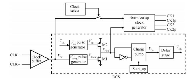
Fig. 1.  Proposed clock generator.

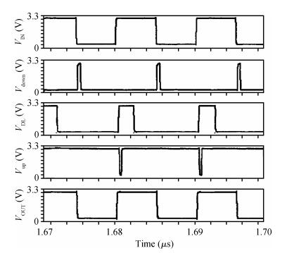
Fig. 2.  Time sequence of some key signals.

Fig. 3.  (a) RS latch-based phase detector. (b) Proposed dynamic phase detector.

Fig. 4.  Time sequence of the phase detector.

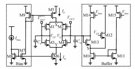
Fig. 5.  Differential charge pump loop.

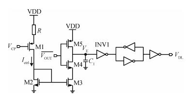
Fig. 6.  Schematic of the delay stage.

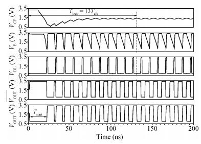
Fig. 7.  Waveform of the charge pump and delay stage transient response at an input of 100 MHz.

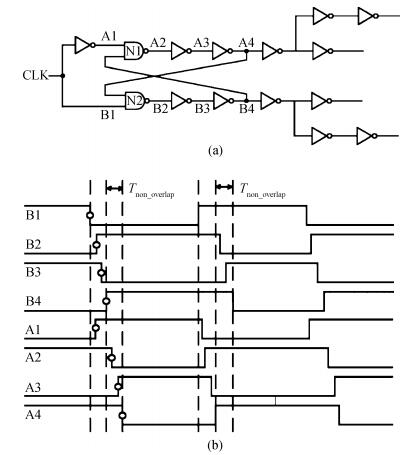
Fig. 8.  Non-overlap clock generator. (a) Proposed circuit. (b) Time sequence.

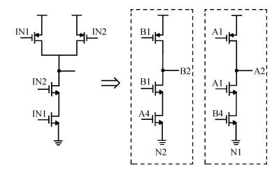
Fig. 9.  Proposed three transistor NAND logic circuit.

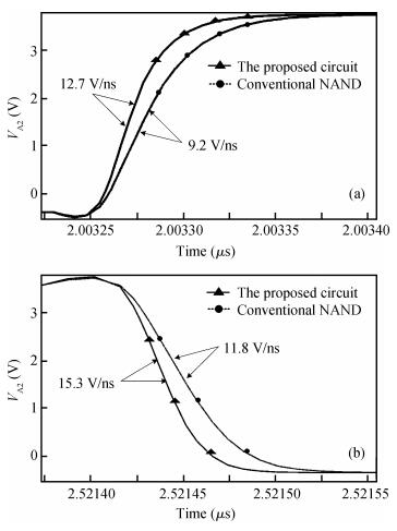
Fig. 10.  (a) Pull-up edge slope at the A2 node. (b) Pull-down edge slope at the A2 node.

Fig. 11.  S-domain model of the proposed PWCL.

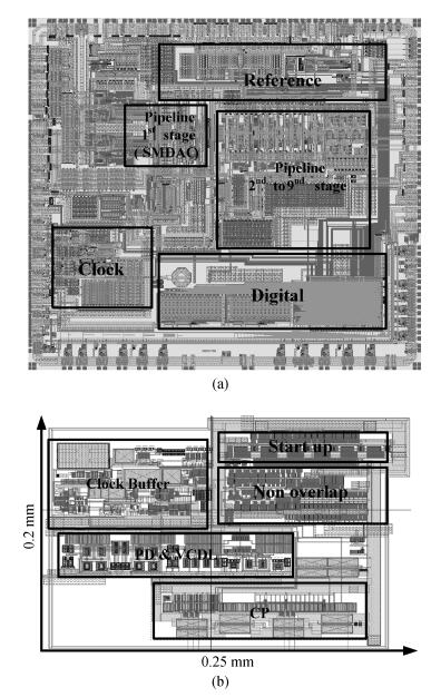
Fig. 12.  Layout of the proposed circuit. (a) The 100-MS/s 14-bit pipeline ADC. (b) The clock generator.

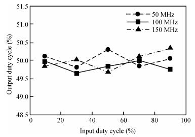
Fig. 13.  Simulation results of a 10%–90% input duty-cycle at 50 MHz, 100 MHz, 150 MHz.

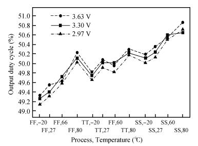
Fig. 14.  Output duty cycle with 30% input duty-cycle at 100 MHz under several PVT corners.

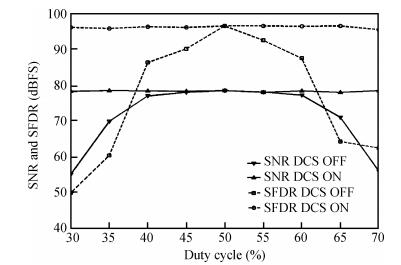
Fig. 15.  SNR and SFDR versus clock duty for a 10 MHz input at 100 MSPS.

Table 1.   Performance comparison.

[1]
Shin D, Kim C, Song J, et al. A 7 ps jitter 0.053 mm fast lock all-digital DLL with a wide range and high resolution DCC. IEEE J Solid-State Circuits, 2009, 44(9):2437 doi: 10.1109/JSSC.2009.2021447
[2]
Weng R M, Liu C Y, Lu Y C. A low jitter DLL-based pulse width control loop with duty cycle adjustment. IEEE Asia Pacific Conference on Circuits and Systems, 2008:418
[3]
Han S R, Liu S I. A 500 MHz-1.25 GHz fast-locking pulsewidth control loop with presentable duty cycle. IEEE J Solid-State Circuits, 2004, 39(3):463 doi: 10.1109/JSSC.2003.822781
[4]
Cheng K H, Su C W, Chang K F. A high linearity, fast-locking pulsewidth control loop with digitally programmable duty cycle correction for wide range operation. IEEE J Solid-State Circuits, 2008, 43(2):399 doi: 10.1109/JSSC.2007.914286
[5]
Lin T H, Chi C C, Chiu W H, et al. A synchronous 50% duty-cycle clock generator in 0.35μm CMOS. IEEE Trans Very Large Scale Integrated Circuits (VLSI) System, 2011, 19(4):585 doi: 10.1109/TVLSI.2009.2037910
[6]
Kao S K, You Y D. Pulse width control loop with low control voltage ripple. Proceedings of the International Multi Conference of Engineers and Computer Scientists, 2012, 2:23 http://www.chinabaike.com/FileUploadDir/autoelectronics/OtherFile/AUCOL_2008JUL24_POT_TA_32.pdf
[7]
Cheng K H, Su C W, Chang K F, et al. A high linearity and fast-locked pulse width control loop with digitally programmable output duty cycle for wide range operation. Proceedings of the 32th European Solid-State Circuits Conference, Montreux, Switzerland, 2006:178
[8]
Navidi M M, Abrishamifar A. A fast lock time pulsewidth control loop using second order passive loop filters. 19th Iranian Conference on Electrical Engineering (ICEE), 2011:1
[9]
Chandrakasan A, Bowhill W J, Fox F. Design of high-performance microprocessor circuit. New York:IEEE Press, 2001
[10]
Zhou X, Wang J, Pang S, et al. A clock management circuit in high-speed pipeline ADC. Electronics & Packaging, 2007, 7(3):20 https://arxiv.org/pdf/0808.0374
[11]
Chen Y G, Tsao H W, Hwang C S. A fast-locking all-digital Deskew buffer with duty-cycle correction. IEEE Trans Very Large Scale Integrated Circuits (VLSI) System, 2012, 99:1 doi: 10.1007%2Fs10470-017-1005-4.pdf
  • Search

    Advanced Search >>

    GET CITATION

    shu

    Export: BibTex EndNote

    Article Metrics

    Article views: 3310 Times PDF downloads: 75 Times Cited by: 0 Times

    History

    Received: 25 May 2012 Revised: 24 September 2012 Online: Published: 01 February 2013

    Catalog

      Email This Article

      User name:
      Email:*请输入正确邮箱
      Code:*验证码错误
      Lei Zhao, Yintang Yang, Zhangming Zhu, Lianxi Liu. A clock generator for a high-speed high-resolution pipelined A/D converter[J]. Journal of Semiconductors, 2013, 34(2): 025003. doi: 10.1088/1674-4926/34/2/025003 ****L Zhao, Y T Yang, Z M Zhu, L X Liu. A clock generator for a high-speed high-resolution pipelined A/D converter[J]. J. Semicond., 2013, 34(2): 025003. doi: 10.1088/1674-4926/34/2/025003.
      Citation:
      Lei Zhao, Yintang Yang, Zhangming Zhu, Lianxi Liu. A clock generator for a high-speed high-resolution pipelined A/D converter[J]. Journal of Semiconductors, 2013, 34(2): 025003. doi: 10.1088/1674-4926/34/2/025003 ****
      L Zhao, Y T Yang, Z M Zhu, L X Liu. A clock generator for a high-speed high-resolution pipelined A/D converter[J]. J. Semicond., 2013, 34(2): 025003. doi: 10.1088/1674-4926/34/2/025003.

      A clock generator for a high-speed high-resolution pipelined A/D converter

      DOI: 10.1088/1674-4926/34/2/025003
      Funds:

      the National High-Tech R & D Program of China 2009AA01Z258

      the Shaanxi Special Major Technological Innovation Program 2009ZKC02-11

      the National Natural Science Foundation of China 60725415

      the National Natural Science Foundation of China 60971066

      Project supported by the National Natural Science Foundation of China (Nos. 60725415, 60971066, 61006028), the National High-Tech R & D Program of China (No. 2009AA01Z258), and the Shaanxi Special Major Technological Innovation Program (No. 2009ZKC02-11)

      the National Natural Science Foundation of China 61006028

      More Information
      • Corresponding author: Zhao Lei, Email:leizhao.ic@gmail.com
      • Received Date: 2012-05-25
      • Revised Date: 2012-09-24
      • Published Date: 2013-02-01

      Catalog

        /

        DownLoad:  Full-Size Img  PowerPoint
        Return
        Return