


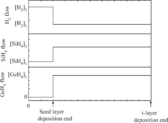
Fig. 1.
Gas flows of the H$_{2}$ , SiH$_{4}$ and GeH$_{4}$ in chamber during i-layer deposition.
SEMICONDUCTOR DEVICES
Yu Cao, Jianjun Zhang, Tianwei Li, Zhenhua Huang, Jun Ma, Xu Yang, Jian Ni, Xinhua Geng and Ying Zhao
Corresponding author: Zhang Jianjun, Email:jjzhang@nankai.edu.cn
Abstract: Using plasma enhanced chemical vapor deposition (PECVD) at 13.56 MHz, a seed layer is fabricated at the initial growth stage of the hydrogenated microcrystalline silicon germanium (μc-Si1-xGex:H) i-layer. The effects of seeding processes on the growth of μc-Si1-xGex:H i-layers and the performance of μc-Si1-xGex:H p-i-n single junction solar cells are investigated. By applying this seeding method, the μc-Si1-xGex:H solar cell shows a significant improvement in short circuit current density (Jsc) and fill factor (FF) with an acceptable performance of blue response as a μc-Si:H solar cell even when the Ge content x increases up to 0.3. Finally, an improved efficiency of 7.05% is achieved for the μc-Si0.7Ge0.3:H solar cell.
Keywords: hydrogenated microcrystalline silicon germanium, seed layer, incubation layer, solar cell
| [1] |
Shah A, Torres P, Tscharner R, et al. Photovoltaic technology:the case for thin-film solar cells. Science, 1999, 285:692 doi: 10.1126/science.285.5428.692
|
| [2] |
Yan B, Yue G, Sivec L, et al. Innovative dual function nc-SiOx:H layer leading to a >16% efficient multi-junction thin-film silicon solar cell. Appl Phys Lett, 2011, 99(11):113512 doi: 10.1063/1.3638068
|
| [3] |
Deng Q W, Wang X L, Xiao H L, et al. Theoretical investigation of efficiency of a p-a-SiC:H/i-a-Si:H/n-μ c-Si solar cell. Journal of Semiconductors, 2010, 31(10):103003 doi: 10.1088/1674-4926/31/10/103003
|
| [4] |
Nawaz M, Ahmad A. Influence of absorber doping in a-SiC:H/a-Si:H/a-SiGe:H solar cells. Journal of Semiconductors, 2007, 33(4):042001 http://www.jos.ac.cn/bdtxbcn/ch/reader/view_abstract.aspx?file_no=11100201&flag=1
|
| [5] |
Ganguly G, Ikeda T, Nishimiya T, et al. Hydrogenated microcrystalline silicon germanium:a bottom cell material for amorphous silicon-based tandem solar cells. Appl Phys Lett, 1996, 69(27):4224 doi: 10.1063/1.116993
|
| [6] |
Zhang J J, Hu Z X, Gu S B, et al. Hydrogenation of polycrystalline SiGe thin film by hot wire technique. Journal of Semiconductors, 2007, 28(3):317 http://www.jos.ac.cn/bdtxbcn/ch/reader/view_abstract.aspx?file_no=06082304&flag=1
|
| [7] |
Zhang L P, Zhang J J, Shang Z R, et al. Influence of reaction gas flows on the properties of SiGe:H thin film prepared by plasma assisted reactive thermal chemical vapour deposition. Chinese Physics B, 2008, 17(9):3448 doi: 10.1088/1674-1056/17/9/051
|
| [8] |
Miyazaki S, Takahashi H, Yamashita H, et al. Growth and characterization of microcrystalline silicon-germanium films. Journal of Non-Crystalline Solids, 2002, 299-302:148 http://www.sciencedirect.com/science/article/pii/S0022309301009486
|
| [9] |
Rath J K, Tichelaar F D, Schropp R E I. Heterogeneous growth of microcrystalline silicon germanium. Solar Energy Materials & Solar Cells, 2002, 74(1-4):553 http://www.sciencedirect.com/science/article/pii/S0927024802000764?via%3Dihub
|
| [10] |
Matsui T, Chang C W, Takada T, et al. Thin film solar cells based on microcrystalline silicon-germanium narrow-gap absorbers. Solar Energy Materials & Solar Cells, 2009, 93(6/7):1100 http://www.sciencedirect.com/science/article/pii/S0927024808004923?via%3Dihub
|
| [11] |
Chang C W, Matsui T, Kondo M. Electron spin resonance study of hydrogenated microcrystalline silicon-germanium alloy thin films. Journal of Non-Crystalline Solids, 2008, 354(19-25):2365 doi: 10.1016/j.jnoncrysol.2007.09.022
|
| [12] |
Filonovich S A, Àguas1 H, Busani T, et al. Hydrogen plasma treatment of very thin p-type nanocrystalline Si films grown by RF-PECVD in the presence of B(CH3)3. Science and Technology of Advanced Materials, 2012, 13(4):045004 doi: 10.1088/1468-6996/13/4/045004
|
| [13] |
Li Y M, Li L, Selvan J A A, et al. Effects of seeding methods on the fabrication of microcrystalline silicon solar cells using radio frequency plasma enhanced chemical vapor deposition. Thin Solid Films, 2005, 483(1/2):84 https://www.researchgate.net/publication/222555580_Effects_of_seeding_methods_on_the_fabrication_of_microcrystalline_silicon_solar_cells_using_radio_frequency_plasma_enhanced_chemical_vapor_deposition
|
| [14] |
Yue G, Yan B, Teplin C, et al. Optimization and characterization of i/p buffer layer in hydrogenated nanocrystalline silicon solar cells. Journal of Non-Crystalline Solids, 2008, 354(19-25):2440 doi: 10.1016/j.jnoncrysol.2007.09.037
|
| [15] |
Zhang H, Zhang X, Wei C, et al. Microstructure characterization of microcrystalline silicon thin films deposited by very high frequency plasma-enhanced chemical vapor deposition by spectroscopic ellipsometry. Thin Solid Films, 2011, 520(2):861 doi: 10.1016/j.tsf.2011.04.166
|
| [16] |
Houben L, Luysberg M, Hapke P, et al. Structural properties of microcrystalline silicon in the transition from highly crystalline to amorphous growth. Philosophical Magazine A, 1998, 77(6):1447 doi: 10.1080/01418619808214262
|
| [17] |
Merten J, Voz C, Munoz A, et al. The role of the buffer layer in the light of a new equivalent circuit for amorphous silicon solar cells. Solar Energy Materials & Solar Cells, 1999, 57(2):153 http://www.sciencedirect.com/science/article/pii/S092702489800169X
|
| [18] |
Tsuo Y S, Xu Y, Ramsay E A, et al. Methods of improving glow-discharge-deposited a-Si1-xGex:H. Materials Research Society Symposium Proceedings, 1991, 219:769 doi: 10.1557/PROC-219-769
|
| [19] |
Liu F Z, Cui J D, Zhang Q F, et al. Dark I-V characteristics and carrier transport mechanism in nano-crystalline Silicon thin film/crystalline silicon hetero-junction solar cells. Journal of Semiconductors, 2008, 29(3):549(in Chinese) http://www.jos.ac.cn/bdtxbcn/ch/reader/view_abstract.aspx?file_no=07062203&flag=1
|
| [20] |
Cleef M W M, Schropp R E I, Rubinelli F A. Significance of tunneling in p+ amorphous silicon carbide n crystalline silicon heterojunction solar cells. Appl Phys Lett, 1998, 73(18):2609 doi: 10.1063/1.122521
|
| [21] |
Sai H, Fujiwara H, Kondo M. Back surface re?ectors with periodic textures fabricated by self-ordering process for light trapping in thin-film microcrystalline silicon solar cells. Solar Energy Materials & Solar Cells, 2009, 93(6/7):1087
|
| [22] |
Das R, Jana T, Ray S. Degradation studies of transparent conducting oxide:a substrate for microcrystalline silicon thin film solar cells. Solar Energy Materials & Solar Cells, 2005, 86(2):207 http://www.sciencedirect.com/science/article/pii/S0927024804002879
|
| [23] |
Müller J, Rech B, Springer J, et al. TCO and light trapping in silicon thin film solar cells. Solar Energy, 2004, 77(6):917 doi: 10.1016/j.solener.2004.03.015
|
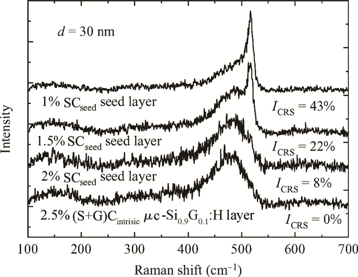
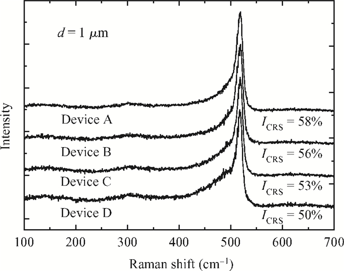
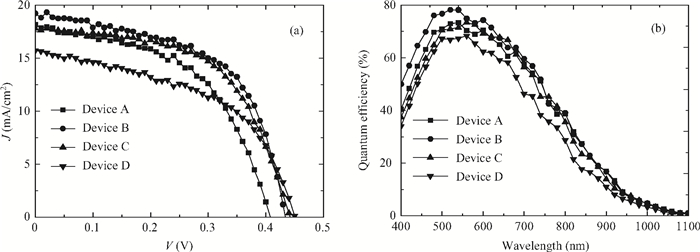
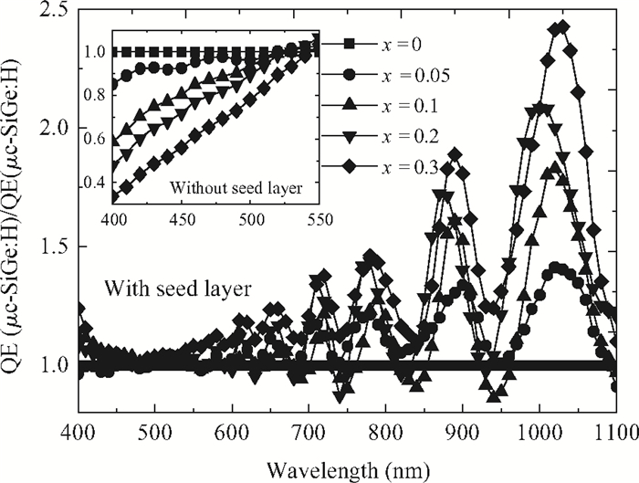
Table 1.
Detailed performance of the

|
| [1] |
Shah A, Torres P, Tscharner R, et al. Photovoltaic technology:the case for thin-film solar cells. Science, 1999, 285:692 doi: 10.1126/science.285.5428.692
|
| [2] |
Yan B, Yue G, Sivec L, et al. Innovative dual function nc-SiOx:H layer leading to a >16% efficient multi-junction thin-film silicon solar cell. Appl Phys Lett, 2011, 99(11):113512 doi: 10.1063/1.3638068
|
| [3] |
Deng Q W, Wang X L, Xiao H L, et al. Theoretical investigation of efficiency of a p-a-SiC:H/i-a-Si:H/n-μ c-Si solar cell. Journal of Semiconductors, 2010, 31(10):103003 doi: 10.1088/1674-4926/31/10/103003
|
| [4] |
Nawaz M, Ahmad A. Influence of absorber doping in a-SiC:H/a-Si:H/a-SiGe:H solar cells. Journal of Semiconductors, 2007, 33(4):042001 http://www.jos.ac.cn/bdtxbcn/ch/reader/view_abstract.aspx?file_no=11100201&flag=1
|
| [5] |
Ganguly G, Ikeda T, Nishimiya T, et al. Hydrogenated microcrystalline silicon germanium:a bottom cell material for amorphous silicon-based tandem solar cells. Appl Phys Lett, 1996, 69(27):4224 doi: 10.1063/1.116993
|
| [6] |
Zhang J J, Hu Z X, Gu S B, et al. Hydrogenation of polycrystalline SiGe thin film by hot wire technique. Journal of Semiconductors, 2007, 28(3):317 http://www.jos.ac.cn/bdtxbcn/ch/reader/view_abstract.aspx?file_no=06082304&flag=1
|
| [7] |
Zhang L P, Zhang J J, Shang Z R, et al. Influence of reaction gas flows on the properties of SiGe:H thin film prepared by plasma assisted reactive thermal chemical vapour deposition. Chinese Physics B, 2008, 17(9):3448 doi: 10.1088/1674-1056/17/9/051
|
| [8] |
Miyazaki S, Takahashi H, Yamashita H, et al. Growth and characterization of microcrystalline silicon-germanium films. Journal of Non-Crystalline Solids, 2002, 299-302:148 http://www.sciencedirect.com/science/article/pii/S0022309301009486
|
| [9] |
Rath J K, Tichelaar F D, Schropp R E I. Heterogeneous growth of microcrystalline silicon germanium. Solar Energy Materials & Solar Cells, 2002, 74(1-4):553 http://www.sciencedirect.com/science/article/pii/S0927024802000764?via%3Dihub
|
| [10] |
Matsui T, Chang C W, Takada T, et al. Thin film solar cells based on microcrystalline silicon-germanium narrow-gap absorbers. Solar Energy Materials & Solar Cells, 2009, 93(6/7):1100 http://www.sciencedirect.com/science/article/pii/S0927024808004923?via%3Dihub
|
| [11] |
Chang C W, Matsui T, Kondo M. Electron spin resonance study of hydrogenated microcrystalline silicon-germanium alloy thin films. Journal of Non-Crystalline Solids, 2008, 354(19-25):2365 doi: 10.1016/j.jnoncrysol.2007.09.022
|
| [12] |
Filonovich S A, Àguas1 H, Busani T, et al. Hydrogen plasma treatment of very thin p-type nanocrystalline Si films grown by RF-PECVD in the presence of B(CH3)3. Science and Technology of Advanced Materials, 2012, 13(4):045004 doi: 10.1088/1468-6996/13/4/045004
|
| [13] |
Li Y M, Li L, Selvan J A A, et al. Effects of seeding methods on the fabrication of microcrystalline silicon solar cells using radio frequency plasma enhanced chemical vapor deposition. Thin Solid Films, 2005, 483(1/2):84 https://www.researchgate.net/publication/222555580_Effects_of_seeding_methods_on_the_fabrication_of_microcrystalline_silicon_solar_cells_using_radio_frequency_plasma_enhanced_chemical_vapor_deposition
|
| [14] |
Yue G, Yan B, Teplin C, et al. Optimization and characterization of i/p buffer layer in hydrogenated nanocrystalline silicon solar cells. Journal of Non-Crystalline Solids, 2008, 354(19-25):2440 doi: 10.1016/j.jnoncrysol.2007.09.037
|
| [15] |
Zhang H, Zhang X, Wei C, et al. Microstructure characterization of microcrystalline silicon thin films deposited by very high frequency plasma-enhanced chemical vapor deposition by spectroscopic ellipsometry. Thin Solid Films, 2011, 520(2):861 doi: 10.1016/j.tsf.2011.04.166
|
| [16] |
Houben L, Luysberg M, Hapke P, et al. Structural properties of microcrystalline silicon in the transition from highly crystalline to amorphous growth. Philosophical Magazine A, 1998, 77(6):1447 doi: 10.1080/01418619808214262
|
| [17] |
Merten J, Voz C, Munoz A, et al. The role of the buffer layer in the light of a new equivalent circuit for amorphous silicon solar cells. Solar Energy Materials & Solar Cells, 1999, 57(2):153 http://www.sciencedirect.com/science/article/pii/S092702489800169X
|
| [18] |
Tsuo Y S, Xu Y, Ramsay E A, et al. Methods of improving glow-discharge-deposited a-Si1-xGex:H. Materials Research Society Symposium Proceedings, 1991, 219:769 doi: 10.1557/PROC-219-769
|
| [19] |
Liu F Z, Cui J D, Zhang Q F, et al. Dark I-V characteristics and carrier transport mechanism in nano-crystalline Silicon thin film/crystalline silicon hetero-junction solar cells. Journal of Semiconductors, 2008, 29(3):549(in Chinese) http://www.jos.ac.cn/bdtxbcn/ch/reader/view_abstract.aspx?file_no=07062203&flag=1
|
| [20] |
Cleef M W M, Schropp R E I, Rubinelli F A. Significance of tunneling in p+ amorphous silicon carbide n crystalline silicon heterojunction solar cells. Appl Phys Lett, 1998, 73(18):2609 doi: 10.1063/1.122521
|
| [21] |
Sai H, Fujiwara H, Kondo M. Back surface re?ectors with periodic textures fabricated by self-ordering process for light trapping in thin-film microcrystalline silicon solar cells. Solar Energy Materials & Solar Cells, 2009, 93(6/7):1087
|
| [22] |
Das R, Jana T, Ray S. Degradation studies of transparent conducting oxide:a substrate for microcrystalline silicon thin film solar cells. Solar Energy Materials & Solar Cells, 2005, 86(2):207 http://www.sciencedirect.com/science/article/pii/S0927024804002879
|
| [23] |
Müller J, Rech B, Springer J, et al. TCO and light trapping in silicon thin film solar cells. Solar Energy, 2004, 77(6):917 doi: 10.1016/j.solener.2004.03.015
|


Article views: 2634 Times PDF downloads: 17 Times Cited by: 0 Times
Received: 12 September 2012 Revised: 19 November 2012 Online: Published: 01 March 2013
| Citation: |
Yu Cao, Jianjun Zhang, Tianwei Li, Zhenhua Huang, Jun Ma, Xu Yang, Jian Ni, Xinhua Geng, Ying Zhao. Effects of seed layer on the performance of microcrystalline silicon germaniumsolar cells[J]. Journal of Semiconductors, 2013, 34(3): 034008. doi: 10.1088/1674-4926/34/3/034008
****
Y Cao, J J Zhang, T W Li, Z H Huang, J Ma, X Yang, J Ni, X H Geng, Y Zhao. Effects of seed layer on the performance of microcrystalline silicon germaniumsolar cells[J]. J. Semicond., 2013, 34(3): 034008. doi: 10.1088/1674-4926/34/3/034008.

|
| [1] |
Shah A, Torres P, Tscharner R, et al. Photovoltaic technology:the case for thin-film solar cells. Science, 1999, 285:692 doi: 10.1126/science.285.5428.692
|
| [2] |
Yan B, Yue G, Sivec L, et al. Innovative dual function nc-SiOx:H layer leading to a >16% efficient multi-junction thin-film silicon solar cell. Appl Phys Lett, 2011, 99(11):113512 doi: 10.1063/1.3638068
|
| [3] |
Deng Q W, Wang X L, Xiao H L, et al. Theoretical investigation of efficiency of a p-a-SiC:H/i-a-Si:H/n-μ c-Si solar cell. Journal of Semiconductors, 2010, 31(10):103003 doi: 10.1088/1674-4926/31/10/103003
|
| [4] |
Nawaz M, Ahmad A. Influence of absorber doping in a-SiC:H/a-Si:H/a-SiGe:H solar cells. Journal of Semiconductors, 2007, 33(4):042001 http://www.jos.ac.cn/bdtxbcn/ch/reader/view_abstract.aspx?file_no=11100201&flag=1
|
| [5] |
Ganguly G, Ikeda T, Nishimiya T, et al. Hydrogenated microcrystalline silicon germanium:a bottom cell material for amorphous silicon-based tandem solar cells. Appl Phys Lett, 1996, 69(27):4224 doi: 10.1063/1.116993
|
| [6] |
Zhang J J, Hu Z X, Gu S B, et al. Hydrogenation of polycrystalline SiGe thin film by hot wire technique. Journal of Semiconductors, 2007, 28(3):317 http://www.jos.ac.cn/bdtxbcn/ch/reader/view_abstract.aspx?file_no=06082304&flag=1
|
| [7] |
Zhang L P, Zhang J J, Shang Z R, et al. Influence of reaction gas flows on the properties of SiGe:H thin film prepared by plasma assisted reactive thermal chemical vapour deposition. Chinese Physics B, 2008, 17(9):3448 doi: 10.1088/1674-1056/17/9/051
|
| [8] |
Miyazaki S, Takahashi H, Yamashita H, et al. Growth and characterization of microcrystalline silicon-germanium films. Journal of Non-Crystalline Solids, 2002, 299-302:148 http://www.sciencedirect.com/science/article/pii/S0022309301009486
|
| [9] |
Rath J K, Tichelaar F D, Schropp R E I. Heterogeneous growth of microcrystalline silicon germanium. Solar Energy Materials & Solar Cells, 2002, 74(1-4):553 http://www.sciencedirect.com/science/article/pii/S0927024802000764?via%3Dihub
|
| [10] |
Matsui T, Chang C W, Takada T, et al. Thin film solar cells based on microcrystalline silicon-germanium narrow-gap absorbers. Solar Energy Materials & Solar Cells, 2009, 93(6/7):1100 http://www.sciencedirect.com/science/article/pii/S0927024808004923?via%3Dihub
|
| [11] |
Chang C W, Matsui T, Kondo M. Electron spin resonance study of hydrogenated microcrystalline silicon-germanium alloy thin films. Journal of Non-Crystalline Solids, 2008, 354(19-25):2365 doi: 10.1016/j.jnoncrysol.2007.09.022
|
| [12] |
Filonovich S A, Àguas1 H, Busani T, et al. Hydrogen plasma treatment of very thin p-type nanocrystalline Si films grown by RF-PECVD in the presence of B(CH3)3. Science and Technology of Advanced Materials, 2012, 13(4):045004 doi: 10.1088/1468-6996/13/4/045004
|
| [13] |
Li Y M, Li L, Selvan J A A, et al. Effects of seeding methods on the fabrication of microcrystalline silicon solar cells using radio frequency plasma enhanced chemical vapor deposition. Thin Solid Films, 2005, 483(1/2):84 https://www.researchgate.net/publication/222555580_Effects_of_seeding_methods_on_the_fabrication_of_microcrystalline_silicon_solar_cells_using_radio_frequency_plasma_enhanced_chemical_vapor_deposition
|
| [14] |
Yue G, Yan B, Teplin C, et al. Optimization and characterization of i/p buffer layer in hydrogenated nanocrystalline silicon solar cells. Journal of Non-Crystalline Solids, 2008, 354(19-25):2440 doi: 10.1016/j.jnoncrysol.2007.09.037
|
| [15] |
Zhang H, Zhang X, Wei C, et al. Microstructure characterization of microcrystalline silicon thin films deposited by very high frequency plasma-enhanced chemical vapor deposition by spectroscopic ellipsometry. Thin Solid Films, 2011, 520(2):861 doi: 10.1016/j.tsf.2011.04.166
|
| [16] |
Houben L, Luysberg M, Hapke P, et al. Structural properties of microcrystalline silicon in the transition from highly crystalline to amorphous growth. Philosophical Magazine A, 1998, 77(6):1447 doi: 10.1080/01418619808214262
|
| [17] |
Merten J, Voz C, Munoz A, et al. The role of the buffer layer in the light of a new equivalent circuit for amorphous silicon solar cells. Solar Energy Materials & Solar Cells, 1999, 57(2):153 http://www.sciencedirect.com/science/article/pii/S092702489800169X
|
| [18] |
Tsuo Y S, Xu Y, Ramsay E A, et al. Methods of improving glow-discharge-deposited a-Si1-xGex:H. Materials Research Society Symposium Proceedings, 1991, 219:769 doi: 10.1557/PROC-219-769
|
| [19] |
Liu F Z, Cui J D, Zhang Q F, et al. Dark I-V characteristics and carrier transport mechanism in nano-crystalline Silicon thin film/crystalline silicon hetero-junction solar cells. Journal of Semiconductors, 2008, 29(3):549(in Chinese) http://www.jos.ac.cn/bdtxbcn/ch/reader/view_abstract.aspx?file_no=07062203&flag=1
|
| [20] |
Cleef M W M, Schropp R E I, Rubinelli F A. Significance of tunneling in p+ amorphous silicon carbide n crystalline silicon heterojunction solar cells. Appl Phys Lett, 1998, 73(18):2609 doi: 10.1063/1.122521
|
| [21] |
Sai H, Fujiwara H, Kondo M. Back surface re?ectors with periodic textures fabricated by self-ordering process for light trapping in thin-film microcrystalline silicon solar cells. Solar Energy Materials & Solar Cells, 2009, 93(6/7):1087
|
| [22] |
Das R, Jana T, Ray S. Degradation studies of transparent conducting oxide:a substrate for microcrystalline silicon thin film solar cells. Solar Energy Materials & Solar Cells, 2005, 86(2):207 http://www.sciencedirect.com/science/article/pii/S0927024804002879
|
| [23] |
Müller J, Rech B, Springer J, et al. TCO and light trapping in silicon thin film solar cells. Solar Energy, 2004, 77(6):917 doi: 10.1016/j.solener.2004.03.015
|

 WeChat ID
Journal of Semiconductors © 2017 All Rights Reserved 京ICP备05085259号-2

 DownLoad:

