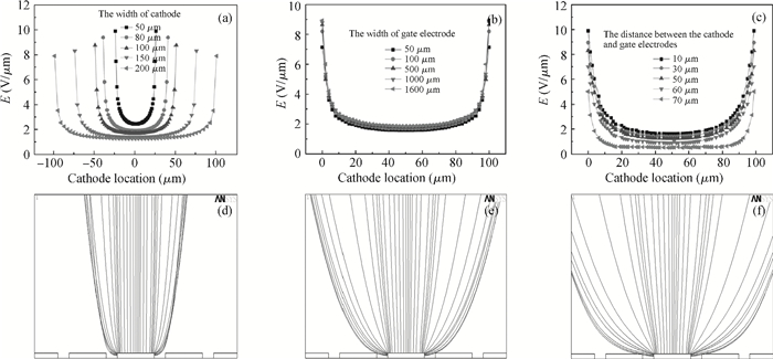
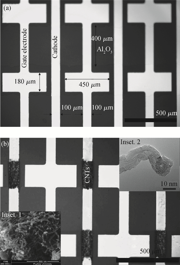
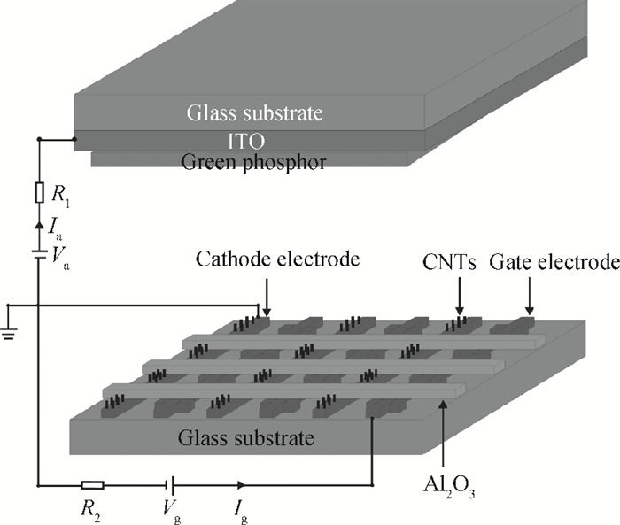
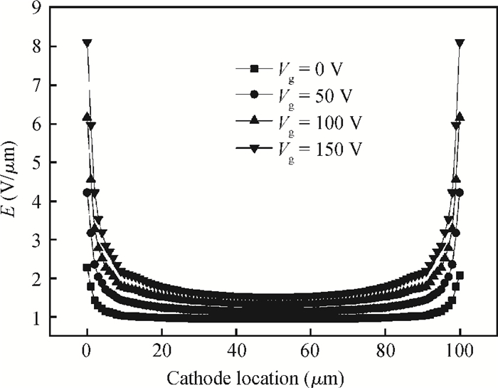
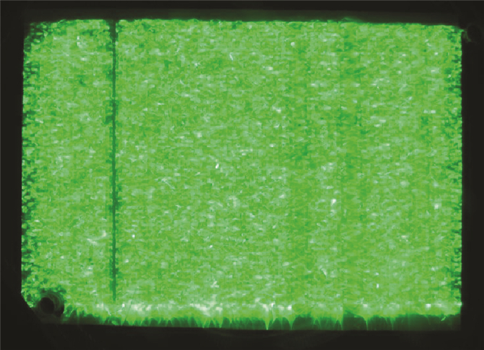
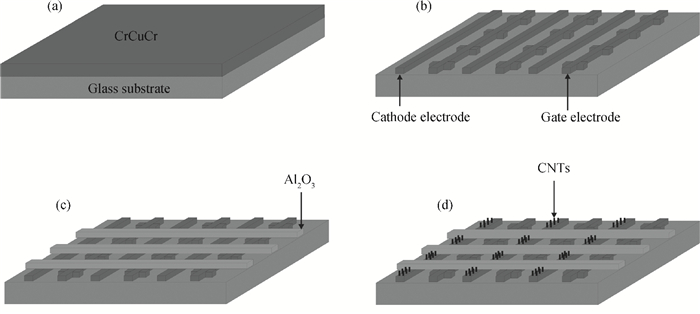
| [1] |
De Heer W A, Chatelain A, Ugarte D. A carbon nanotube field-emission electron source. Science, 1995, 270(5239):1179 doi: 10.1126/science.270.5239.1179 |
| [2] |
Iijima S. Helical microtubules of graphitic carbon. Nature, 1991, 354:56 doi: 10.1038/354056a0 |
| [3] |
Xiao X J, Ye Y, Guo T L, et al. Improved filed emission properties of carbon nanotubes by nickel electroplating and corrosion. Journal of Semiconductors, 2012, 33(5):053004 doi: 10.1088/1674-4926/33/5/053004 |
| [4] |
Zhang Y A, Lin J Y, Guo T L, et al. Stable field emission from planar-gate electron source with CNTs by electrophoretic deposition. Solid-State Electron, 2012, 67(1):6 doi: 10.1016/j.sse.2011.08.005 |
| [5] |
|
| [6] |
Choi W B, Chung D S, Kang J H, et al. Fully sealed, high-brightness carbon-nanotube field-emission display. Appl Phys Lett, 1999, 75(20):3129 doi: 10.1063/1.125253 |
| [7] |
Guo P S, Chen T, Chen Y W, et al. Fabrication of field emission display prototype utilizing printed carbon nanotubes/nanofibers emitters. Solid-State Electron, 2008, 52(6):877 doi: 10.1016/j.sse.2008.01.023 |
| [8] |
Lee S H, Ma C M, Teng C C, et al. The effect of a magnetic field on the graphitization of carbon nanotubes and its application in field emission. Diamond Relat Mater, 2012, 25:111 doi: 10.1016/j.diamond.2012.02.019 |
| [9] |
Choi H Y, Chang W S, Kim H S, et al. Acquisition of X-ray images by using a CNT cold emitter. Phys Lett A, 2006, 357:36 doi: 10.1016/j.physleta.2006.04.015 |
| [10] |
Silan J L, Niemann D L, Ribaya B P, et al. Investigation of carbon nanotube field emitter geometry for increased current density. Solid-State Electron, 2010, 54(12):1543 doi: 10.1016/j.sse.2010.07.004 |
| [11] |
|
| [12] |
|
| [13] |
Jang E S, Goak J C, Lee H S, et al. Light radiation through a transparent cathode plate with single-walled carbon nanotube field emitters. Appl Surf Sci, 2010, 256(22):6838 doi: 10.1016/j.apsusc.2010.04.098 |
| [14] |
Choi Y C, Lee J W, Lee S K, et al. The high contrast ratio and fast response time of a liquid crystal display lit by a carbon nanotube field emission backlight unit. Nanotechnology, 2008, 19(23):235306 doi: 10.1088/0957-4484/19/23/235306 |
| [15] |
Song M S, Park Y K, Yun J J, et al. Distributed circuit model for cold cathode fluorescent lamps in back-light unit of liquid crystal display. Display, 2010, 31(2):104 doi: 10.1016/j.displa.2010.02.006 |
| [16] |
|
| [17] |
Kim Y C, Kang H S, Cho E, et al. Building a backlight unit with lateral gate structure based on carbon nanotube field emitters. Nanotechnology, 2009, 20(9):095204 doi: 10.1088/0957-4484/20/9/095204 |
| [18] |
Wang F H, Lin T C, Tzeng S D, et al. Field emission properties of carbon nanotube cathodes produced using composite plating. Appl Surf Sci, 2010, 256(24):7600 doi: 10.1016/j.apsusc.2010.06.010 |
| [19] |
Park J H, Son G H, Moon J S, et al. Screen printed carbon nanotube field emitter array for lighting source application. J Vac Sci Technol B, 2005, 23(2):749 doi: 10.1116/1.1851535 |
| [20] |
|
| [21] |
Choi Y S, Kang J H, Kim H Y, et al. A simple structure and fabrication of carbon-nanotube field emission display. Appl Surf Sci, 2004, 221(1-4):370 doi: 10.1016/S0169-4332(03)00935-8 |
| [22] |
Zhang Y A, Wu C X, Guo T L, et al. An improved planar-gate triode with CNTs field emitters by electrophoretic deposition. Appl Surf Sci, 2011, 257(8):3259 doi: 10.1016/j.apsusc.2010.10.153 |
| [23] |
|
| [24] |
Su S H, Chiang W T, Lin C C, et al. Multi-wall carbon nanotubes:purification, morphology and field emission performance. Physica E, 2008, 40(7):2322 doi: 10.1016/j.physe.2007.09.087 |
| [25] |
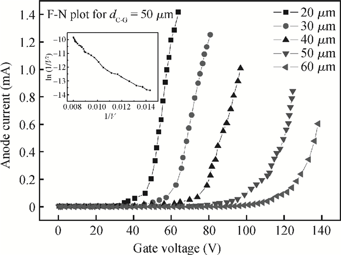
Fowler R H, Nordheim L W. Electron emission in intense electric field. Proc R Soc Lond A, 1999, 173:1928
|


 DownLoad: