


Fig. 1.
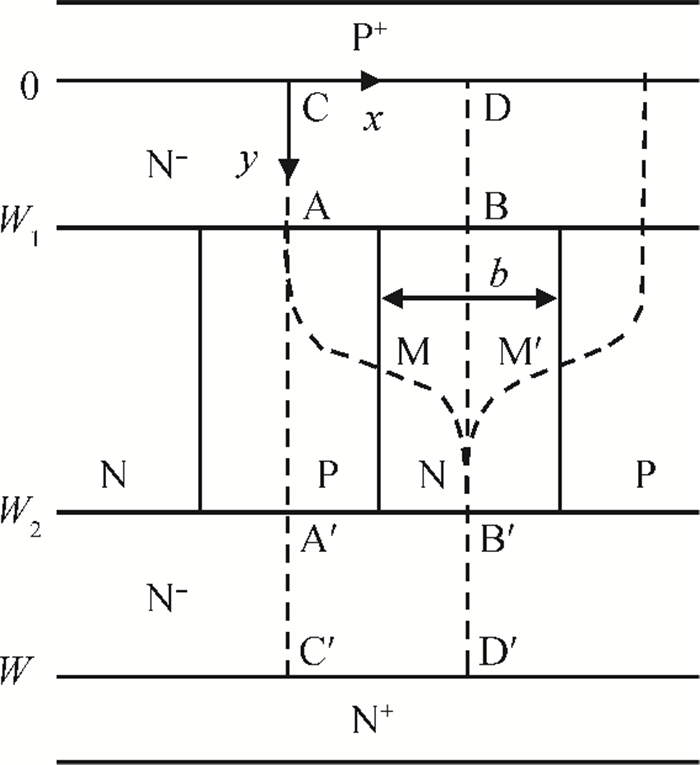
Cross-sectional structure of a buried SJ device. $W_{1}$ and $W_{2}$ are the column positions, and $W$ is the thickness of the drift region.
SEMICONDUCTOR DEVICES
Corresponding author: Huang Haimeng, Email:haimenghuang@126.com
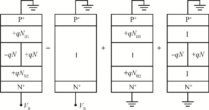
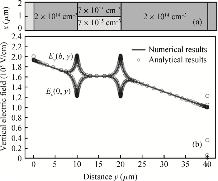
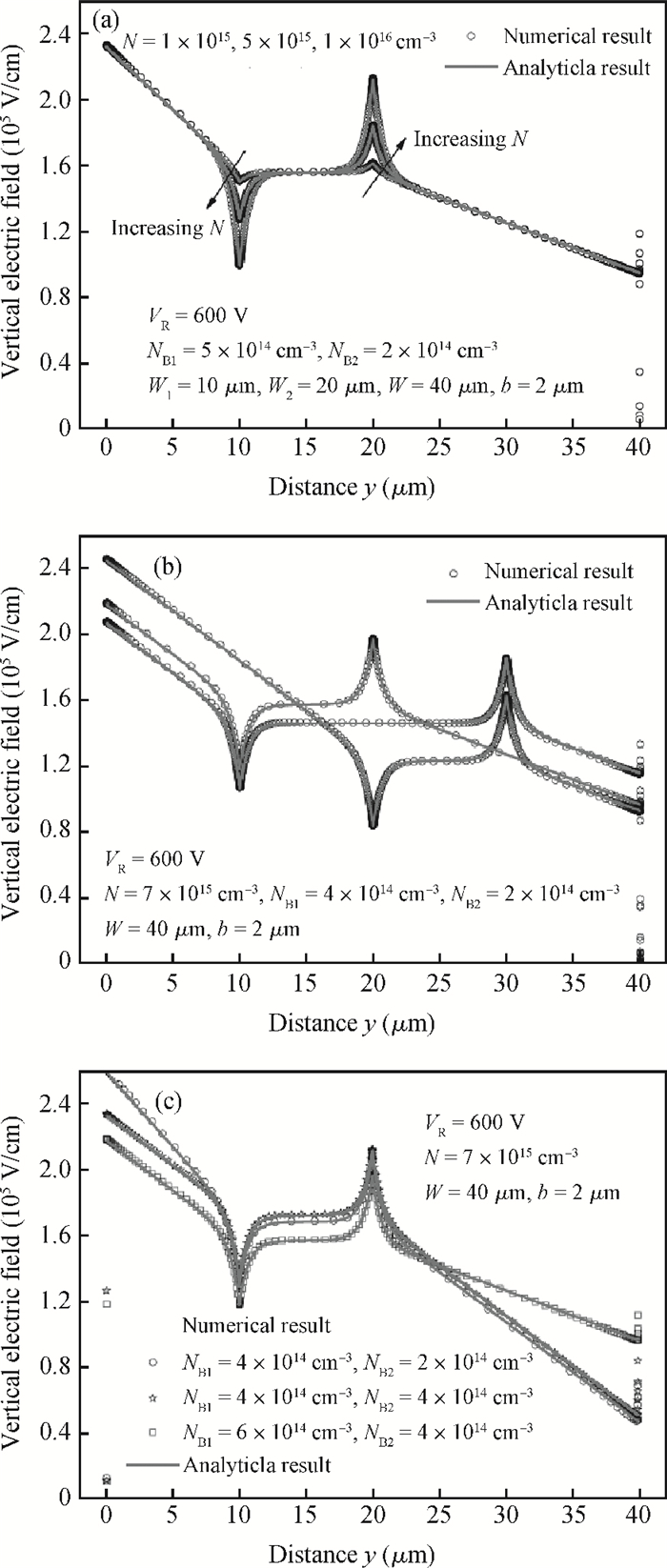
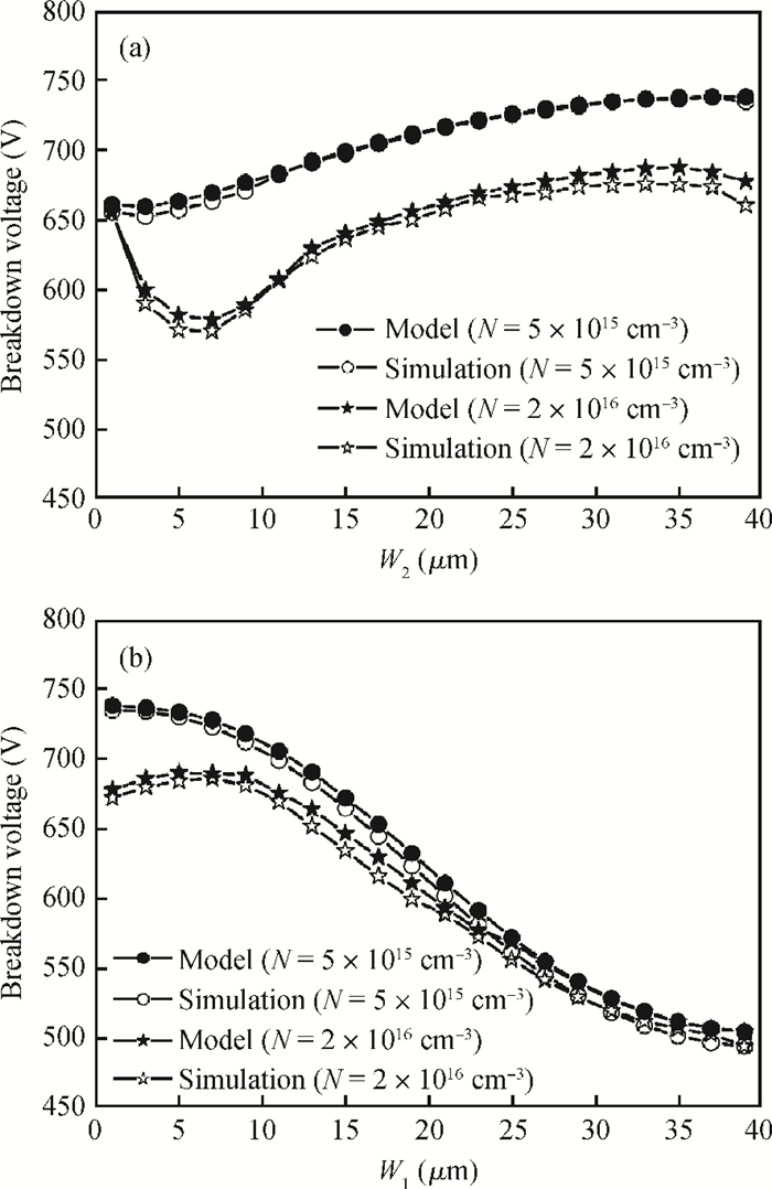
Abstract: An analytical model of the electric field distributions of buried superjunction structures, based on the charge superposition method and Green's function approach, is derived. An accurate approximation of the exact analytical model of the vertical electric field is also proposed and demonstrated by numerical simulation. The influence of the dimension and doping concentration of each layer on the electric field is discussed in detail, and the breakdown voltage is demonstrated by simulations.
Keywords: analytical model, superjunction devices, electric field distributions, breakdown voltage
| [1] |
Coe D J. High voltage semiconductor device. USA Patent, No. 4754310, 1988
|
| [2] |
Chen X B. Semiconductor power devices with alternating conductivity type high voltage breakdown regions. USA Patent, No. 5216275, 1993
|
| [3] |
Chen X B. Theory of a novel voltage-sustaining composite buffer (CB) layer for power devices. Chinese Journal of Electronics, 1998, 7(3):211
|
| [4] |
Lorenz L, Deboy G, Knapp A, et al. COOLMOSTM—a new milestone in high voltage power MOS. Proc ISPSD, 1999:3 http://ieeexplore.ieee.org/document/764028/?reload=true&arnumber=764028&filter%3DAND(p_IS_Number:16497)
|
| [5] |
Saito W, Omura I, Aida S, et al. 600 V semi-superjunction MOSFET. Proc ISPSD, 2003:45
|
| [6] |
Saito W, Omura I, Aida S, et al. Semisuperjunction MOSFETs:new design concept for lower on-resistance and softer reverse-recovery body diode. IEEE Trans Electron Devices, 2003, 50(8):1801 doi: 10.1109/TED.2003.815126
|
| [7] |
Ono S, Saito W, Takashita M, et al. Design concept of n-buffer layer (n-bottom assist layer) for 600 V-class semi-super junction MOSFET. Proc ISPSD, 2007:25
|
| [8] |
Napoli E, Wang H, Udrea F. The effect of charge imbalance on superjunction power devices:an exact analytical solution. IEEE Electron Device Lett, 2008, 29(3):249 doi: 10.1109/LED.2007.915375
|
| [9] |
Wang H, Napoli E, Udrea F. Breakdown voltage for superjunction power devices with charge imbalance:an analytical model valid for both punch through and non punch through devices. IEEE Trans Electron Devices, 2009, 56(12):3175 doi: 10.1109/TED.2009.2032595
|
| [10] |
Synopsys, Taurus Medici User Guide, 2010
|


Article views: 3226 Times PDF downloads: 32 Times Cited by: 0 Times
Received: 17 November 2012 Revised: 19 December 2012 Online: Published: 01 June 2013
| Citation: |
Haimeng Huang, Xingbi Chen. An analytical model of the electric field distributions of buried superjunction devices[J]. Journal of Semiconductors, 2013, 34(6): 064006. doi: 10.1088/1674-4926/34/6/064006
****
H M Huang, X B Chen. An analytical model of the electric field distributions of buried superjunction devices[J]. J. Semicond., 2013, 34(6): 064006. doi: 10.1088/1674-4926/34/6/064006.

|
| [1] |
Coe D J. High voltage semiconductor device. USA Patent, No. 4754310, 1988
|
| [2] |
Chen X B. Semiconductor power devices with alternating conductivity type high voltage breakdown regions. USA Patent, No. 5216275, 1993
|
| [3] |
Chen X B. Theory of a novel voltage-sustaining composite buffer (CB) layer for power devices. Chinese Journal of Electronics, 1998, 7(3):211
|
| [4] |
Lorenz L, Deboy G, Knapp A, et al. COOLMOSTM—a new milestone in high voltage power MOS. Proc ISPSD, 1999:3 http://ieeexplore.ieee.org/document/764028/?reload=true&arnumber=764028&filter%3DAND(p_IS_Number:16497)
|
| [5] |
Saito W, Omura I, Aida S, et al. 600 V semi-superjunction MOSFET. Proc ISPSD, 2003:45
|
| [6] |
Saito W, Omura I, Aida S, et al. Semisuperjunction MOSFETs:new design concept for lower on-resistance and softer reverse-recovery body diode. IEEE Trans Electron Devices, 2003, 50(8):1801 doi: 10.1109/TED.2003.815126
|
| [7] |
Ono S, Saito W, Takashita M, et al. Design concept of n-buffer layer (n-bottom assist layer) for 600 V-class semi-super junction MOSFET. Proc ISPSD, 2007:25
|
| [8] |
Napoli E, Wang H, Udrea F. The effect of charge imbalance on superjunction power devices:an exact analytical solution. IEEE Electron Device Lett, 2008, 29(3):249 doi: 10.1109/LED.2007.915375
|
| [9] |
Wang H, Napoli E, Udrea F. Breakdown voltage for superjunction power devices with charge imbalance:an analytical model valid for both punch through and non punch through devices. IEEE Trans Electron Devices, 2009, 56(12):3175 doi: 10.1109/TED.2009.2032595
|
| [10] |
Synopsys, Taurus Medici User Guide, 2010
|

 WeChat ID
Journal of Semiconductors © 2017 All Rights Reserved 京ICP备05085259号-2

 DownLoad:

