Citation: |
Wei Sun. A low temperature processed Si-quantum-dot poly-Si TFT nonvolatile memory device[J]. Journal of Semiconductors, 2013, 34(6): 064008. doi: 10.1088/1674-4926/34/6/064008
****
W Sun. A low temperature processed Si-quantum-dot poly-Si TFT nonvolatile memory device[J]. J. Semicond., 2013, 34(6): 064008. doi: 10.1088/1674-4926/34/6/064008.
|
A low temperature processed Si-quantum-dot poly-Si TFT nonvolatile memory device
DOI: 10.1088/1674-4926/34/6/064008
More Information
-
Abstract
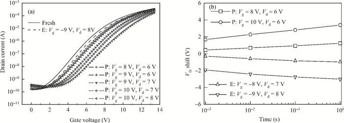
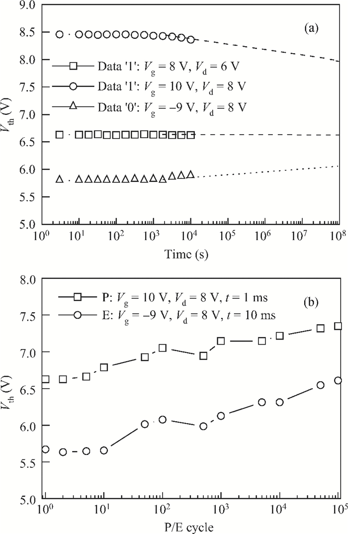
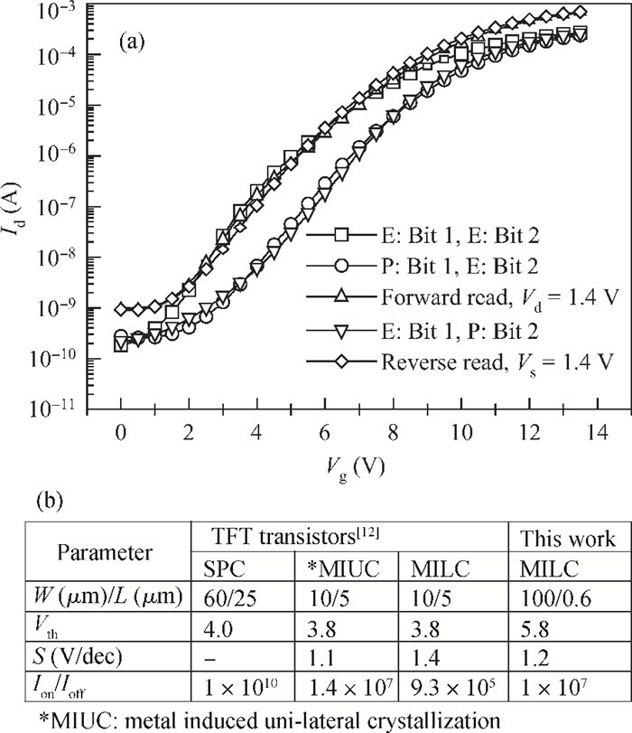
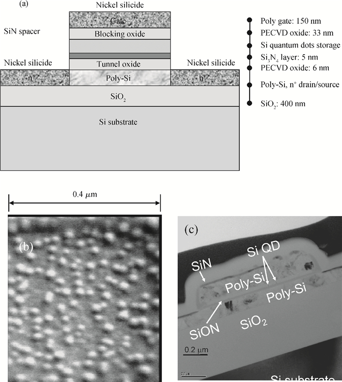
This paper reports on a successful demonstration of poly-Si TFT nonvolatile memory with a much reduced thermal-budget. The TFT uses uniform Si quantum-dots (size 10 nm and density 1011 cm-2) as storage media, obtained via LPCVD by flashing SiH4/H2 at 580℃ for 15 s on a Si3N4 surface. The poly-Si grain-enlargement step was shifted after source/drain formation. The NiSix-silicided source/drain enables a fast lateral-recrystallization, and thus grain-enlargement can be accomplished by a much reduced thermal-cycle (i.e., 550℃/4 h). The excellent memory characteristics suggest that the proposed poly-Si TFT Si quantum-dot memory and associated processes are promising for use in wider TFT applications, such as system-on-glass. -
References
[1] Kagan C R, Andry P. Thin-film transistors. Marcel Dekker, Inc., 2003[2] Wu C, Meng Z, Xiong S, et al. Application of metal induced unilaterally crystallizaed polycrstalline silicon thin-film transistor technology to system-on-glass display. Journal of Non-Cyrstalline Solids, 2006, 352(9-20):1741 doi: 10.1016/j.jnoncrysol.2005.11.150[3] Oh J H, Chung H J, Lee N I, et al. A high-endurance low-temperature polysilicon thin-film transistor EEPROM cell. IEEE Electron Device Lett, 2000, 21(6):304 doi: 10.1109/55.843158[4] Lin Y H, Chien C H, Chou T H, et al. Impact of channel dangling bonds on reliability characteristics of flash memory on poly-Si thin films. IEEE Electron Device Lett, 2007, 28(4):267 doi: 10.1109/LED.2007.891789[5] Lin Y H, Chien C H, Chou T H, et al. Low-temperature polycrystalline silicon thin-film flash memory with hafnium silicate. IEEE Trans Electron Devices, 2007, 54(3):531 doi: 10.1109/TED.2006.890379[6] Lai E K, Lue H T, Hsiao Y H, et al. A multi-layer stackable thin-film transistor (TFT) NAND-type flash memory. IEDM Tech Dig, 2006:41 http://ieeexplore.ieee.org/document/4154322/?reload=true&tp=&arnumber=4154322&contentType=Conference%20Publications&punumber%3D4154162[7] Walker A J, Nallamothu S, Chen E H, et al. 3D TFT-SONOS memory cell for ultra-high density file storage applications. Symp VLSI Technology Digest of Technical Papers, 2003:29 http://ieeexplore.ieee.org/document/1221070/?arnumber=1221070&sortType%3Dasc_p_Sequence%26filter%3DAND(p_IS_Number:27436)[8] Zhan N, Olmedo M, Wang G, et al. Graphene based nickel nanocrystal flash memory. Appl Phys Lett, 2011, 99:113112 doi: 10.1063/1.3640210[9] Wu Y C, Hung M F, Su P W. Improving the performance of nanowires polycrystalline silicon twin thin-film transistors nonvolatile memory by NH3 plasma passivation. J Electrochem Soc, 2011, 158(5):H578 https://www.researchgate.net/publication/274463710_Improving_the_Performance_of_Nanowires_Polycrystalline_Silicon_Twin_Thin-Film_Transistors_Nonvolatile_Memory_by_NH3_Plasma_Passivation[10] Lin Y, Chien C H, Lin C T, et al. High-performance nonvolatile HfO2 nanocrystal memory. IEEE Electron Device Lett, 2005, 26(3):154 doi: 10.1109/LED.2004.842727[11] Chang Y W, Lu T C, Pan S, et al. Modeling for the 2nd-bit effect of a nitride-based trapping storage flash EEPROM cell under two-bit operation. IEEE Electron Device Lett, 2005, 26(3):154 doi: 10.1109/LED.2004.842727[12] Kuo Y. Thin film transistors:material and processes. Vol. 2:Polycrystalline silicon thin film transistor. Kluwer Academic Publisher, 2004 -
Proportional views