


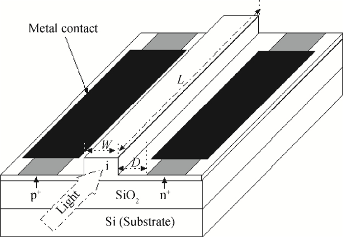
Fig. 1.
Schematic of a silicon rib waveguide with a pin diode.
SEMICONDUCTOR DEVICES
Yong Zhao1, 2, Chao Xu1, Xiaoqing Jiang1, and Huiliang Ge2
Corresponding author: Jiang Xiaoqing, Email:iseejxq@zju.edu.cn
Abstract: The photocurrent effect in pin silicon waveguides at 1550 nm wavelength is experimentally investigated. The photocurrent is mainly attributed to surface-state absorption, defect-state absorption and/or two-photon absorption. Experimental results show that the photocurrent is enhanced by the avalanche effect. A pin silicon waveguide with an intrinsic region width of 3.4 μm and a length of 2000 μm achieves a responsivity of 4.6 mA/W and an avalanche multiplication factor of about five.
Keywords: photodetector, silicon waveguide, photocurrent, avalanche effect
| [1] |
Zimmermann H. Silicon photo-receivers. Topics in Appl Phys, 2004, 94:239 doi: 10.1007/b11504
|
| [2] |
Assefa S, Xia F, Bedell S W, et al. CMOS-integrated high-speed MSM germanium waveguide photodetector. Opt Express, 2010, 18(5):4986 doi: 10.1364/OE.18.004986
|
| [3] |
Liao S, Feng N N, Feng D, et al. 36 GHz submicron silicon waveguide germanium photodetector. Opt Express, 2011, 19(11):10967 doi: 10.1364/OE.19.010967
|
| [4] |
Roucka R, Mathews J, Weng C, et al. High-performance near-IR photodiodes:a novel chemistry-based approach to Ge and Ge-Sn devices integrated on silicon. IEEE J Quantum Electron, 2007, 47(2):213
|
| [5] |
Vivien L, Polzer A, Marris-Morini D, et al. Zero-bias 40 Gbit/s germanium waveguide photodetector on silicon. Opt Express, 2012, 20(2):1096 doi: 10.1364/OE.20.001096
|
| [6] |
Currie M T, Samavedam S B, Langdo T A, et al. Controlling threading dislocation densities in Ge on Si using graded SiGe layers and chemical-mechanical polishing. Appl Phys Lett, 1998, 72(14):1718 doi: 10.1063/1.121162
|
| [7] |
Choi D, Ge Y, Harris J S, et al. Low surface roughness and threading dislocation density Ge growth on Si (001). J Cryst Growth, 2008, 310:4273 doi: 10.1016/j.jcrysgro.2008.07.029
|
| [8] |
Kozlowski G, Yamamoto Y, Bauer J, et al. Selective Ge heteroepitaxy on free-standing Si (001) nanopatterns:a combined Raman, transmission electron microscopy, and finite element method study. J Appl Phys, 2011, 110:053509 doi: 10.1063/1.3631783
|
| [9] |
Baehr-Jones T, Hochberg M, Scherer A. Photodetection in silicon beyond the band edge with surface states. Opt Express, 2008, 16(3):1659 doi: 10.1364/OE.16.001659
|
| [10] |
Chen H, Luo X, Poon A W. Cavity-enhanced photocurrent generation by 1.55μm wavelengths linear absorption in a pin diode embedded silicon microring resonator. Appl Phys Lett, 2009, 95:171111 doi: 10.1063/1.3257384
|
| [11] |
Geis M W, Spector S J, Grein M E, et al. Silicon waveguide infrared photodiodes with > 35 GHz bandwidth and phototransistors with 50 AW-1 response. Opt Express, 2009, 17(7):5193 doi: 10.1364/OE.17.005193
|
| [12] |
Ackert J J, Fiorentino M, Logan D F, et al. Silicon-on-insulator microring resonator defect-based photodetector with 3.5-GHz bandwidth. J Nanophotonics, 2011, 5:059507 doi: 10.1117/1.3666059
|
| [13] |
Casalino M, Sirleto L, Iodice M, et al. Cu/p-Si Schottky barrier-based near infrared photodetector integrated with a silicon-on-insulator waveguide. Appl Phys Lett, 2010, 96:241112 doi: 10.1063/1.3455339
|
| [14] |
Casalino M, Coppola G, Iodice M, et al. Critically coupled silicon Fabry-Perot photodetectors based on the internal photoemission effect at 1550 nm. Opt Express, 2012, 20(11):12599 doi: 10.1364/OE.20.012599
|
| [15] |
Hsieh I, Rong H, Paniccia M. Two-photon-absorption-based optical power monitor in silicon rib waveguides. 7th Group IV Photonics, 2010:326 http://ieeexplore.ieee.org/abstract/document/5643336/
|
| [16] |
Bravo-Abad J, Ippen E P, Soljacic M. Ultrafast photodetection in an all-silicon chip enabled by two-photon absorption. Appl Phys Lett, 2009, 94:241103 doi: 10.1063/1.3155135
|
| [17] |
Chen H, Poon A W. Two-photon absorption photocurrent in p-i-n diode embedded silicon microdisk resonators. Appl Phys Lett, 2010, 94:191106 doi: 10.1063/1.3430548
|
| [18] |
Yamashita Y, Namba K, Nakato Y, et al. Spectroscopic observation of interface states of ultrathin silicon oxide. J Appl Phys, 1996, 79(9):7051 doi: 10.1063/1.361472
|
| [19] |
Fan H Y, Ramdas A K. Infrared absorption and photoconductivity in irradiated silicon. J Appl Phys, 1959, 30(8):1127 doi: 10.1063/1.1735282
|
| [20] |
Cheng L J, Corelli J C, Corbett J W, et al. 1.8-, 3.3-, and 3.9-μm bands in irradiated silicon:correlations with the divacancy. Phys Rev, 1966, 152(2):761 doi: 10.1103/PhysRev.152.761
|
| [21] |
Casalino M, Sirleto L, Moretti L, et al. Design of a silicon re-sonant cavity enhanced photodetector based on the internal photoemission effect at 1.55μm. J Opt A:Pure Appl Opt, 2006, 8:909 doi: 10.1088/1464-4258/8/10/013
|
| [22] |
Zhao Y, Xu C, Wang W, et al. Photocurrent effect in reverse-biased p-n silicon waveguides in communication bands. Chin Phys Lett, 2011, 28(7):074216 doi: 10.1088/0256-307X/28/7/074216
|
| [23] |
Liang T K, Tsang H K, Day I E, et al. Silicon waveguide two-photon absorption detector at 1.5μm wavelength for autocorrelation measurements. Appl Phys Lett, 2002, 81(7):1323 doi: 10.1063/1.1500430
|
| [24] |
Ang T W, Reed G T, Vonsovici A, et al. Effects of grating heights on highly efficient unibond SOI waveguide grating couplers. IEEE Photon Technol Lett, 2000, 12(1):59 doi: 10.1109/68.817493
|
| [25] |
Sze S M, Ng K K. Physics of semiconductor devices. 3rd ed. New York:Wiley, 2007
|
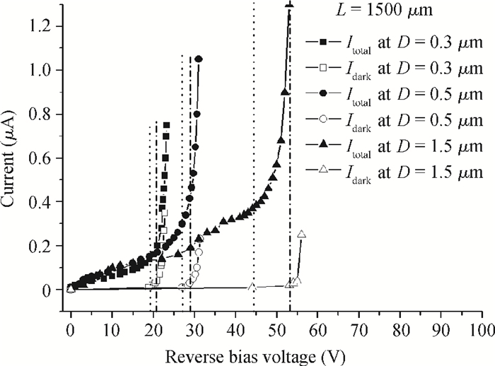
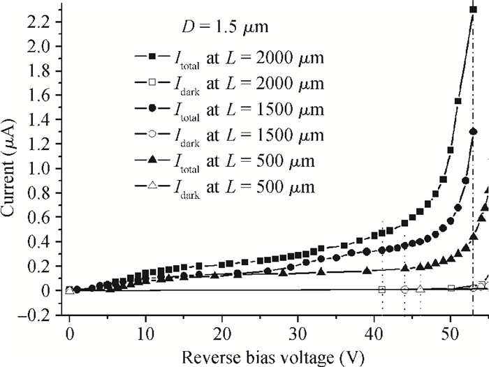
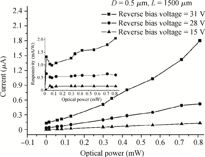
Table 1.
Avalanche multiplication factor (

|
| [1] |
Zimmermann H. Silicon photo-receivers. Topics in Appl Phys, 2004, 94:239 doi: 10.1007/b11504
|
| [2] |
Assefa S, Xia F, Bedell S W, et al. CMOS-integrated high-speed MSM germanium waveguide photodetector. Opt Express, 2010, 18(5):4986 doi: 10.1364/OE.18.004986
|
| [3] |
Liao S, Feng N N, Feng D, et al. 36 GHz submicron silicon waveguide germanium photodetector. Opt Express, 2011, 19(11):10967 doi: 10.1364/OE.19.010967
|
| [4] |
Roucka R, Mathews J, Weng C, et al. High-performance near-IR photodiodes:a novel chemistry-based approach to Ge and Ge-Sn devices integrated on silicon. IEEE J Quantum Electron, 2007, 47(2):213
|
| [5] |
Vivien L, Polzer A, Marris-Morini D, et al. Zero-bias 40 Gbit/s germanium waveguide photodetector on silicon. Opt Express, 2012, 20(2):1096 doi: 10.1364/OE.20.001096
|
| [6] |
Currie M T, Samavedam S B, Langdo T A, et al. Controlling threading dislocation densities in Ge on Si using graded SiGe layers and chemical-mechanical polishing. Appl Phys Lett, 1998, 72(14):1718 doi: 10.1063/1.121162
|
| [7] |
Choi D, Ge Y, Harris J S, et al. Low surface roughness and threading dislocation density Ge growth on Si (001). J Cryst Growth, 2008, 310:4273 doi: 10.1016/j.jcrysgro.2008.07.029
|
| [8] |
Kozlowski G, Yamamoto Y, Bauer J, et al. Selective Ge heteroepitaxy on free-standing Si (001) nanopatterns:a combined Raman, transmission electron microscopy, and finite element method study. J Appl Phys, 2011, 110:053509 doi: 10.1063/1.3631783
|
| [9] |
Baehr-Jones T, Hochberg M, Scherer A. Photodetection in silicon beyond the band edge with surface states. Opt Express, 2008, 16(3):1659 doi: 10.1364/OE.16.001659
|
| [10] |
Chen H, Luo X, Poon A W. Cavity-enhanced photocurrent generation by 1.55μm wavelengths linear absorption in a pin diode embedded silicon microring resonator. Appl Phys Lett, 2009, 95:171111 doi: 10.1063/1.3257384
|
| [11] |
Geis M W, Spector S J, Grein M E, et al. Silicon waveguide infrared photodiodes with > 35 GHz bandwidth and phototransistors with 50 AW-1 response. Opt Express, 2009, 17(7):5193 doi: 10.1364/OE.17.005193
|
| [12] |
Ackert J J, Fiorentino M, Logan D F, et al. Silicon-on-insulator microring resonator defect-based photodetector with 3.5-GHz bandwidth. J Nanophotonics, 2011, 5:059507 doi: 10.1117/1.3666059
|
| [13] |
Casalino M, Sirleto L, Iodice M, et al. Cu/p-Si Schottky barrier-based near infrared photodetector integrated with a silicon-on-insulator waveguide. Appl Phys Lett, 2010, 96:241112 doi: 10.1063/1.3455339
|
| [14] |
Casalino M, Coppola G, Iodice M, et al. Critically coupled silicon Fabry-Perot photodetectors based on the internal photoemission effect at 1550 nm. Opt Express, 2012, 20(11):12599 doi: 10.1364/OE.20.012599
|
| [15] |
Hsieh I, Rong H, Paniccia M. Two-photon-absorption-based optical power monitor in silicon rib waveguides. 7th Group IV Photonics, 2010:326 http://ieeexplore.ieee.org/abstract/document/5643336/
|
| [16] |
Bravo-Abad J, Ippen E P, Soljacic M. Ultrafast photodetection in an all-silicon chip enabled by two-photon absorption. Appl Phys Lett, 2009, 94:241103 doi: 10.1063/1.3155135
|
| [17] |
Chen H, Poon A W. Two-photon absorption photocurrent in p-i-n diode embedded silicon microdisk resonators. Appl Phys Lett, 2010, 94:191106 doi: 10.1063/1.3430548
|
| [18] |
Yamashita Y, Namba K, Nakato Y, et al. Spectroscopic observation of interface states of ultrathin silicon oxide. J Appl Phys, 1996, 79(9):7051 doi: 10.1063/1.361472
|
| [19] |
Fan H Y, Ramdas A K. Infrared absorption and photoconductivity in irradiated silicon. J Appl Phys, 1959, 30(8):1127 doi: 10.1063/1.1735282
|
| [20] |
Cheng L J, Corelli J C, Corbett J W, et al. 1.8-, 3.3-, and 3.9-μm bands in irradiated silicon:correlations with the divacancy. Phys Rev, 1966, 152(2):761 doi: 10.1103/PhysRev.152.761
|
| [21] |
Casalino M, Sirleto L, Moretti L, et al. Design of a silicon re-sonant cavity enhanced photodetector based on the internal photoemission effect at 1.55μm. J Opt A:Pure Appl Opt, 2006, 8:909 doi: 10.1088/1464-4258/8/10/013
|
| [22] |
Zhao Y, Xu C, Wang W, et al. Photocurrent effect in reverse-biased p-n silicon waveguides in communication bands. Chin Phys Lett, 2011, 28(7):074216 doi: 10.1088/0256-307X/28/7/074216
|
| [23] |
Liang T K, Tsang H K, Day I E, et al. Silicon waveguide two-photon absorption detector at 1.5μm wavelength for autocorrelation measurements. Appl Phys Lett, 2002, 81(7):1323 doi: 10.1063/1.1500430
|
| [24] |
Ang T W, Reed G T, Vonsovici A, et al. Effects of grating heights on highly efficient unibond SOI waveguide grating couplers. IEEE Photon Technol Lett, 2000, 12(1):59 doi: 10.1109/68.817493
|
| [25] |
Sze S M, Ng K K. Physics of semiconductor devices. 3rd ed. New York:Wiley, 2007
|


Article views: 3769 Times PDF downloads: 22 Times Cited by: 0 Times
Received: 06 November 2012 Revised: 16 December 2012 Online: Published: 01 June 2013
| Citation: |
Yong Zhao, Chao Xu, Xiaoqing Jiang, Huiliang Ge. Avalanche-enhanced photocurrents in pin silicon waveguides at 1550 nm wavelength[J]. Journal of Semiconductors, 2013, 34(6): 064009. doi: 10.1088/1674-4926/34/6/064009
****
Y Zhao, C Xu, X Q Jiang, H L Ge. Avalanche-enhanced photocurrents in pin silicon waveguides at 1550 nm wavelength[J]. J. Semicond., 2013, 34(6): 064009. doi: 10.1088/1674-4926/34/6/064009.

|
| [1] |
Zimmermann H. Silicon photo-receivers. Topics in Appl Phys, 2004, 94:239 doi: 10.1007/b11504
|
| [2] |
Assefa S, Xia F, Bedell S W, et al. CMOS-integrated high-speed MSM germanium waveguide photodetector. Opt Express, 2010, 18(5):4986 doi: 10.1364/OE.18.004986
|
| [3] |
Liao S, Feng N N, Feng D, et al. 36 GHz submicron silicon waveguide germanium photodetector. Opt Express, 2011, 19(11):10967 doi: 10.1364/OE.19.010967
|
| [4] |
Roucka R, Mathews J, Weng C, et al. High-performance near-IR photodiodes:a novel chemistry-based approach to Ge and Ge-Sn devices integrated on silicon. IEEE J Quantum Electron, 2007, 47(2):213
|
| [5] |
Vivien L, Polzer A, Marris-Morini D, et al. Zero-bias 40 Gbit/s germanium waveguide photodetector on silicon. Opt Express, 2012, 20(2):1096 doi: 10.1364/OE.20.001096
|
| [6] |
Currie M T, Samavedam S B, Langdo T A, et al. Controlling threading dislocation densities in Ge on Si using graded SiGe layers and chemical-mechanical polishing. Appl Phys Lett, 1998, 72(14):1718 doi: 10.1063/1.121162
|
| [7] |
Choi D, Ge Y, Harris J S, et al. Low surface roughness and threading dislocation density Ge growth on Si (001). J Cryst Growth, 2008, 310:4273 doi: 10.1016/j.jcrysgro.2008.07.029
|
| [8] |
Kozlowski G, Yamamoto Y, Bauer J, et al. Selective Ge heteroepitaxy on free-standing Si (001) nanopatterns:a combined Raman, transmission electron microscopy, and finite element method study. J Appl Phys, 2011, 110:053509 doi: 10.1063/1.3631783
|
| [9] |
Baehr-Jones T, Hochberg M, Scherer A. Photodetection in silicon beyond the band edge with surface states. Opt Express, 2008, 16(3):1659 doi: 10.1364/OE.16.001659
|
| [10] |
Chen H, Luo X, Poon A W. Cavity-enhanced photocurrent generation by 1.55μm wavelengths linear absorption in a pin diode embedded silicon microring resonator. Appl Phys Lett, 2009, 95:171111 doi: 10.1063/1.3257384
|
| [11] |
Geis M W, Spector S J, Grein M E, et al. Silicon waveguide infrared photodiodes with > 35 GHz bandwidth and phototransistors with 50 AW-1 response. Opt Express, 2009, 17(7):5193 doi: 10.1364/OE.17.005193
|
| [12] |
Ackert J J, Fiorentino M, Logan D F, et al. Silicon-on-insulator microring resonator defect-based photodetector with 3.5-GHz bandwidth. J Nanophotonics, 2011, 5:059507 doi: 10.1117/1.3666059
|
| [13] |
Casalino M, Sirleto L, Iodice M, et al. Cu/p-Si Schottky barrier-based near infrared photodetector integrated with a silicon-on-insulator waveguide. Appl Phys Lett, 2010, 96:241112 doi: 10.1063/1.3455339
|
| [14] |
Casalino M, Coppola G, Iodice M, et al. Critically coupled silicon Fabry-Perot photodetectors based on the internal photoemission effect at 1550 nm. Opt Express, 2012, 20(11):12599 doi: 10.1364/OE.20.012599
|
| [15] |
Hsieh I, Rong H, Paniccia M. Two-photon-absorption-based optical power monitor in silicon rib waveguides. 7th Group IV Photonics, 2010:326 http://ieeexplore.ieee.org/abstract/document/5643336/
|
| [16] |
Bravo-Abad J, Ippen E P, Soljacic M. Ultrafast photodetection in an all-silicon chip enabled by two-photon absorption. Appl Phys Lett, 2009, 94:241103 doi: 10.1063/1.3155135
|
| [17] |
Chen H, Poon A W. Two-photon absorption photocurrent in p-i-n diode embedded silicon microdisk resonators. Appl Phys Lett, 2010, 94:191106 doi: 10.1063/1.3430548
|
| [18] |
Yamashita Y, Namba K, Nakato Y, et al. Spectroscopic observation of interface states of ultrathin silicon oxide. J Appl Phys, 1996, 79(9):7051 doi: 10.1063/1.361472
|
| [19] |
Fan H Y, Ramdas A K. Infrared absorption and photoconductivity in irradiated silicon. J Appl Phys, 1959, 30(8):1127 doi: 10.1063/1.1735282
|
| [20] |
Cheng L J, Corelli J C, Corbett J W, et al. 1.8-, 3.3-, and 3.9-μm bands in irradiated silicon:correlations with the divacancy. Phys Rev, 1966, 152(2):761 doi: 10.1103/PhysRev.152.761
|
| [21] |
Casalino M, Sirleto L, Moretti L, et al. Design of a silicon re-sonant cavity enhanced photodetector based on the internal photoemission effect at 1.55μm. J Opt A:Pure Appl Opt, 2006, 8:909 doi: 10.1088/1464-4258/8/10/013
|
| [22] |
Zhao Y, Xu C, Wang W, et al. Photocurrent effect in reverse-biased p-n silicon waveguides in communication bands. Chin Phys Lett, 2011, 28(7):074216 doi: 10.1088/0256-307X/28/7/074216
|
| [23] |
Liang T K, Tsang H K, Day I E, et al. Silicon waveguide two-photon absorption detector at 1.5μm wavelength for autocorrelation measurements. Appl Phys Lett, 2002, 81(7):1323 doi: 10.1063/1.1500430
|
| [24] |
Ang T W, Reed G T, Vonsovici A, et al. Effects of grating heights on highly efficient unibond SOI waveguide grating couplers. IEEE Photon Technol Lett, 2000, 12(1):59 doi: 10.1109/68.817493
|
| [25] |
Sze S M, Ng K K. Physics of semiconductor devices. 3rd ed. New York:Wiley, 2007
|

 WeChat ID
Journal of Semiconductors © 2017 All Rights Reserved 京ICP备05085259号-2

 DownLoad:

