


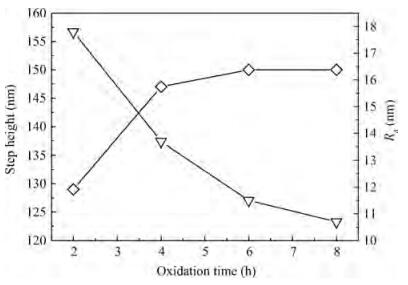
Fig. 1.
A plot of the groove's step heights and average roughness $R_{\rm a}$ of the wafer's wet-etched area versus oxidation time (line with quadrilateral symbol refers to step height and triangle symbol to $R_{\rm a}$ ).
SEMICONDUCTOR TECHNOLOGY
Jinbao Cai, Jinyan Wang, Yang Liu, Zhe Xu, Maojun Wang, Min Yu, Bing Xie and Wengang Wu
Corresponding author: Cai Jinbao, Email:jywang@ime.pku.edu.cn; Wang Jinyan, caijinbaoxd@126.com
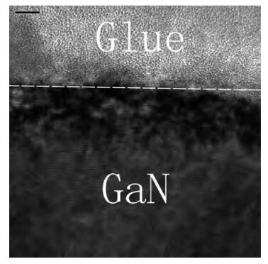
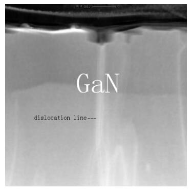
Abstract: A novel wet etching method for AlGaN/GaN heterojunction structures is proposed using thermal oxidation followed by wet etching in KOH solution. It is found that an AlGaN/GaN heterostructure after high temperature oxidation above 700℃ could be etched off in a homothermal (70℃) KOH solution while the KOH solution had no etching effects on the region of the AlGaN/GaN heterostructure protected by a SiO2 layer during the oxidation process. A groove structure with 150 nm step depth on an AlGaN/GaN heterostructure was formed after 8 h thermal oxidation at 900℃ followed by 30 min treatment in 70℃ KOH solution. As the oxidation time increases, the etching depth approaches saturation and the roughness of the etched surface becomes much better. The physical mechanism of this phenomenon is also discussed.
Keywords: AlGaN/GaN, wet etching, thermal oxidation, KOH solution
| [1] |
Hao Y, Yang L, Ma X. High-performance microwave gate-recessed AlGaN/AlN/GaN MOS-HEMT with 73% power-added efficiency. Electron Device Lett, 2011, 32(5):626 doi: 10.1109/LED.2011.2118736
|
| [2] |
Regan S K, Milosavljevic I D. Electron velocity enhancement in laterally scaled GaN DH-HEMTs with ft of 260 GHz. Electron Device Lett, 2011, 32(8):1074 doi: 10.1109/LED.2011.2158386
|
| [3] |
Rowena I B, Selvaraj S L, Egawa T. Buffer thickness contribution to suppress vertical leakage current with high breakdown field (2.3 MV/cm) for GaN on Si. Electron Device Lett, 2011, 32(11):1534 doi: 10.1109/LED.2011.2166052
|
| [4] |
Buttari D, Heikman S, Keller S. Digital etching for highly reproducible low damage gate recessing on AlGaN/GaN HEMTs. IEEE Lester Eastman Conference on High Performance Devices, 2002:461
|
| [5] |
Vartuli C B, Pearton S J, Abernathy C R. Wet chemical etching survey of Ⅲ-nitrides. Solid-State Electron, 1997, 41(12):1947 doi: 10.1016/S0038-1101(97)00173-1
|
| [6] |
Ko C H, Su Y K, Chang S J. Photo-enhanced chemical wet etching of GaN. Mater Sci Eng B, 2002, 96(1):43 doi: 10.1016/S0921-5107(02)00323-9
|
| [7] |
Huang Shengrong, Chen Chao. Research and progress of wet etching for GaN. Micronanotechnology, 2005, 42(6):272
|
| [8] |
Adessida I, Mahajan A, Andideh E. Reactive ion etching of gallium nitride in silicon tetrachloride plasmas. Appl Phys Lett, 1993, 63(20):2777 doi: 10.1063/1.110331
|
| [9] |
Shul R J, McClellan G B, Casalnuovo S A. Inductively coupled plasma etching of GaN. Appl Phys Lett, 1996, 69(8):1119 doi: 10.1063/1.117077
|
| [10] |
Ping A T, Adesida I, Khan M A. Study of chemically assisted ion beam etching of GaN using HCl gas. Appl Phys Lett, 1995, 67(9):1250 doi: 10.1063/1.114387
|
| [11] |
Kawakami R, Inaoka T, Minamoto S. Analysis of GaN etching damage by capacitively coupled RF Ar plasma exposure. Thin Solid Films, 2008, 516(11):3478 doi: 10.1016/j.tsf.2007.08.019
|
| [12] |
Kim H. Reactive ion etching damage in n-GaN and its recovery by post-etch treatment. Electronics Lett, 2008, 44(17):1037 doi: 10.1049/el:20081771
|
| [13] |
Lanford W B, Tanaka T, Otoki Y. Recessed-gate enhancement-mode GaN HEMT with high threshold voltage. Electronics Lett, 2005, 41(7):449 doi: 10.1049/el:20050161
|
| [14] |
Wolter S D, Luther B P, Waltemyer. X-ray photoelectron spectroscopy and X-ray diffraction study of the thermal oxide on gallium nitride. Appl Phys Lett, 1997, 70(16):2156 doi: 10.1063/1.118944
|
| [15] |
Masato H, Ikeda Y, Matsuno T. Novel high drain breakdown voltage AlGaN/GaN HFETs using selective thermal oxidation process. IEDM Technical Digest International, 2000:377
|
| [16] |
Roccaforte F, Giannazzo F, Iucolano F. Electrical behavior of AlGaN/GaN heterostructures upon high-temperature selective oxidation. J Appl Phys, 2009, 106:023703 doi: 10.1063/1.3174438
|
| [17] |
Lee H Y, Huang X Y, Lee C T. Light output enhancement of GaN-based roughened LEDs using bias-assisted photoelectrochemical etching method. J Electrochem Soc, 2008, 155(10):H707
|


Article views: 3276 Times PDF downloads: 43 Times Cited by: 0 Times
Received: 08 January 2013 Revised: 26 January 2013 Online: Published: 01 August 2013
| Citation: |
Jinbao Cai, Jinyan Wang, Yang Liu, Zhe Xu, Maojun Wang, Min Yu, Bing Xie, Wengang Wu. A novel oxidation-based wet etching method for AlGaN/GaN heterostructures[J]. Journal of Semiconductors, 2013, 34(8): 086004. doi: 10.1088/1674-4926/34/8/086004
****
J B Cai, J Y Wang, Y Liu, Z Xu, M J Wang, M Yu, B Xie, W G Wu. A novel oxidation-based wet etching method for AlGaN/GaN heterostructures[J]. J. Semicond., 2013, 34(8): 086004. doi: 10.1088/1674-4926/34/8/086004.

|
| [1] |
Hao Y, Yang L, Ma X. High-performance microwave gate-recessed AlGaN/AlN/GaN MOS-HEMT with 73% power-added efficiency. Electron Device Lett, 2011, 32(5):626 doi: 10.1109/LED.2011.2118736
|
| [2] |
Regan S K, Milosavljevic I D. Electron velocity enhancement in laterally scaled GaN DH-HEMTs with ft of 260 GHz. Electron Device Lett, 2011, 32(8):1074 doi: 10.1109/LED.2011.2158386
|
| [3] |
Rowena I B, Selvaraj S L, Egawa T. Buffer thickness contribution to suppress vertical leakage current with high breakdown field (2.3 MV/cm) for GaN on Si. Electron Device Lett, 2011, 32(11):1534 doi: 10.1109/LED.2011.2166052
|
| [4] |
Buttari D, Heikman S, Keller S. Digital etching for highly reproducible low damage gate recessing on AlGaN/GaN HEMTs. IEEE Lester Eastman Conference on High Performance Devices, 2002:461
|
| [5] |
Vartuli C B, Pearton S J, Abernathy C R. Wet chemical etching survey of Ⅲ-nitrides. Solid-State Electron, 1997, 41(12):1947 doi: 10.1016/S0038-1101(97)00173-1
|
| [6] |
Ko C H, Su Y K, Chang S J. Photo-enhanced chemical wet etching of GaN. Mater Sci Eng B, 2002, 96(1):43 doi: 10.1016/S0921-5107(02)00323-9
|
| [7] |
Huang Shengrong, Chen Chao. Research and progress of wet etching for GaN. Micronanotechnology, 2005, 42(6):272
|
| [8] |
Adessida I, Mahajan A, Andideh E. Reactive ion etching of gallium nitride in silicon tetrachloride plasmas. Appl Phys Lett, 1993, 63(20):2777 doi: 10.1063/1.110331
|
| [9] |
Shul R J, McClellan G B, Casalnuovo S A. Inductively coupled plasma etching of GaN. Appl Phys Lett, 1996, 69(8):1119 doi: 10.1063/1.117077
|
| [10] |
Ping A T, Adesida I, Khan M A. Study of chemically assisted ion beam etching of GaN using HCl gas. Appl Phys Lett, 1995, 67(9):1250 doi: 10.1063/1.114387
|
| [11] |
Kawakami R, Inaoka T, Minamoto S. Analysis of GaN etching damage by capacitively coupled RF Ar plasma exposure. Thin Solid Films, 2008, 516(11):3478 doi: 10.1016/j.tsf.2007.08.019
|
| [12] |
Kim H. Reactive ion etching damage in n-GaN and its recovery by post-etch treatment. Electronics Lett, 2008, 44(17):1037 doi: 10.1049/el:20081771
|
| [13] |
Lanford W B, Tanaka T, Otoki Y. Recessed-gate enhancement-mode GaN HEMT with high threshold voltage. Electronics Lett, 2005, 41(7):449 doi: 10.1049/el:20050161
|
| [14] |
Wolter S D, Luther B P, Waltemyer. X-ray photoelectron spectroscopy and X-ray diffraction study of the thermal oxide on gallium nitride. Appl Phys Lett, 1997, 70(16):2156 doi: 10.1063/1.118944
|
| [15] |
Masato H, Ikeda Y, Matsuno T. Novel high drain breakdown voltage AlGaN/GaN HFETs using selective thermal oxidation process. IEDM Technical Digest International, 2000:377
|
| [16] |
Roccaforte F, Giannazzo F, Iucolano F. Electrical behavior of AlGaN/GaN heterostructures upon high-temperature selective oxidation. J Appl Phys, 2009, 106:023703 doi: 10.1063/1.3174438
|
| [17] |
Lee H Y, Huang X Y, Lee C T. Light output enhancement of GaN-based roughened LEDs using bias-assisted photoelectrochemical etching method. J Electrochem Soc, 2008, 155(10):H707
|

 WeChat ID
Journal of Semiconductors © 2017 All Rights Reserved 京ICP备05085259号-2

 DownLoad:

