


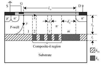
Fig. 1.
Schematic cross section of CK SOI structure
SEMICONDUCTOR DEVICES
Jie Fan, Bo Zhang, Xiaorong Luo, Zhigang Wang and Zhaoji Li
Corresponding author: Fan Jie, Email:fan576@163.com
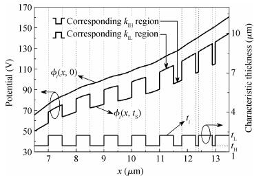
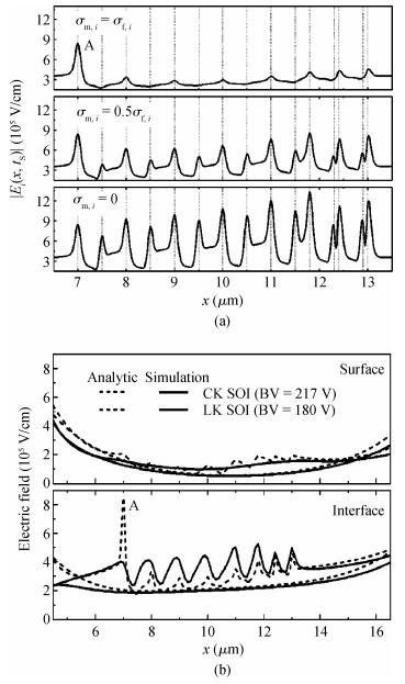
Abstract: An analytical model for a novel high voltage silicon-on-insulator device with composite-k (relative permittivity) dielectric buried layer (CK SOI) is proposed. In this structure, the composite-k buried layer is composed by alternating Si3N4 and low-k (k=2.65) dielectric in the lateral direction. Due to the composite-k buried layer, the breakdown voltage (BV) is improved both by the vertical and lateral direction. Taking the modulation effect of accumulated interface holes into account, an analytical model is developed. In the blocking state, the proposed model revealed the mechanism of hole accumulation above the Si3N4 buried layer and investigated the modulation effect of accumulated holes on the two-dimensional (2-D) potential and electric field distributions. This analytical model is verified by the simulation results. Compared with the low-k dielectric buried layer SOI (LK SOI), simulation results show that the BV for CK SOI is enhanced by 21% and the specific on-resistance is reduced by 32%, respectively.
Keywords: composite-k dielectric, accumulated holes, potential well, electric field, SOI
| [1] |
Cristoloveanu S. Silicon on insulator technologies and devices:from present to future. Solid-State Electron, 2001, 45:1403 doi: 10.1016/S0038-1101(00)00271-9
|
| [2] |
Nakagawa A, Yasuhara N, Omura I, et al. Prospects of high voltage power ICs on thin SOI. IEEE IEDM Tech Dig, 1992:229
|
| [3] |
Merchant S, Arnold E, Baumgart H, et al. Realization of high breakdown voltage (> 700 V) in thin SOI devices. Proc ISPSD, 1991:31
|
| [4] |
Luo J, Cao G, Ekkanath Madathil S N, et al. A high performance RF LDMOSFET in thin film SOI technology with step drift profile. Solid-State Electron, 2003, 47:1937 doi: 10.1016/S0038-1101(03)00222-3
|
| [5] |
Zhu R, Khemka V, Khan T, et al. A high voltage super-junction NLDMOS device implemented in 0.13μm SOI based smart power IC technology. Proc ISPSD, 2010:79
|
| [6] |
Darbandy G, Lime F, Cerdeira A, et al. Study of potential high-k dielectric for UTB SOI MOSFETs using analytical modeling of the gate tunneling leakage. Semicond Sci Technol, 2011, 26:115002 doi: 10.1088/0268-1242/26/11/115002
|
| [7] |
Zhang S, Sin J K O, Lai T M L, et al. Numerical Modeling of linear doping profiles for high-voltage thin-film SOI devices. IEEE Trans Electron Devices, 1999, 46(5):1036 doi: 10.1109/16.760414
|
| [8] |
Hu X, Zhang B, Luo X, et al. Analytical models for the electric field distributions and breakdown voltage of triple RESURF SOI LDMOS. Solid-State Electron, 2012, 69:89 doi: 10.1016/j.sse.2011.12.010
|
| [9] |
Zhang B, Li Z, Hu S, et al. Field enhancement for dielectric layer of high-voltage devices on silicon on insulator. IEEE Trans Electron Devices, 2009, 56(10):2327 doi: 10.1109/TED.2009.2028405
|
| [10] |
Gao Huanmei, Luo Xiaorong, Zhang Wei, et al. A new integrated SOI power device based on self-isolation technology. Journal of Semiconductors, 2010, 31(8):084012 doi: 10.1088/1674-4926/31/8/084012
|
| [11] |
Ge Rui, Luo Xiaorong, Jiang Yongheng, et al. A low on-resistance SOI LDMOS using a trench gate and a recessed drain. Journal of Semiconductors, 2012, 33(7):074005 doi: 10.1088/1674-4926/33/7/074005
|
| [12] |
Luo Xiaorong, Hu Gangyi, Zhou Kun, et al. High voltage SOI LDMOS with a compound buried layer. Journal of Semiconductors, 2012, 33(10):104003 doi: 10.1088/1674-4926/33/10/104003
|
| [13] |
Guo Y, Li Z, Zhang B. A new analytical model for optimizing SOI LDMOS with step doped drift region. Microelectron J, 2006, 37:861 doi: 10.1016/j.mejo.2006.03.004
|
| [14] |
Chung S K, Shin D K. An analytical model for interaction of SIPOS layer with underlying silicon of SOI RESURF devices. IEEE Trans Electron Devices, 1999, 46(8):1804 doi: 10.1109/16.777174
|
| [15] |
Chung S K. An analytical model for breakdown voltage of surface implanted SOI RESURF LDMOS. IEEE Trans Electron Devices, 2000, 47(5):1006 doi: 10.1109/16.841233
|
| [16] |
Guo Yufeng, Li Zhaoji, Zhang Bo, et al. Breakdown model and new structure of SOI high voltage devices with step buried oxide fixed charges. Journal of Semiconductors, 2004, 25(12):1695
|
| [17] |
Luo X, Wang Y, Deng H, et al. Novel low-k dielectric buried-layer high-voltage LDMOS on partial SOI. IEEE Trans Electron Devices, 2010, 57(2):535 doi: 10.1109/TED.2009.2037372
|
| [18] |
Luo X, Zhang B, Li Z. A new structure and its analytical model for the electric field and breakdown voltage of SOI high voltage device with variable-k dielectric buried layer. Solid-State Electron, 2007, 51:493 doi: 10.1016/j.sse.2007.01.034
|
| [19] |
Luo X, Udrea F, Wang Y, et al. Partial SOI power LDMOS with a variable low-k dielectric buried layer and a buried P layer. IEEE Electron Device Lett, 2010, 31(6):594 doi: 10.1109/LED.2010.2046616
|
| [20] |
Lubguban J Jr., Saitoh A, Kurata Y, et al. Stability of the dielectric properties of PECVD deposited carbon-doped SiOF films. Thin Solid Films, 1999, 337:67 doi: 10.1016/S0040-6090(98)01186-9
|
| [21] |
Wang P F, Ding S J, Zhang J Y, et al. Low-dielectric-constant α -SiCOF film for ULSI interconnection prepared by PECVD with TEOS/C4F8/O2. Appl Phys A, 2001, 72:721 doi: 10.1007/s003390000562
|


Article views: 2823 Times PDF downloads: 10 Times Cited by: 0 Times
Received: 18 February 2013 Revised: 19 March 2013 Online: Published: 01 September 2013
| Citation: |
Jie Fan, Bo Zhang, Xiaorong Luo, Zhigang Wang, Zhaoji Li. Analytical model for high-voltage SOI device with composite-k dielectric buried layer[J]. Journal of Semiconductors, 2013, 34(9): 094008. doi: 10.1088/1674-4926/34/9/094008
****
J Fan, B Zhang, X R Luo, Z G Wang, Z J Li. Analytical model for high-voltage SOI device with composite-k dielectric buried layer[J]. J. Semicond., 2013, 34(9): 094008. doi: 10.1088/1674-4926/34/9/094008.

|
| [1] |
Cristoloveanu S. Silicon on insulator technologies and devices:from present to future. Solid-State Electron, 2001, 45:1403 doi: 10.1016/S0038-1101(00)00271-9
|
| [2] |
Nakagawa A, Yasuhara N, Omura I, et al. Prospects of high voltage power ICs on thin SOI. IEEE IEDM Tech Dig, 1992:229
|
| [3] |
Merchant S, Arnold E, Baumgart H, et al. Realization of high breakdown voltage (> 700 V) in thin SOI devices. Proc ISPSD, 1991:31
|
| [4] |
Luo J, Cao G, Ekkanath Madathil S N, et al. A high performance RF LDMOSFET in thin film SOI technology with step drift profile. Solid-State Electron, 2003, 47:1937 doi: 10.1016/S0038-1101(03)00222-3
|
| [5] |
Zhu R, Khemka V, Khan T, et al. A high voltage super-junction NLDMOS device implemented in 0.13μm SOI based smart power IC technology. Proc ISPSD, 2010:79
|
| [6] |
Darbandy G, Lime F, Cerdeira A, et al. Study of potential high-k dielectric for UTB SOI MOSFETs using analytical modeling of the gate tunneling leakage. Semicond Sci Technol, 2011, 26:115002 doi: 10.1088/0268-1242/26/11/115002
|
| [7] |
Zhang S, Sin J K O, Lai T M L, et al. Numerical Modeling of linear doping profiles for high-voltage thin-film SOI devices. IEEE Trans Electron Devices, 1999, 46(5):1036 doi: 10.1109/16.760414
|
| [8] |
Hu X, Zhang B, Luo X, et al. Analytical models for the electric field distributions and breakdown voltage of triple RESURF SOI LDMOS. Solid-State Electron, 2012, 69:89 doi: 10.1016/j.sse.2011.12.010
|
| [9] |
Zhang B, Li Z, Hu S, et al. Field enhancement for dielectric layer of high-voltage devices on silicon on insulator. IEEE Trans Electron Devices, 2009, 56(10):2327 doi: 10.1109/TED.2009.2028405
|
| [10] |
Gao Huanmei, Luo Xiaorong, Zhang Wei, et al. A new integrated SOI power device based on self-isolation technology. Journal of Semiconductors, 2010, 31(8):084012 doi: 10.1088/1674-4926/31/8/084012
|
| [11] |
Ge Rui, Luo Xiaorong, Jiang Yongheng, et al. A low on-resistance SOI LDMOS using a trench gate and a recessed drain. Journal of Semiconductors, 2012, 33(7):074005 doi: 10.1088/1674-4926/33/7/074005
|
| [12] |
Luo Xiaorong, Hu Gangyi, Zhou Kun, et al. High voltage SOI LDMOS with a compound buried layer. Journal of Semiconductors, 2012, 33(10):104003 doi: 10.1088/1674-4926/33/10/104003
|
| [13] |
Guo Y, Li Z, Zhang B. A new analytical model for optimizing SOI LDMOS with step doped drift region. Microelectron J, 2006, 37:861 doi: 10.1016/j.mejo.2006.03.004
|
| [14] |
Chung S K, Shin D K. An analytical model for interaction of SIPOS layer with underlying silicon of SOI RESURF devices. IEEE Trans Electron Devices, 1999, 46(8):1804 doi: 10.1109/16.777174
|
| [15] |
Chung S K. An analytical model for breakdown voltage of surface implanted SOI RESURF LDMOS. IEEE Trans Electron Devices, 2000, 47(5):1006 doi: 10.1109/16.841233
|
| [16] |
Guo Yufeng, Li Zhaoji, Zhang Bo, et al. Breakdown model and new structure of SOI high voltage devices with step buried oxide fixed charges. Journal of Semiconductors, 2004, 25(12):1695
|
| [17] |
Luo X, Wang Y, Deng H, et al. Novel low-k dielectric buried-layer high-voltage LDMOS on partial SOI. IEEE Trans Electron Devices, 2010, 57(2):535 doi: 10.1109/TED.2009.2037372
|
| [18] |
Luo X, Zhang B, Li Z. A new structure and its analytical model for the electric field and breakdown voltage of SOI high voltage device with variable-k dielectric buried layer. Solid-State Electron, 2007, 51:493 doi: 10.1016/j.sse.2007.01.034
|
| [19] |
Luo X, Udrea F, Wang Y, et al. Partial SOI power LDMOS with a variable low-k dielectric buried layer and a buried P layer. IEEE Electron Device Lett, 2010, 31(6):594 doi: 10.1109/LED.2010.2046616
|
| [20] |
Lubguban J Jr., Saitoh A, Kurata Y, et al. Stability of the dielectric properties of PECVD deposited carbon-doped SiOF films. Thin Solid Films, 1999, 337:67 doi: 10.1016/S0040-6090(98)01186-9
|
| [21] |
Wang P F, Ding S J, Zhang J Y, et al. Low-dielectric-constant α -SiCOF film for ULSI interconnection prepared by PECVD with TEOS/C4F8/O2. Appl Phys A, 2001, 72:721 doi: 10.1007/s003390000562
|

 WeChat ID
Journal of Semiconductors © 2017 All Rights Reserved 京ICP备05085259号-2

 DownLoad:

