


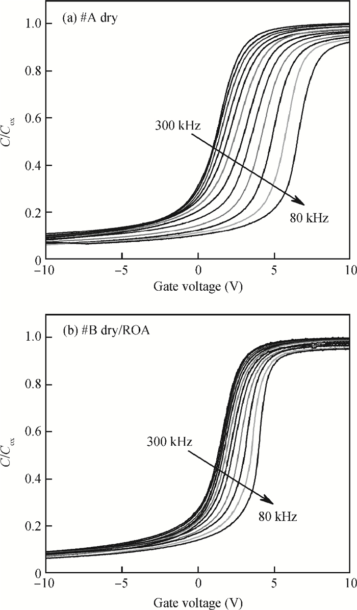
Fig. 1.
Temperature-dependent $C$ -$V$ curves of samples (a) #A and (b) #B.
SEMICONDUCTOR DEVICES
Corresponding author: Wang Dejun, dwang121@dlut.edu.cn
Abstract: The effects of wet re-oxidation annealing (wet-ROA) on the shallow interface traps of n-type 4H-SiC metal-oxide-semiconductor (MOS) capacitors were investigated by Gray-Brown method and angle-dependent X-ray photoelectron spectroscopy technique. The results present the energy distribution of the density of interface traps ($D_{\rm it})$ from 0 to 0.2 eV below SiC conduction band edge ($E_{\rm C})$ of the sample with wet-ROA for the first time, and indicate that wet-ROA could reduce the $D_{\rm it}$ in this energy range by more than 60%. The reduction in $D_{\rm it}$ is attributed to the reaction between the introduced oxygen and the SiO$_{x}$C$_{y}$ species, which results in C release and SiO$_{x}$C$_{y}$ transformation into higher oxidation states, thus reducing the SiO$_{x}$C$_{y}$ content and the SiO$_{x}$C$_{y}$ interface transition region thickness.
Keywords: SiC, MOS, shallow interface traps, wet-ROA, interface transition region
| [1] |
Palmour J W, Edmond J A, Kong H S, et al. 6H-silicon carbide devices and applications. Physica B, 1993, 185:461 doi: 10.1016/0921-4526(93)90278-E
|
| [2] |
Cooper J A Jr. Advances in SiC technology. Phys Status Solidi A, 1997, 162:305 doi: 10.1002/(ISSN)1521-396X
|
| [3] |
Yano H, Hirao T, Kimoto T, et al. A cause for highly improved channel mobility of 4H-SiC metal-oxide-semiconductor field-effect transistors on the (1120) face. Appl Phys Lett, 2001, 78(3):374 doi: 10.1063/1.1340861
|
| [4] |
Chen Z. Recent progress in SiC power electronic devices and fabrication process. Chinese Journal of Semiconductors, 2002, 23(7):673(in Chinese) http://adsabs.harvard.edu/abs/1997PSSBR.202..605Y
|
| [5] |
Schörner R, Friedrichs P, Peters D, et al. Significantly improved performance of MOSFET's on silicon carbide using the 15R-SiC polytype. IEEE Electron Device Lett, 1999, 20(5):241 doi: 10.1109/55.761027
|
| [6] |
Afanas'ev V V, Bassler M, Pensl G, et al. Intrinsic SiC/SiO2 interface states. Phys Status Solidi A, 1997, 162:321 doi: 10.1002/(ISSN)1521-396X
|
| [7] |
Das M K, Um B S, Cooper J A Jr. Anomalously high density of interface states near the conduction band in SiO2/4H-SiC MOS devices. Mater Sci Forum, 2000, 338-342:1069 doi: 10.4028/www.scientific.net/MSF.338-342
|
| [8] |
Saks N S, Mani S S, Agarwal A K. Interface trap profile near the band edges at the 4H-SiC/SiO2 interface. Appl Phys Lett, 2000, 76(16):2250 doi: 10.1063/1.126311
|
| [9] |
Pensl G, Beljakowa S, Frank T, et al. Alternative techniques to reduce interface traps in n-type 4H-SiC MOS capacitors. Phys Status Solidi B, 2008, 245(7):1378 doi: 10.1002/pssb.v245:7
|
| [10] |
Hornetz B, Michel H J, Halbritter J. Oxidation and 6H-SiC-SiO2 interface. J Vac Sci Technol A, 1995, 13(3):767 doi: 10.1116/1.579824
|
| [11] |
Zhu Q, Huang L, Li W, et al. Chemical structure study of SiO2/4H-SiC (0001) interface transition region by angle-dependent X-ray photoelectron spectroscopy. Appl Phys Lett, 2011, 99:082102 doi: 10.1063/1.3628322
|
| [12] |
Wang D, Zhao L, Zhu Q, et al. A transition region study of SiO2/4H-SiC interface by ADXPS. Journal of Semiconductors, 2008, 29(5):944(in Chinese) https://infoscience.epfl.ch/record/141739
|
| [13] |
Lipkin L A, Palmour J W. Improved oxidation procedures for reduced SiO2/SiC defects. J Electron Mater, 1996, 25(5):909 doi: 10.1007/BF02666657
|
| [14] |
Suzuki S, Harada S, Kosugi R, et al. Correlation between channel mobility and shallow interface traps in SiC metal-oxide-semiconductor field-effect transistors. J Appl Phys, 2002, 92(10):6230 doi: 10.1063/1.1513210
|
| [15] |
Gray P V, Brown D M. Density of SiO2-Si interface states. Appl Phys Lett, 1966, 8(2):31 doi: 10.1063/1.1754468
|
| [16] |
Taoka N, Mizubayashi W, Morita Y, et al. Effect of Ge metal-insulator-semiconductor interfacial layers on interface trap density near the conduction band edge. Jpn J Appl Phys, 2010, 49:04DA09 http://adsabs.harvard.edu/abs/1998SSEle..42..477C
|
| [17] |
Dhar S, Chen X D, Mooney P M, et al. Ultrashallow defect states at SiO2/4H-SiC interfaces. Appl Phys Lett, 2008, 92:102112 doi: 10.1063/1.2898502
|
| [18] |
Zhu X, Ahyi A C, Li M, et al. The effects of nitrogen plasma anneals on interface trap density and channel mobility for 4H-SiC MOS devices. Solid-State Electron, 2011, 57:76 doi: 10.1016/j.sse.2010.12.002
|
| [19] |
Zhu Q, Qin F, Li W, et al. Improvement of SiO2/4H-SiC interface properties by electron cyclotron resonance microwave nitrogen-hydrogen mixed plasma post-oxidation annealing. Appl Phys Lett, 2013, 103:062105 doi: 10.1063/1.4818141
|
| [20] |
Sze S M. Physics of semiconductor devices. New York: Wiley, 1991
|
| [21] |
Önneby C, Pantano C G. Silicon oxycarbide formation on SiC surfaces and at the SiC/SiO2 interface. J Vac Sci Technol A, 1997, 15(3):1597 doi: 10.1116/1.580951
|
| [22] |
Hill J M, Royce D G, Fadley C S, et al. Properties of oxidized silicon as determined by angular-dependent X-ray photoelectron spectroscopy. Chem Phys Lett, 1976, 44(2):225 doi: 10.1016/0009-2614(76)80496-4
|
| [23] |
Fulghum J E. Determination of overlayer thickness by angle-resolved XPS:a comparison of algorithms. Surf Interface Anal, 1993, 20:161 doi: 10.1002/(ISSN)1096-9918
|
| [24] |
Tanuma S, Powell C J, Penn D R. Calculations of electron inelastic mean free paths. Surf Interface Anal, 1991, 17:927 doi: 10.1002/(ISSN)1096-9918
|
| [25] |
Beccat P, Silva P D, Huiban Y, et al. Quantitative surface analysis by XPS:application to hydrotreating catalysts. Oil & Gas Sci Tech-Rev. IFP, 1999, 54(4):487 https://ogst.ifpenergiesnouvelles.fr/articles/ogst/pdf/1999/04/beccat_v54n4.pdf
|
Table 1. The atomic percentages of Si, O, and C and the atomic ratio of O/Si and C/Si of samples #A1 and #B1.

|
| [1] |
Palmour J W, Edmond J A, Kong H S, et al. 6H-silicon carbide devices and applications. Physica B, 1993, 185:461 doi: 10.1016/0921-4526(93)90278-E
|
| [2] |
Cooper J A Jr. Advances in SiC technology. Phys Status Solidi A, 1997, 162:305 doi: 10.1002/(ISSN)1521-396X
|
| [3] |
Yano H, Hirao T, Kimoto T, et al. A cause for highly improved channel mobility of 4H-SiC metal-oxide-semiconductor field-effect transistors on the (1120) face. Appl Phys Lett, 2001, 78(3):374 doi: 10.1063/1.1340861
|
| [4] |
Chen Z. Recent progress in SiC power electronic devices and fabrication process. Chinese Journal of Semiconductors, 2002, 23(7):673(in Chinese) http://adsabs.harvard.edu/abs/1997PSSBR.202..605Y
|
| [5] |
Schörner R, Friedrichs P, Peters D, et al. Significantly improved performance of MOSFET's on silicon carbide using the 15R-SiC polytype. IEEE Electron Device Lett, 1999, 20(5):241 doi: 10.1109/55.761027
|
| [6] |
Afanas'ev V V, Bassler M, Pensl G, et al. Intrinsic SiC/SiO2 interface states. Phys Status Solidi A, 1997, 162:321 doi: 10.1002/(ISSN)1521-396X
|
| [7] |
Das M K, Um B S, Cooper J A Jr. Anomalously high density of interface states near the conduction band in SiO2/4H-SiC MOS devices. Mater Sci Forum, 2000, 338-342:1069 doi: 10.4028/www.scientific.net/MSF.338-342
|
| [8] |
Saks N S, Mani S S, Agarwal A K. Interface trap profile near the band edges at the 4H-SiC/SiO2 interface. Appl Phys Lett, 2000, 76(16):2250 doi: 10.1063/1.126311
|
| [9] |
Pensl G, Beljakowa S, Frank T, et al. Alternative techniques to reduce interface traps in n-type 4H-SiC MOS capacitors. Phys Status Solidi B, 2008, 245(7):1378 doi: 10.1002/pssb.v245:7
|
| [10] |
Hornetz B, Michel H J, Halbritter J. Oxidation and 6H-SiC-SiO2 interface. J Vac Sci Technol A, 1995, 13(3):767 doi: 10.1116/1.579824
|
| [11] |
Zhu Q, Huang L, Li W, et al. Chemical structure study of SiO2/4H-SiC (0001) interface transition region by angle-dependent X-ray photoelectron spectroscopy. Appl Phys Lett, 2011, 99:082102 doi: 10.1063/1.3628322
|
| [12] |
Wang D, Zhao L, Zhu Q, et al. A transition region study of SiO2/4H-SiC interface by ADXPS. Journal of Semiconductors, 2008, 29(5):944(in Chinese) https://infoscience.epfl.ch/record/141739
|
| [13] |
Lipkin L A, Palmour J W. Improved oxidation procedures for reduced SiO2/SiC defects. J Electron Mater, 1996, 25(5):909 doi: 10.1007/BF02666657
|
| [14] |
Suzuki S, Harada S, Kosugi R, et al. Correlation between channel mobility and shallow interface traps in SiC metal-oxide-semiconductor field-effect transistors. J Appl Phys, 2002, 92(10):6230 doi: 10.1063/1.1513210
|
| [15] |
Gray P V, Brown D M. Density of SiO2-Si interface states. Appl Phys Lett, 1966, 8(2):31 doi: 10.1063/1.1754468
|
| [16] |
Taoka N, Mizubayashi W, Morita Y, et al. Effect of Ge metal-insulator-semiconductor interfacial layers on interface trap density near the conduction band edge. Jpn J Appl Phys, 2010, 49:04DA09 http://adsabs.harvard.edu/abs/1998SSEle..42..477C
|
| [17] |
Dhar S, Chen X D, Mooney P M, et al. Ultrashallow defect states at SiO2/4H-SiC interfaces. Appl Phys Lett, 2008, 92:102112 doi: 10.1063/1.2898502
|
| [18] |
Zhu X, Ahyi A C, Li M, et al. The effects of nitrogen plasma anneals on interface trap density and channel mobility for 4H-SiC MOS devices. Solid-State Electron, 2011, 57:76 doi: 10.1016/j.sse.2010.12.002
|
| [19] |
Zhu Q, Qin F, Li W, et al. Improvement of SiO2/4H-SiC interface properties by electron cyclotron resonance microwave nitrogen-hydrogen mixed plasma post-oxidation annealing. Appl Phys Lett, 2013, 103:062105 doi: 10.1063/1.4818141
|
| [20] |
Sze S M. Physics of semiconductor devices. New York: Wiley, 1991
|
| [21] |
Önneby C, Pantano C G. Silicon oxycarbide formation on SiC surfaces and at the SiC/SiO2 interface. J Vac Sci Technol A, 1997, 15(3):1597 doi: 10.1116/1.580951
|
| [22] |
Hill J M, Royce D G, Fadley C S, et al. Properties of oxidized silicon as determined by angular-dependent X-ray photoelectron spectroscopy. Chem Phys Lett, 1976, 44(2):225 doi: 10.1016/0009-2614(76)80496-4
|
| [23] |
Fulghum J E. Determination of overlayer thickness by angle-resolved XPS:a comparison of algorithms. Surf Interface Anal, 1993, 20:161 doi: 10.1002/(ISSN)1096-9918
|
| [24] |
Tanuma S, Powell C J, Penn D R. Calculations of electron inelastic mean free paths. Surf Interface Anal, 1991, 17:927 doi: 10.1002/(ISSN)1096-9918
|
| [25] |
Beccat P, Silva P D, Huiban Y, et al. Quantitative surface analysis by XPS:application to hydrotreating catalysts. Oil & Gas Sci Tech-Rev. IFP, 1999, 54(4):487 https://ogst.ifpenergiesnouvelles.fr/articles/ogst/pdf/1999/04/beccat_v54n4.pdf
|


Article views: 2895 Times PDF downloads: 21 Times Cited by: 0 Times
Received: 10 July 2013 Revised: 21 August 2013 Online: Published: 01 February 2014
| Citation: |
Qiaozhi Zhu, Dejun Wang. Effects of wet-ROA on shallow interface traps of n-type 4H-SiC MOS capacitors[J]. Journal of Semiconductors, 2014, 35(2): 024002. doi: 10.1088/1674-4926/35/2/024002
****
Q Z Zhu, D J Wang. Effects of wet-ROA on shallow interface traps of n-type 4H-SiC MOS capacitors[J]. J. Semicond., 2014, 35(2): 024002. doi: 10.1088/1674-4926/35/2/024002.

|
| [1] |
Palmour J W, Edmond J A, Kong H S, et al. 6H-silicon carbide devices and applications. Physica B, 1993, 185:461 doi: 10.1016/0921-4526(93)90278-E
|
| [2] |
Cooper J A Jr. Advances in SiC technology. Phys Status Solidi A, 1997, 162:305 doi: 10.1002/(ISSN)1521-396X
|
| [3] |
Yano H, Hirao T, Kimoto T, et al. A cause for highly improved channel mobility of 4H-SiC metal-oxide-semiconductor field-effect transistors on the (1120) face. Appl Phys Lett, 2001, 78(3):374 doi: 10.1063/1.1340861
|
| [4] |
Chen Z. Recent progress in SiC power electronic devices and fabrication process. Chinese Journal of Semiconductors, 2002, 23(7):673(in Chinese) http://adsabs.harvard.edu/abs/1997PSSBR.202..605Y
|
| [5] |
Schörner R, Friedrichs P, Peters D, et al. Significantly improved performance of MOSFET's on silicon carbide using the 15R-SiC polytype. IEEE Electron Device Lett, 1999, 20(5):241 doi: 10.1109/55.761027
|
| [6] |
Afanas'ev V V, Bassler M, Pensl G, et al. Intrinsic SiC/SiO2 interface states. Phys Status Solidi A, 1997, 162:321 doi: 10.1002/(ISSN)1521-396X
|
| [7] |
Das M K, Um B S, Cooper J A Jr. Anomalously high density of interface states near the conduction band in SiO2/4H-SiC MOS devices. Mater Sci Forum, 2000, 338-342:1069 doi: 10.4028/www.scientific.net/MSF.338-342
|
| [8] |
Saks N S, Mani S S, Agarwal A K. Interface trap profile near the band edges at the 4H-SiC/SiO2 interface. Appl Phys Lett, 2000, 76(16):2250 doi: 10.1063/1.126311
|
| [9] |
Pensl G, Beljakowa S, Frank T, et al. Alternative techniques to reduce interface traps in n-type 4H-SiC MOS capacitors. Phys Status Solidi B, 2008, 245(7):1378 doi: 10.1002/pssb.v245:7
|
| [10] |
Hornetz B, Michel H J, Halbritter J. Oxidation and 6H-SiC-SiO2 interface. J Vac Sci Technol A, 1995, 13(3):767 doi: 10.1116/1.579824
|
| [11] |
Zhu Q, Huang L, Li W, et al. Chemical structure study of SiO2/4H-SiC (0001) interface transition region by angle-dependent X-ray photoelectron spectroscopy. Appl Phys Lett, 2011, 99:082102 doi: 10.1063/1.3628322
|
| [12] |
Wang D, Zhao L, Zhu Q, et al. A transition region study of SiO2/4H-SiC interface by ADXPS. Journal of Semiconductors, 2008, 29(5):944(in Chinese) https://infoscience.epfl.ch/record/141739
|
| [13] |
Lipkin L A, Palmour J W. Improved oxidation procedures for reduced SiO2/SiC defects. J Electron Mater, 1996, 25(5):909 doi: 10.1007/BF02666657
|
| [14] |
Suzuki S, Harada S, Kosugi R, et al. Correlation between channel mobility and shallow interface traps in SiC metal-oxide-semiconductor field-effect transistors. J Appl Phys, 2002, 92(10):6230 doi: 10.1063/1.1513210
|
| [15] |
Gray P V, Brown D M. Density of SiO2-Si interface states. Appl Phys Lett, 1966, 8(2):31 doi: 10.1063/1.1754468
|
| [16] |
Taoka N, Mizubayashi W, Morita Y, et al. Effect of Ge metal-insulator-semiconductor interfacial layers on interface trap density near the conduction band edge. Jpn J Appl Phys, 2010, 49:04DA09 http://adsabs.harvard.edu/abs/1998SSEle..42..477C
|
| [17] |
Dhar S, Chen X D, Mooney P M, et al. Ultrashallow defect states at SiO2/4H-SiC interfaces. Appl Phys Lett, 2008, 92:102112 doi: 10.1063/1.2898502
|
| [18] |
Zhu X, Ahyi A C, Li M, et al. The effects of nitrogen plasma anneals on interface trap density and channel mobility for 4H-SiC MOS devices. Solid-State Electron, 2011, 57:76 doi: 10.1016/j.sse.2010.12.002
|
| [19] |
Zhu Q, Qin F, Li W, et al. Improvement of SiO2/4H-SiC interface properties by electron cyclotron resonance microwave nitrogen-hydrogen mixed plasma post-oxidation annealing. Appl Phys Lett, 2013, 103:062105 doi: 10.1063/1.4818141
|
| [20] |
Sze S M. Physics of semiconductor devices. New York: Wiley, 1991
|
| [21] |
Önneby C, Pantano C G. Silicon oxycarbide formation on SiC surfaces and at the SiC/SiO2 interface. J Vac Sci Technol A, 1997, 15(3):1597 doi: 10.1116/1.580951
|
| [22] |
Hill J M, Royce D G, Fadley C S, et al. Properties of oxidized silicon as determined by angular-dependent X-ray photoelectron spectroscopy. Chem Phys Lett, 1976, 44(2):225 doi: 10.1016/0009-2614(76)80496-4
|
| [23] |
Fulghum J E. Determination of overlayer thickness by angle-resolved XPS:a comparison of algorithms. Surf Interface Anal, 1993, 20:161 doi: 10.1002/(ISSN)1096-9918
|
| [24] |
Tanuma S, Powell C J, Penn D R. Calculations of electron inelastic mean free paths. Surf Interface Anal, 1991, 17:927 doi: 10.1002/(ISSN)1096-9918
|
| [25] |
Beccat P, Silva P D, Huiban Y, et al. Quantitative surface analysis by XPS:application to hydrotreating catalysts. Oil & Gas Sci Tech-Rev. IFP, 1999, 54(4):487 https://ogst.ifpenergiesnouvelles.fr/articles/ogst/pdf/1999/04/beccat_v54n4.pdf
|

 WeChat ID
Journal of Semiconductors © 2017 All Rights Reserved 京ICP备05085259号-2

 DownLoad:

