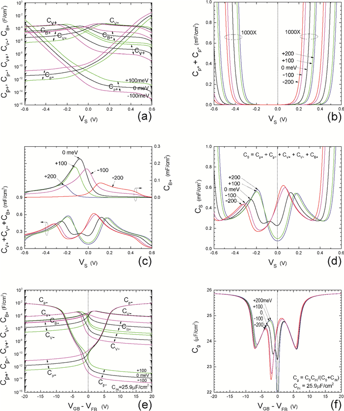
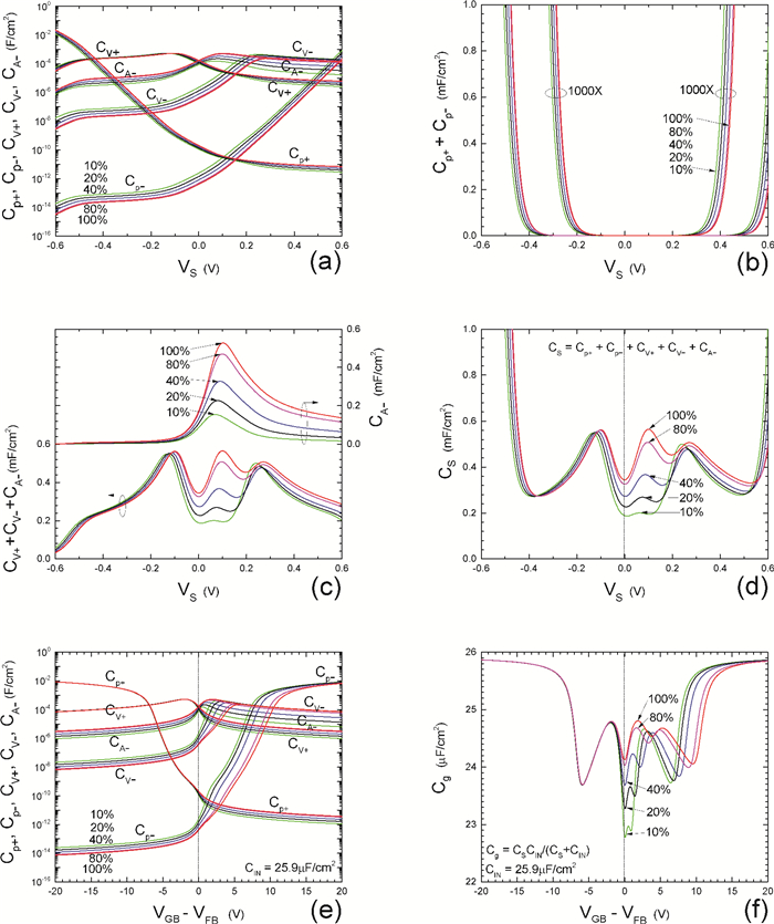
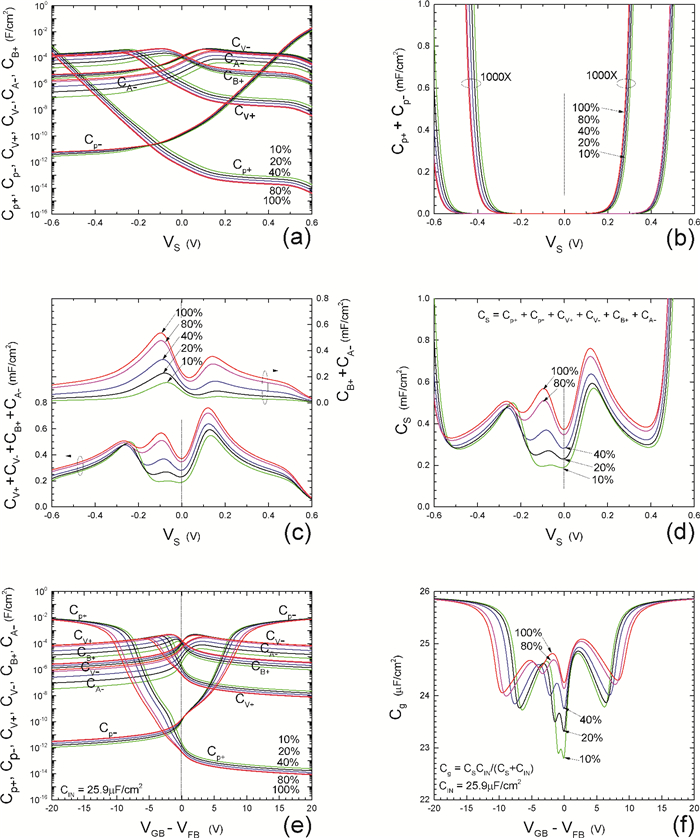
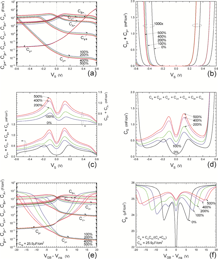
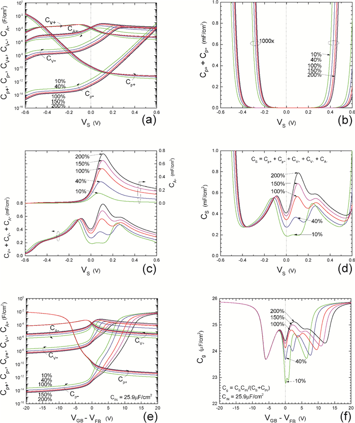
More than 80 years of theories and experiments on water suggested to us, described in our first water-physics report, that pure water's "abnormally" high electrical conductivity is due to transport of positive and negative quasi-protons, p+ and p-, between the neutral proton traps V0 ≡ (H2O)0 in the extended water, [(H2O)N→∞]0±, converting it respectively to positively and negatively charged proton traps, V+ ≡ (H3O)1+ and V- ≡ (HO)1-. In this second report, we present the theoretical charge control capacitances of pure and impure water as a function of the DC electric potential applied to water.
Issue Browser
Volume 35, Issue 2,
Feb 2014


J. Semicond.
2014, 35(2): 023001 doi: 10.1088/1674-4926/35/2/023001
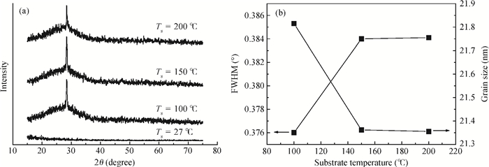
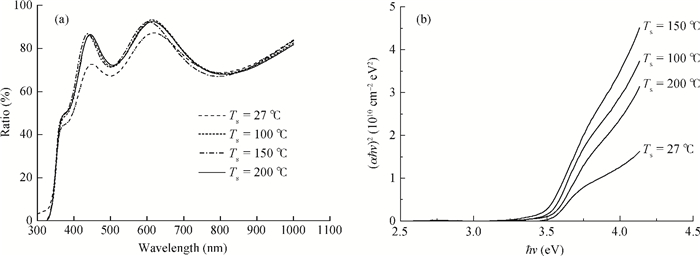
Indium doped ZnS (ZnS:In) films were prepared on glass substrate by using thermal evaporation technology. It was found that the structural, optical and electrical properties of ZnS:In films strongly depend on the substrate temperature (Ts). By utilizing X-ray diffraction (XRD), atomic force microscopy (AFM), transmittance spectroscopy, and electric performance measurements, the effect of Ts on ZnS:In film is studied in detail. It reveals that Ts has important effect on ZnS grain size, crystallinity, lattice disorder, etc., which further leads to the obvious influence on its optical and electrical performance. Under the optimized Ts, the performance, especially the conductivity, achieved in this work is far higher than that reported for other n-type ZnS films.


J. Semicond.
2014, 35(2): 023002 doi: 10.1088/1674-4926/35/2/023002
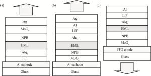
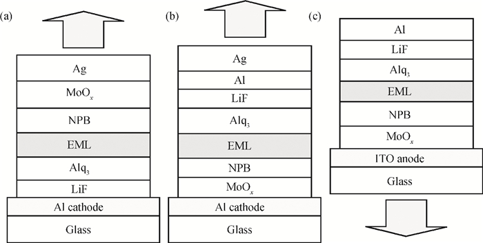
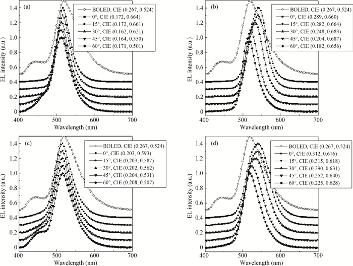
We demonstrate a highly efficient inverted top-emitting organic light-emitting diode (TOLED) having stable electroluminescent spectra and color coordination with variation of viewing angles by simply tuning the resonance wavelength corresponding to the free emission of the emitter. Using a doped fluorescent emitting system, the inverted TOLED exhibits an enhanced maximum current efficiency of 19 cd/A and a power efficiency of 17 lm/W, which are much higher than those (11 cd/A and 5 lm/W) of the counterpart with normal structure, although both TOLEDs behave with similar stable electroluminescent spectra characteristics. The results indicate that we provide a simple and effective method of constructing an excellent inverted TOLED for potentially practical applications.
J. Semicond.
2014, 35(2): 024001 doi: 10.1088/1674-4926/35/2/024001

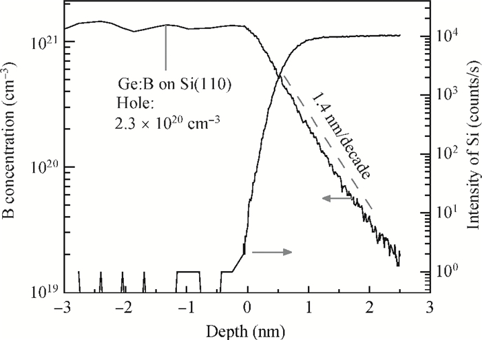
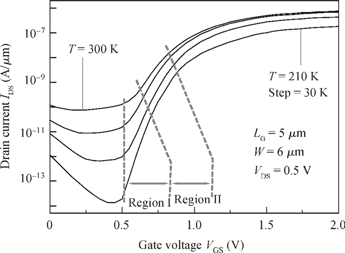
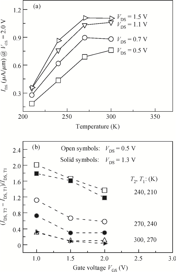
We fabricated n-type Si-based TFETs with a Ge source on Si(110) substrate. The temperature dependent IDS-VGS characteristics of a TFET formed on Si(110) are investigated in the temperature range of 210 to 300 K. A study of the temperature dependence of $I_{\rm Leakage}$ indicates that $I_{\rm Leakage}$ is mainly dominated by the Shockley-Read-Hall (SRH) generation-recombination current of the n+ drain-Si substrate junction. $I_{\rm ON}$ increases monotonically with temperature, which is attributed to a reduction of the bandgap at the tunneling junction and an enhancement of band-to-band tunneling rate. The subthreshold swing S for trap assisted tunneling (TAT) current and band-to-band tunneling (BTBT) current shows the different temperature dependence. The subthreshold swing S for the TAT current degrades with temperature, while the S for BTBT current is temperature independent.


J. Semicond.
2014, 35(2): 024002 doi: 10.1088/1674-4926/35/2/024002
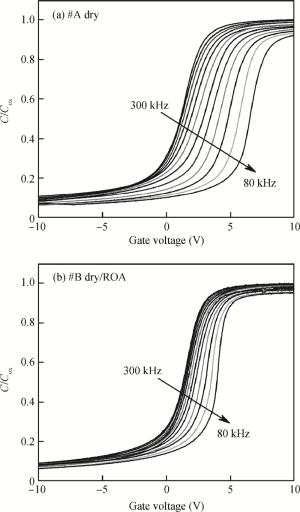
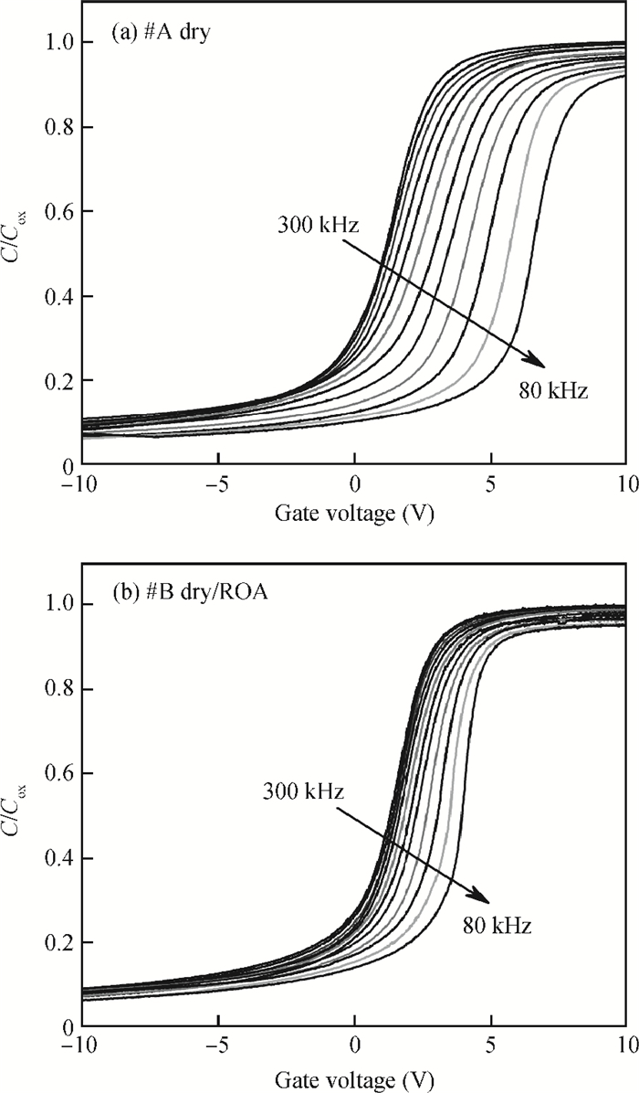
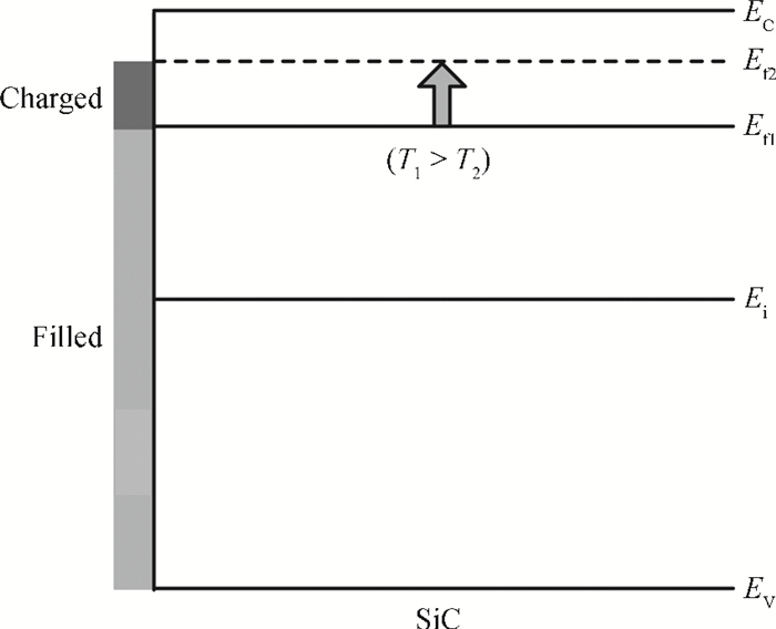
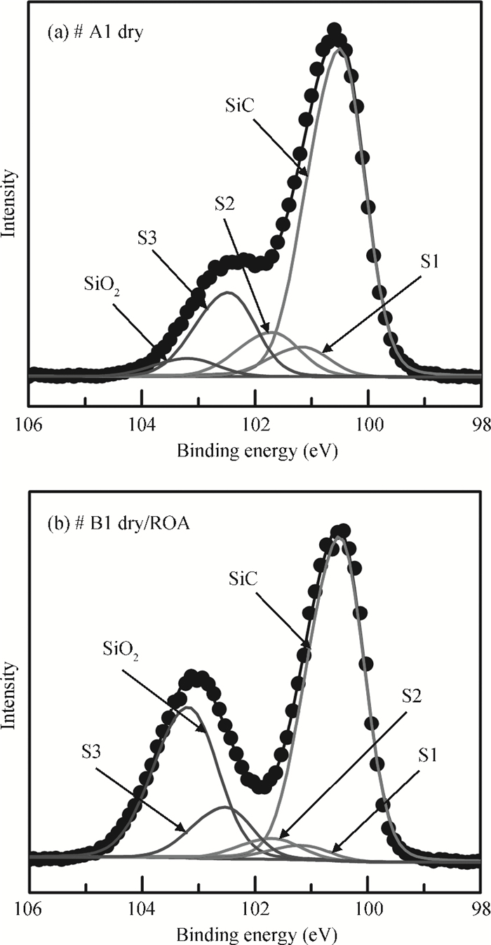
The effects of wet re-oxidation annealing (wet-ROA) on the shallow interface traps of n-type 4H-SiC metal-oxide-semiconductor (MOS) capacitors were investigated by Gray-Brown method and angle-dependent X-ray photoelectron spectroscopy technique. The results present the energy distribution of the density of interface traps ($D_{\rm it})$ from 0 to 0.2 eV below SiC conduction band edge ($E_{\rm C})$ of the sample with wet-ROA for the first time, and indicate that wet-ROA could reduce the $D_{\rm it}$ in this energy range by more than 60%. The reduction in $D_{\rm it}$ is attributed to the reaction between the introduced oxygen and the SiO$_{x}$C$_{y}$ species, which results in C release and SiO$_{x}$C$_{y}$ transformation into higher oxidation states, thus reducing the SiO$_{x}$C$_{y}$ content and the SiO$_{x}$C$_{y}$ interface transition region thickness.

J. Semicond.
2014, 35(2): 024003 doi: 10.1088/1674-4926/35/2/024003
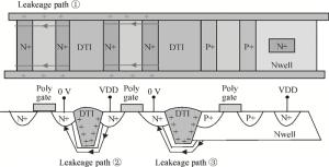
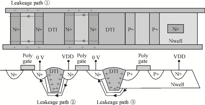
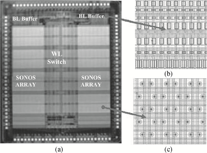
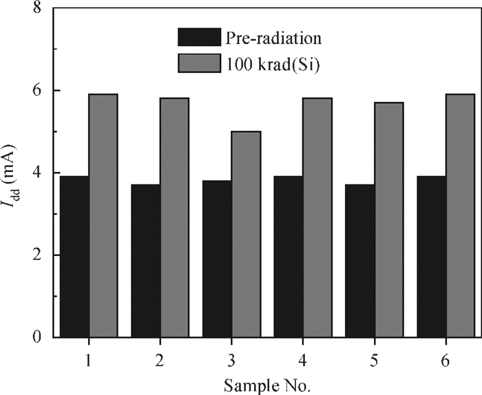
In order to minimize leakage current increase under total ionizing dose (TID) radiation in high density memory circuits, a new isolation technique, combining deep trench isolation (DTI) between the wells, local oxidation of silicon (LOCOS) isolation between the devices within the well, and a P-diffused area in order to limit leakage at the isolation edge is implemented in partly-depleted silicon-on-insulator (PD-SOI) technology. This radiation hardening technique can minimize the layout area by more than 60%, and allows flexible placement of the body contact. Radiation hardened transistors and 256 Kb flash memory chips are designed and fabricated in a 0.6 μm PD-SOI process. Experiments show that no obvious increase in leakage current is observed for single transistors under 1 Mrad(Si) radiation, and that the 256 Kb memory chip still functions well after a TID of 100 krad(Si), with only 50% increase of the active power consumption in read mode.


J. Semicond.
2014, 35(2): 024004 doi: 10.1088/1674-4926/35/2/024004
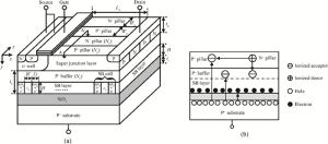
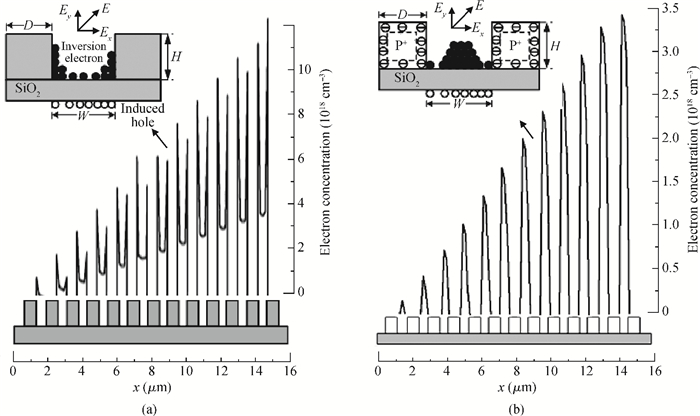
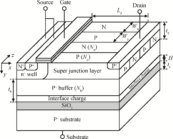
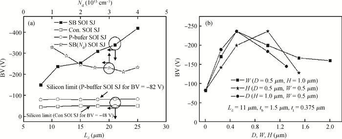
A new SOI self-balance (SB) super-junction (SJ) pLDMOS with a self-adaptive charge (SAC) layer and its physical model are presented. The SB is an effective way to realize charges balance (CB). The substrate-assisted depletion (SAD) effect of the lateral SJ is eliminated by the self-adaptive inversion electrons provided by the SAC. At the same time, high concentration dynamic self-adaptive electrons effectively enhance the electric field (EI) of the dielectric buried layer and increase breakdown voltage (BV). EI=600 V/μm and BV=-237 V are obtained by 3D simulation on a 0.375-μm-thick dielectric layer and a 2.5-μm-thick top silicon layer. The optimized structure realizes the specific on resistance (Ron, sp) of 0.01319 Ω·cm2, FOM (FOM=BV2/Ron, sp) of 4.26 MW/cm2 under a 11 μm length (Ld) drift region.


J. Semicond.
2014, 35(2): 024005 doi: 10.1088/1674-4926/35/2/024005
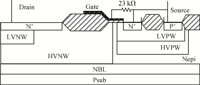
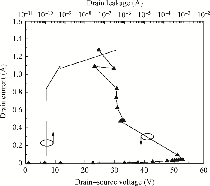
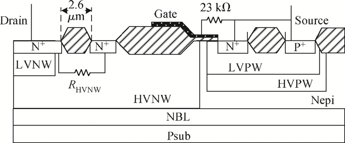
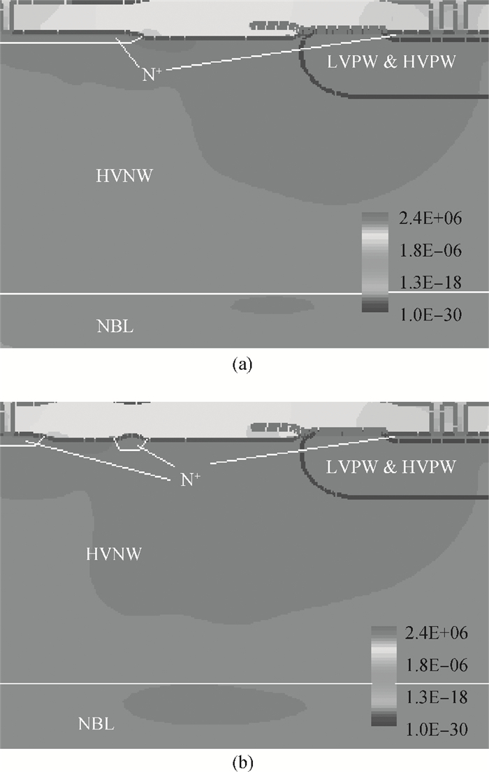
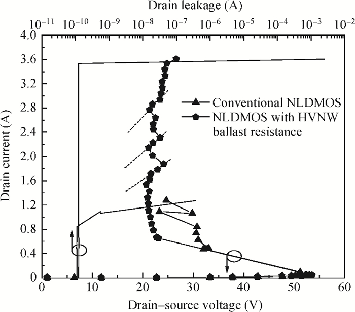
To prevent the non-uniform conduction phenomenon caused by the Kirk effect in an NLDMOS under ESD stress, a novel NLDMOS structure is proposed. High electron injection current is the base of Kirk effect. Higher electron injection can makes the Kirk effect more serious and lead easily to the non-uniform conduction phenomenon. By splitting the drain N+ with the field oxide in the proposed structure, the crowded current can lead to a higher voltage drop on the ballast resistance. Therefore, the non-uniform conduction is suppressed, and its failure current is much improved.


J. Semicond.
2014, 35(2): 024006 doi: 10.1088/1674-4926/35/2/024006
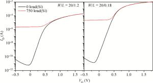
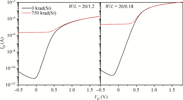
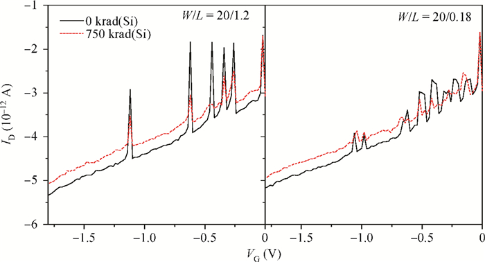
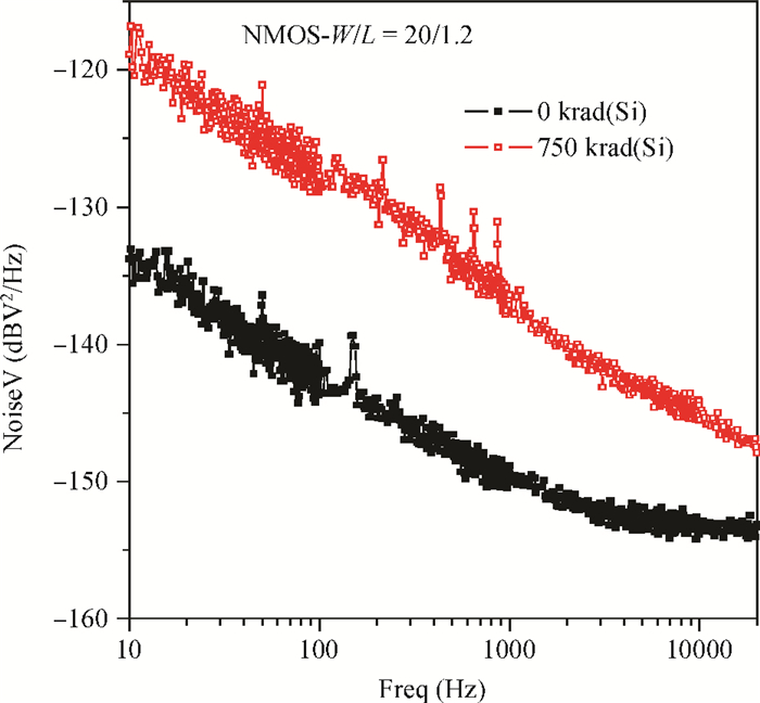
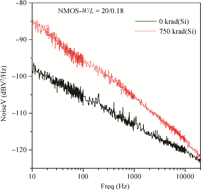
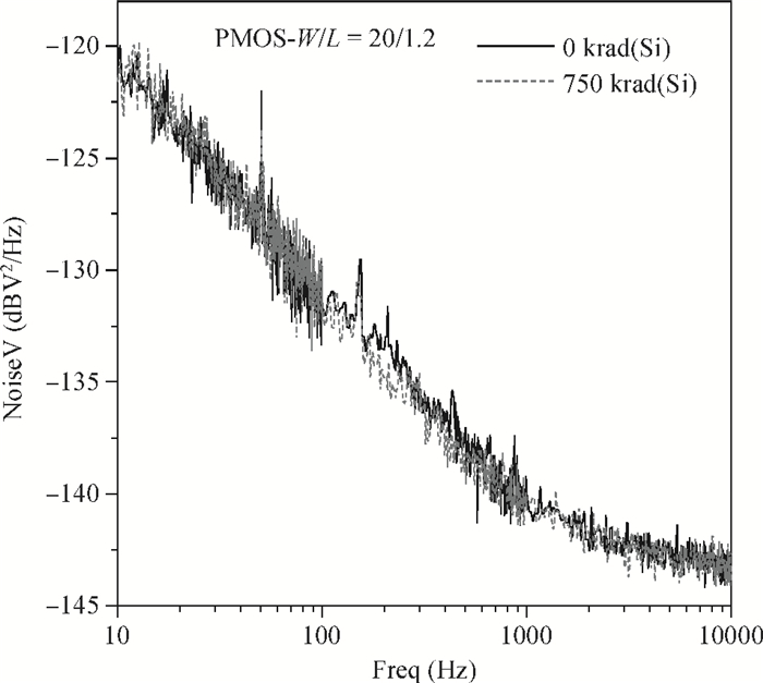
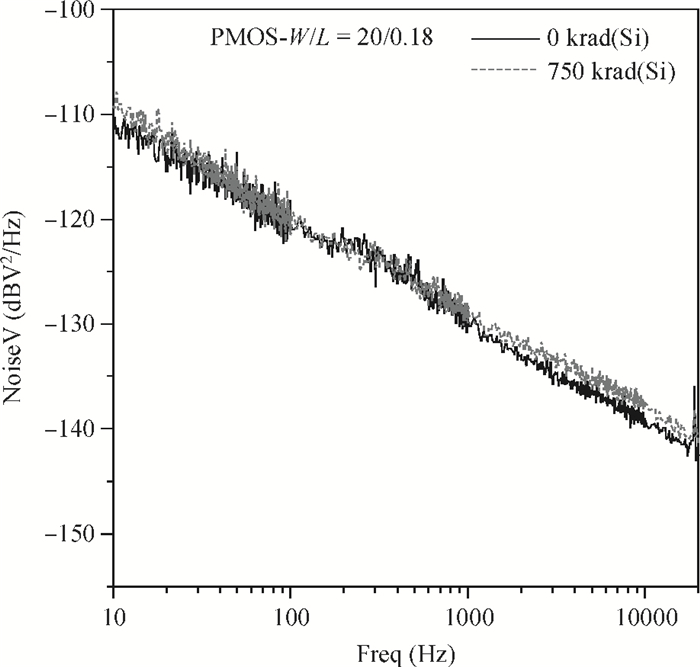
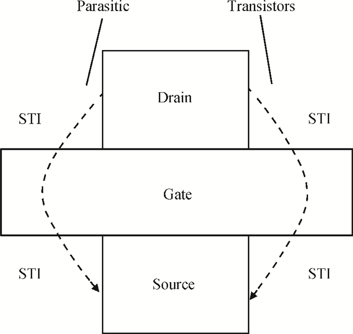
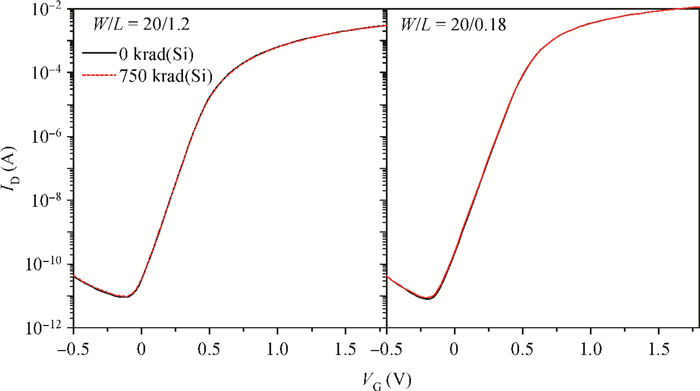
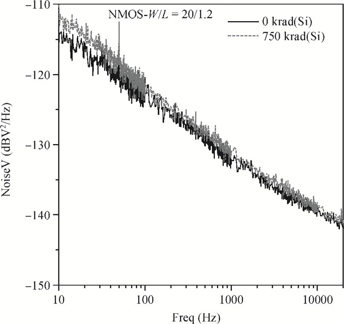
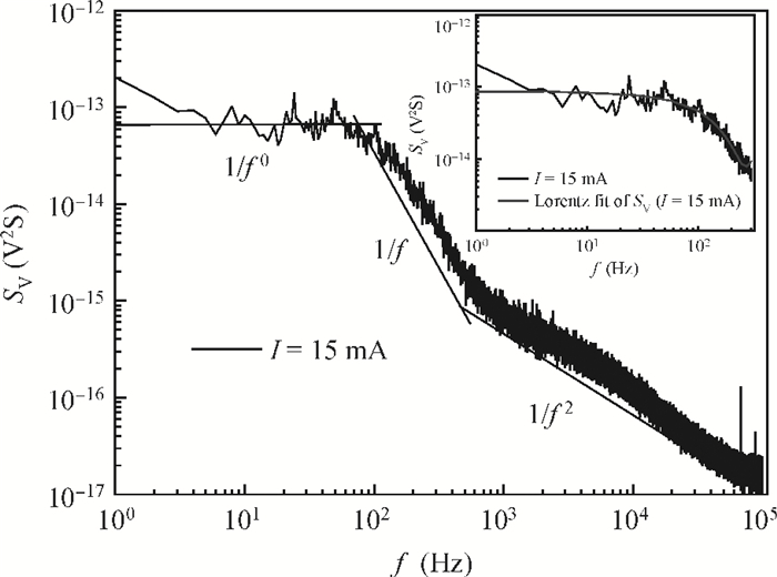
Using 0.18 μm CMOS transistors, the total dose effects on the 1/f noise of deep-submicron CMOS transistors are studied for the first time in mainland China. From the experimental results and the theoretic analysis, we realize that total dose radiation causes a lot of trapped positive charges in STI (shallow trench isolation) SiO2 layers, which induces a current leakage passage, increasing the 1/f noise power of CMOS transistors. In addition, we design some radiation-hardness structures on the CMOS transistors and the experimental results show that, until the total dose achieves 750 krad, the 1/f noise power of the radiation-hardness CMOS transistors remains unchanged, which proves our conclusion.


J. Semicond.
2014, 35(2): 024007 doi: 10.1088/1674-4926/35/2/024007
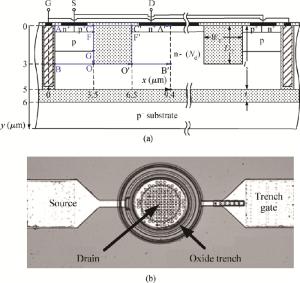
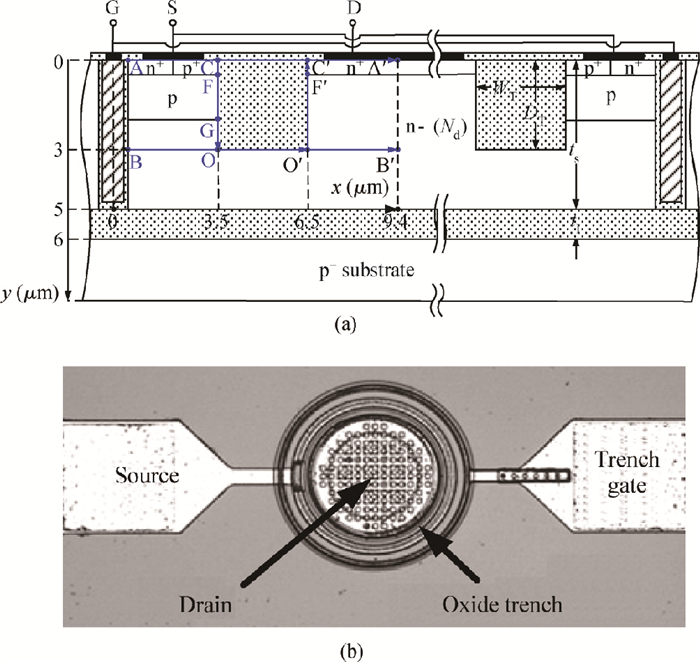
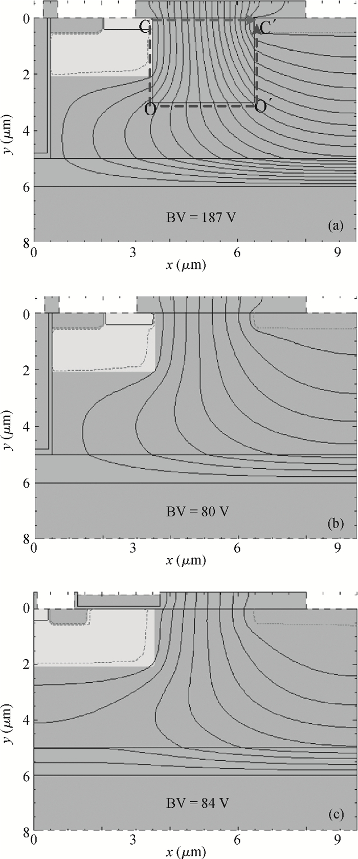
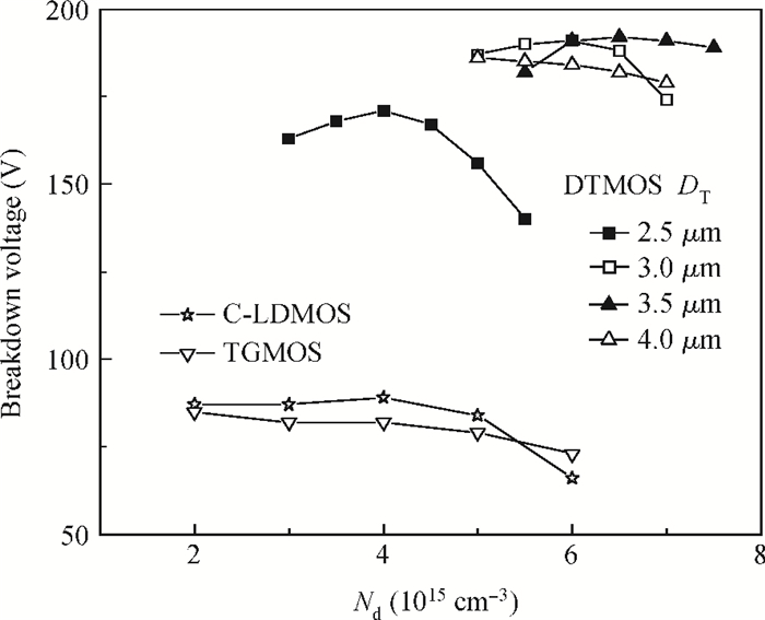
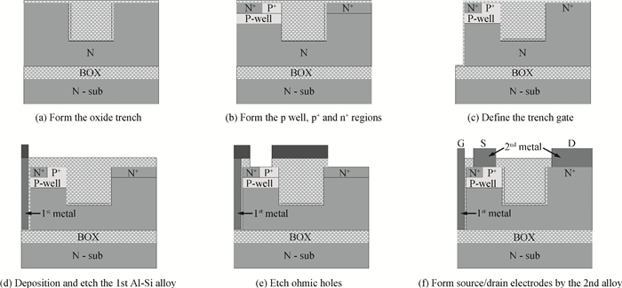
An improved breakdown voltage (BV) SOI power MOSFET with a reduced cell pitch is proposed and fabricated. Its breakdown characteristics are investigated numerically and experimentally. The MOSFET features dual trenches (DTMOS), an oxide trench between the source and drain regions, and a trench gate extended to the buried oxide (BOX). The proposed device has three merits. First, the oxide trench increases the electric field strength in the x-direction due to the lower permittivity of oxide (εox) than that of Si (εSi). Furthermore, the trench gate, the oxide trench, and the BOX cause multi-directional depletion, improving the electric field distribution and enhancing the RESURF (reduced surface field) effect. Both increase the BV. Second, the oxide trench folds the drift region along the y-direction and thus reduces the cell pitch. Third, the trench gate not only reduces the on-resistance, but also acts as a field plate to improve the BV. Additionally, the trench gate achieves the isolation between high-voltage devices and the low voltage CMOS devices in a high-voltage integrated circuit (HVIC), effectively saving the chip area and simplifying the isolation process. An 180 V prototype DTMOS with its applied drive IC is fabricated to verify the mechanism.


J. Semicond.
2014, 35(2): 024008 doi: 10.1088/1674-4926/35/2/024008
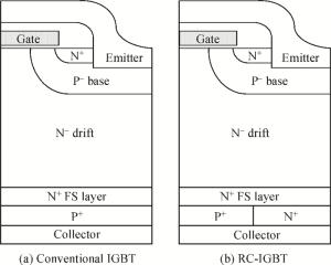
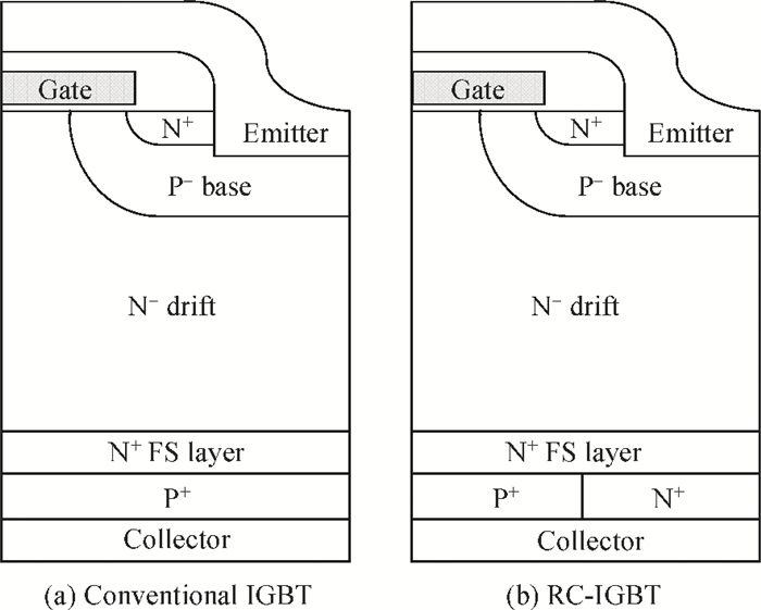
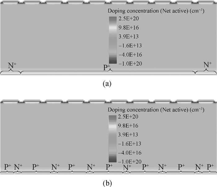
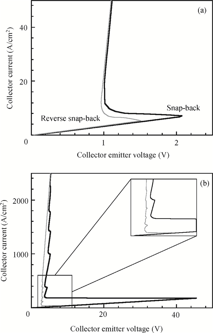
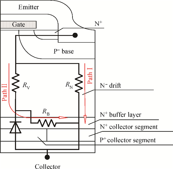
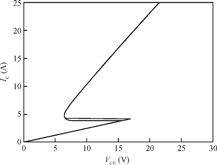
A simple equivalent circuit model is proposed according to the device structure of reverse conducting insulated gate bipolar transistors (RC-IGBT). Mathematical derivation and circuit simulations indicate that this model can explain the snap-back effect (including primary snap-back effect, secondary snap-back effect, and reverse snap-back effect) and hysteresis effect perfectly.

Correlation between dark current RTS noise and defects for AlGaInP multiple-quantum-well laser diode
J. Semicond.
2014, 35(2): 024009 doi: 10.1088/1674-4926/35/2/024009
The correlation model between dark current RTS noise and defects for AlGaInP multiple-quantum-well laser diode is derived. Experimental results show that dark current RTS noise caused carrier number fluctuations at the interface of the heterojunction in the active region. According to this correlation model, the defect types are determined, and the defects' energy levels are quantitatively determined. The corner frequency of RTS noise power spectral density is analyzed. The experimental results are in good agreement with the theoretical. This result provided an effective method for estimating the deep-level traps in the active region of AlGaInP multiple quantum well laser diode.
J. Semicond.
2014, 35(2): 024010 doi: 10.1088/1674-4926/35/2/024010
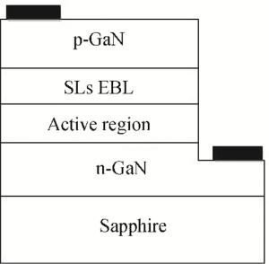
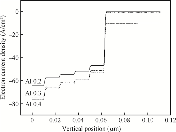
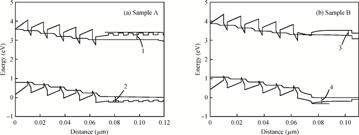
The advantages of the p-AlInGaN/GaN superlattices' (SLs) structure as an electron blocking layer (EBL) for InGaN blue light-emitting diodes (LEDs) were studied by experiment and APSYS simulation. Electroluminescence (EL) measurement results show that the LEDs with the p-AlInGaN/GaN SLs' structure EBL exhibited better optical performance compared with the conventional AlGaN EBL due to the enhancement of hole concentration and hole carrier transport efficiency, and the confinement of electrons' overflow between multiple quantum-wells (MQWs) and EBL.


J. Semicond.
2014, 35(2): 024011 doi: 10.1088/1674-4926/35/2/024011
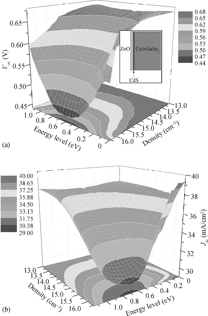
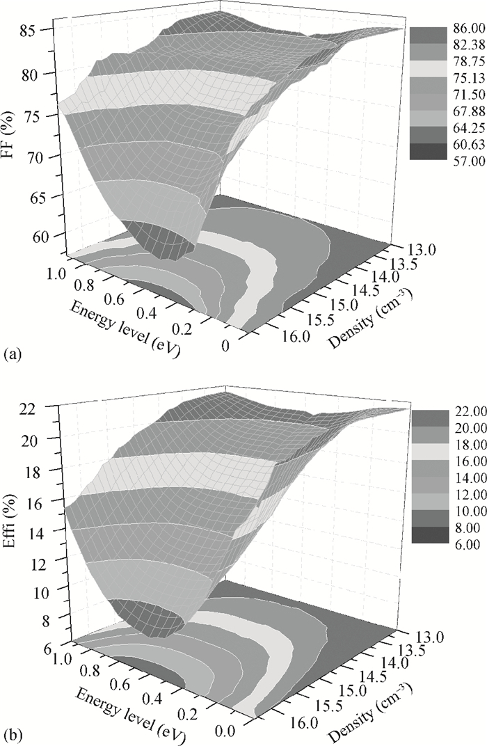
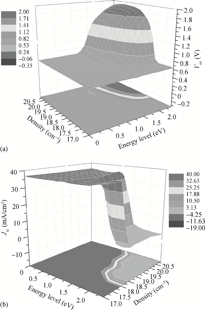
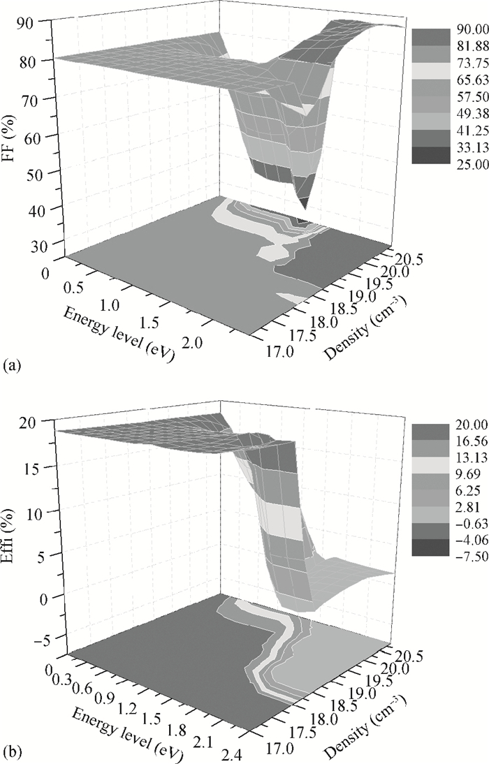
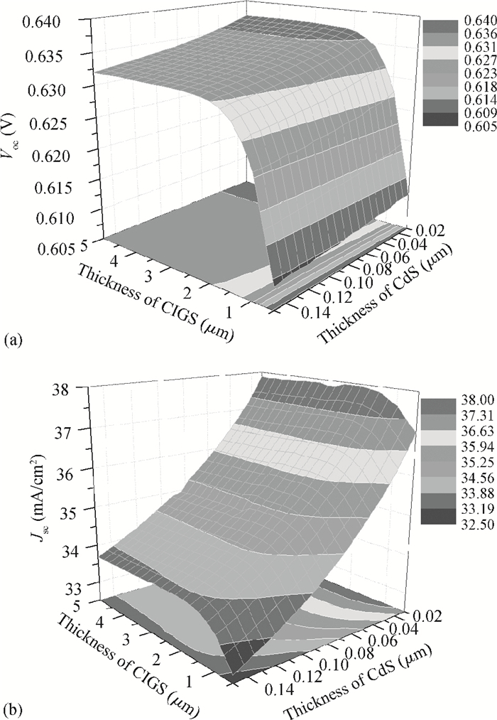
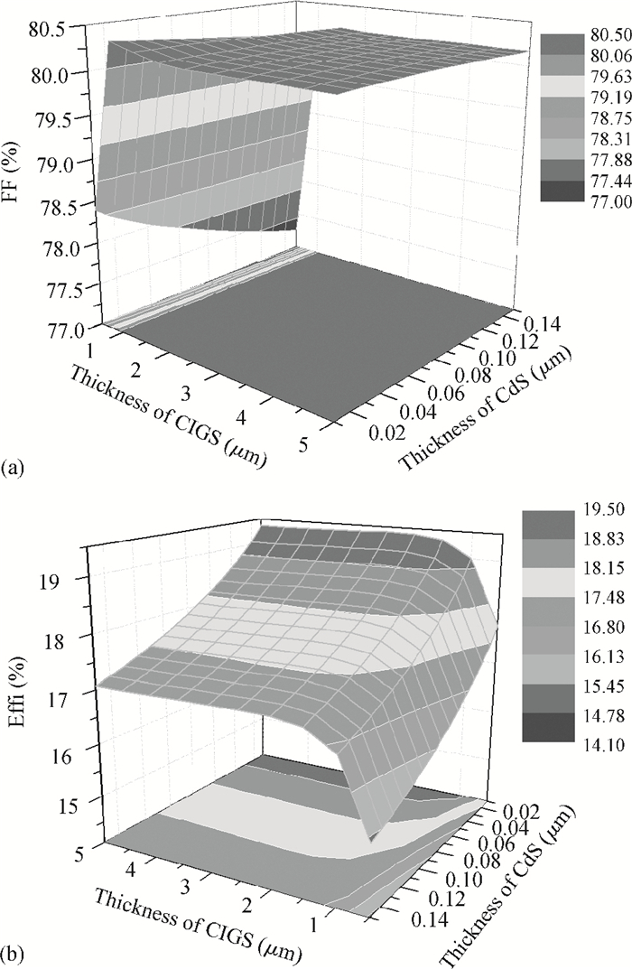
Device modeling has been carried out to investigate the effects of defect states on the performance of ideal CuInGaSe2 (CIGS) thin film solar cells theoretically. The varieties of defect states (location in the band gap and densities) in absorption layer CIGS and in buffer layer CdS were examined. The performance parameters:open-circuit voltage, short-circuit current, fill factor, and photoelectric conversion efficiency for different defect states were quantitatively analyzed. We found that defect states always harm the performance of CIGS solar cells, but when defect state density is less than 1014 cm-3 in CIGS or less than 1018 cm-3 in CdS, defect states have little effect on the performances. When defect states are located in the middle of the band gap, they are more harmful. The effects of temperature and thickness are also considered. We found that CIGS solar cells have optimal performance at about 170 K and 2 μm of CIGS is enough for solar light absorption.


J. Semicond.
2014, 35(2): 024012 doi: 10.1088/1674-4926/35/2/024012
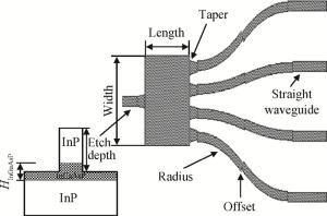
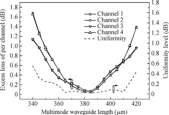
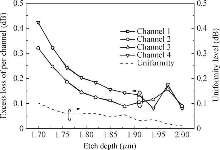
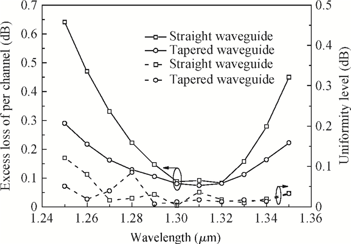
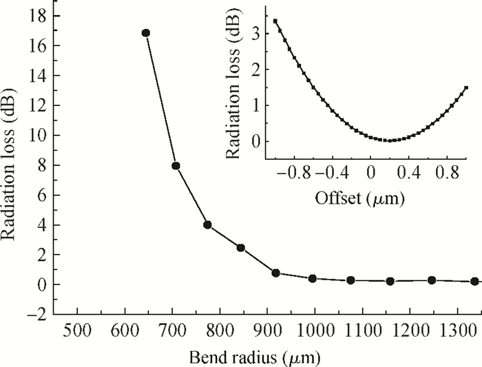
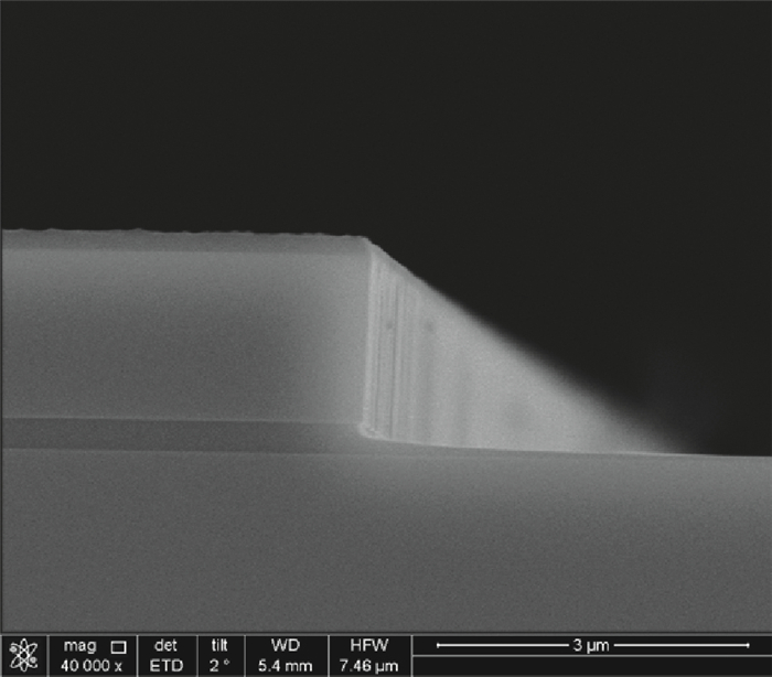
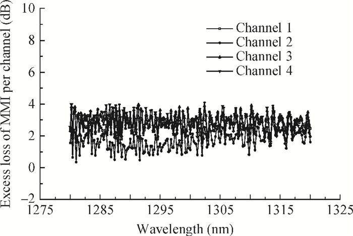
A 1.3-μm 1×4 MMI coupler is designed and fabricated on an InP substrate based on a shallow etched waveguide structure. Tapered input/output waveguides and a bending waveguide design are adopted and applied in the device to optimize the performance. The average excess losses of the 1×4 MMI coupler per channel are 2.8, 1.7, 2.9, and 2.9 dB, respectively. The smallest excess loss can be lower than 0.5 dB in the 40-nm spectrum bandwidth. The average uniformity between the four channels of the MMI coupler is 1.3 dB, while the smallest uniformity is only 0.4 dB.


J. Semicond.
2014, 35(2): 024013 doi: 10.1088/1674-4926/35/2/024013
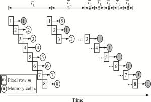
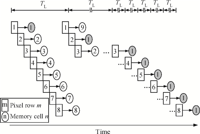
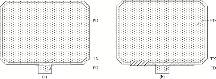
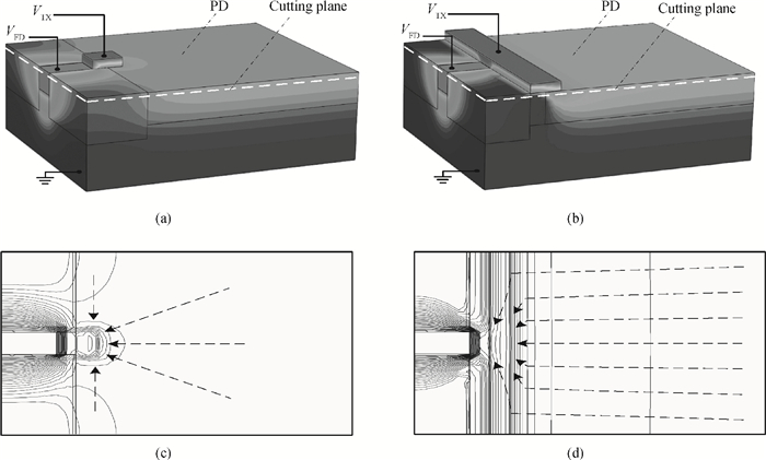
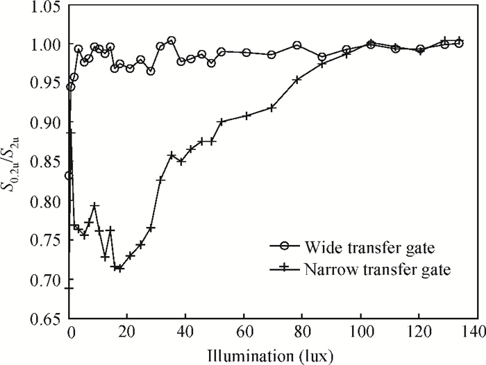
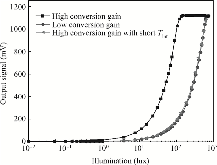
A dynamic range extension scheme applied to a time delay integration (TDI) CMOS image sensor (CIS) is presented. Two types of pixels with higher and lower conversion gain are adopted in the pixel array, which are suitable for capturing images in low and high illumination respectively. By fusing the two kinds of pixels' output signals in the process of TDI accumulation, a high dynamic range image can be achieved. Compared with the traditional multiple integration technique, no photoelectrons generated during the exposure time are discarded by the reset operation, and thus a higher level of signal-to-noise ratio (SNR) can be retained. A prototype chip with an 8×8 pixel array is implemented in a 0.18 μm CIS process, and the pixel size is 15×15 μm2. Test results show that a 76 dB dynamic range can be achieved in 8-stage TDI mode, when the SNR boost can reach 7.26 dB at 90.8 lux.


J. Semicond.
2014, 35(2): 025001 doi: 10.1088/1674-4926/35/2/025001
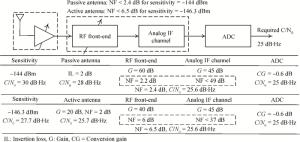
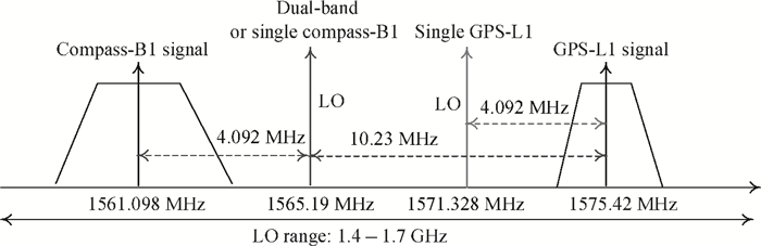
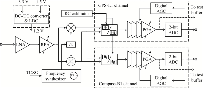
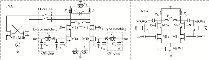
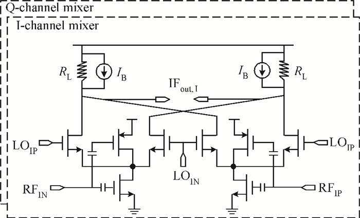
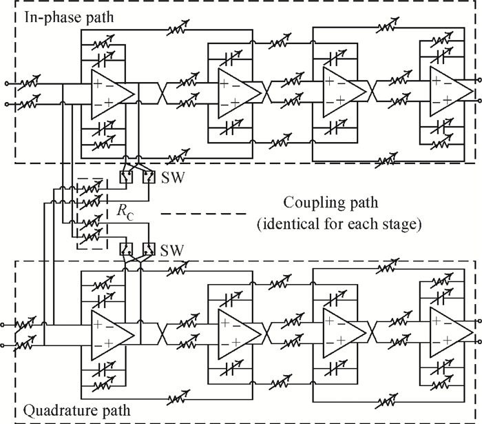
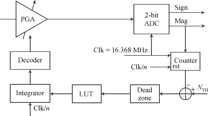
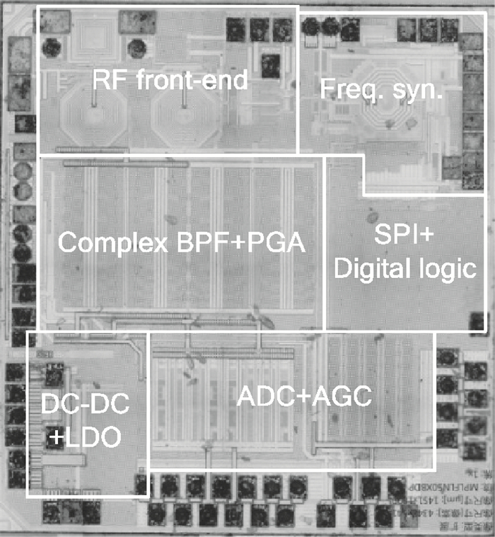
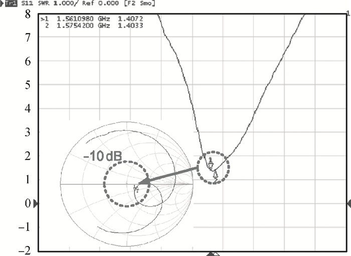
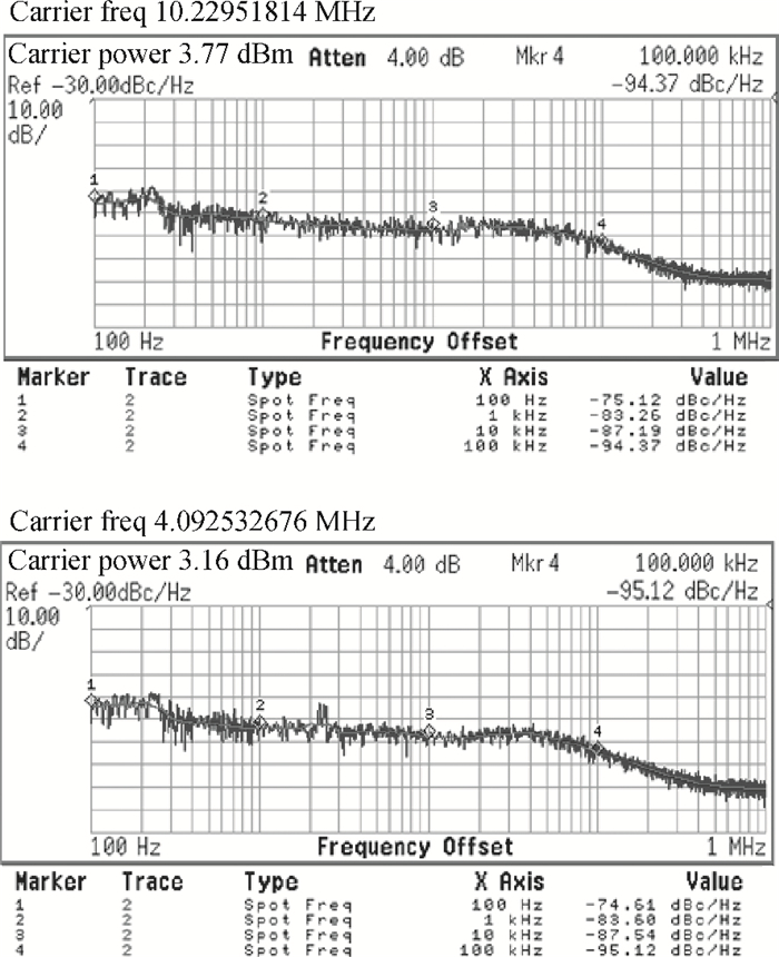
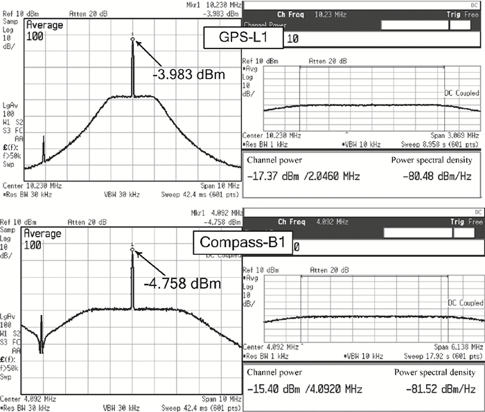
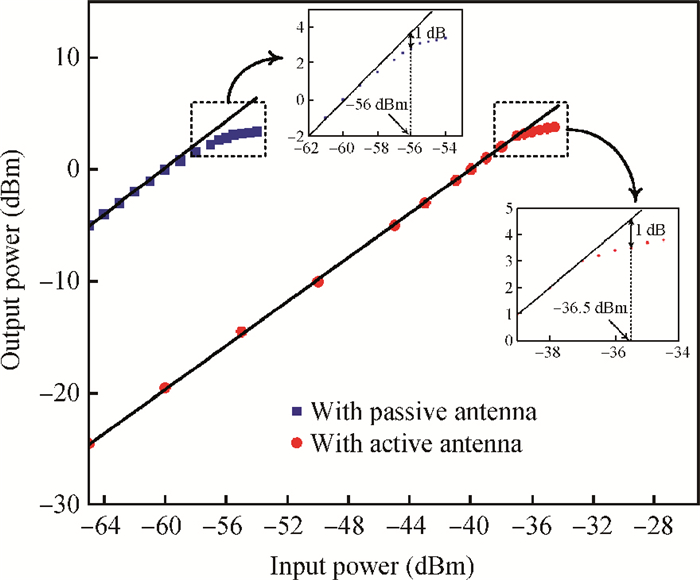
A fully integrated dual-band RF receiver with a low-IF architecture is designed and implemented for GPS-L1 and Compass-B1 in a 55-nm CMOS process. The receiver incorporates two independent IF channels with 2 or 4 MHz bandwidth to receive dual-band signals around 1.57 GHz respectively. By implementing a flexible frequency plan, the RF front-end and frequency synthesizer are shared for the dual-band operation to save power consumption and chip area, as well as avoiding LO crosstalk. A digital automatic gain control (AGC) loop is utilized to improve the receiver's robustness by optimizing the conversion gain of the analog-to-digital converter (ADC). While drawing about 20 mA per channel from a 1.2 V supply, this RF receiver achieves a minimum noise figure (NF) of about 1.8 dB, an image rejection (IMR) of more than 35 dB, a maximum voltage gain of about 122 dB, a gain dynamic range of 82 dB, and an maximum input-referred 1 dB compression point of about -36.5 dBm with an active die area of 1.5×1.4 mm2 for the whole chip.


J. Semicond.
2014, 35(2): 025002 doi: 10.1088/1674-4926/35/2/025002
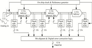
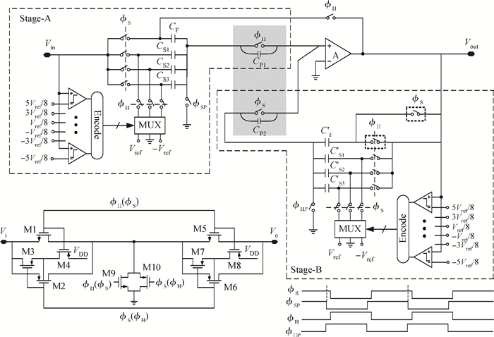
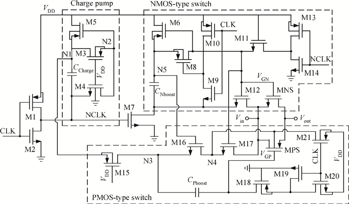
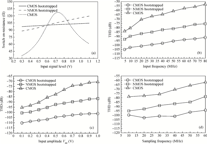
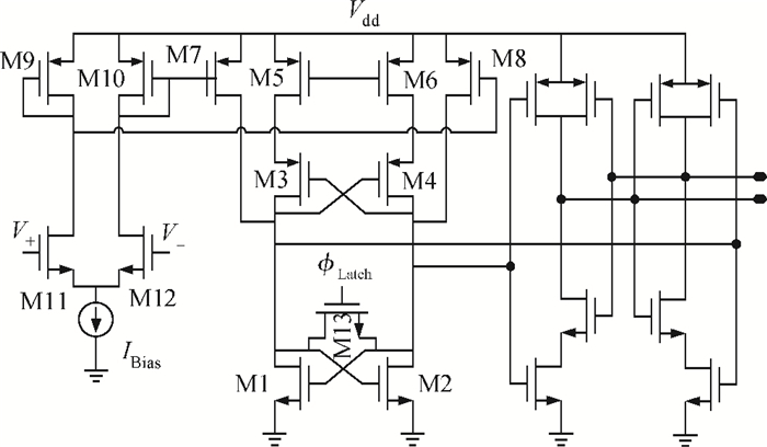
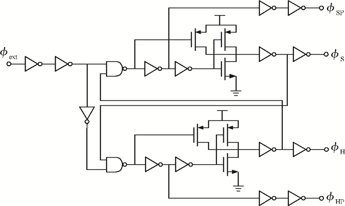
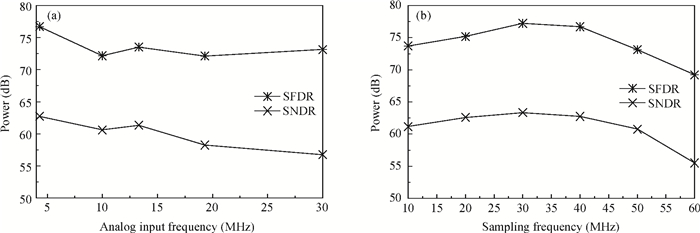
A power-efficient 12-bit 40-MS/s pipeline analog-to-digital converter (ADC) implemented in a 0.13 μm CMOS technology is presented. A novel CMOS bootstrapping switch, which offers a constant on-resistance over the entire input signal range, is used at the sample-and-hold front-end to enhance the dynamic performance of the pipelined ADC. By implementing with 2.5-bit-per-stage and a simplified amplifier sharing architecture between two successive pipeline stages, a very competitive power consumption and small die area can be achieved. Meanwhile, the substrate-biasing-effect attenuated T-type switches are introduced to reduce the crosstalk between the two op-amp sharing successive stages. Moreover, a two-stage gain boosted recycling folded cascode (RFC) amplifier with hybrid frequency compensation is developed to further reduce the power consumption and maintain the ADC's performance simultaneously. The measured results imply that the ADC achieves a spurious-free dynamic range (SFDR) of 75.7 dB and a signal-to-noise-plus-distortion ratio (SNDR) of 62.74 dB with a 4.3 MHz input signal; the SNDR maintains over 58.25 dB for input signals up to 19.3MHz. The measured differential nonlinearity (DNL) and integral nonlinearity (INL) are -0.43 to +0.48 LSB and -1.62 to +1.89 LSB respectively. The prototype ADC consumes 28.4 mW under a 1.2-V nominal power supply and 40 MHz sampling rate, transferring to a figure-of-merit (FOM) of 0.63 pJ per conversion-step.


J. Semicond.
2014, 35(2): 025003 doi: 10.1088/1674-4926/35/2/025003

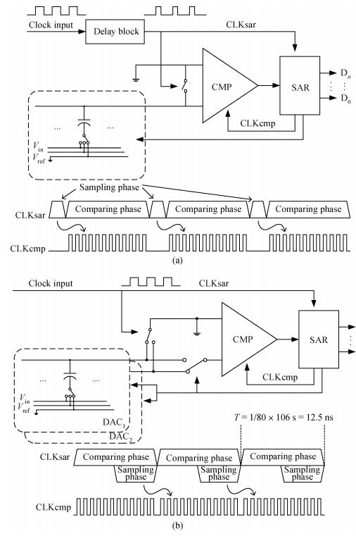
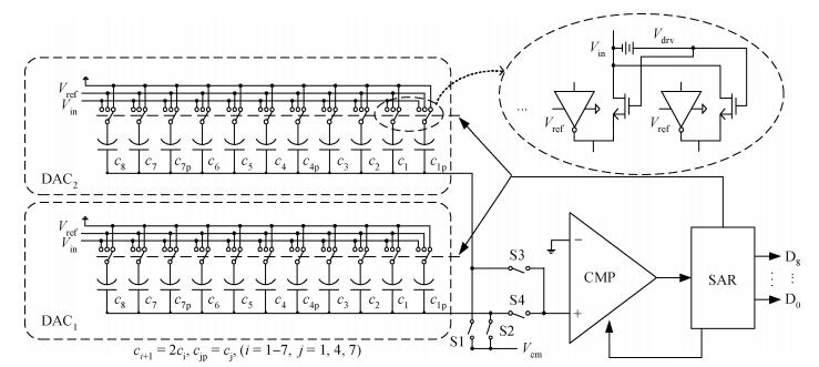
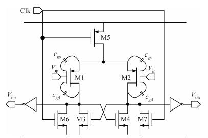
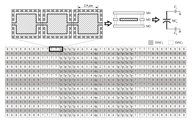
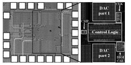
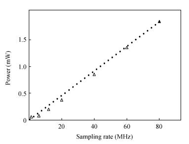
This paper presents a low power 9-bit 80 MS/s SAR ADC that uses the comparator-sharing technique in a 130 nm CMOS process. Compared to the conventional SAR ADC, the sampling phase is removed to reach the full efficiency of the comparator. Thus the conversion rate increases by about 20% and its sampling time is relaxed. The design does not use any static components to achieve a widely scalable conversion rate with a constant FOM. The floorplan of the capacitor network is custom-designed to suppress the gain mismatch between the two DACs. The 'set-and-down' switching procedure and a novel binary-search error compensation scheme are utilized to further speed up the SA bit-cycling operation. A very fast logic controller is proposed with a delay time of only 90 ps. At 1.2 V supply and 80 MS/s the ADC achieves an SNDR of 51.4 dB and consumes 1.86 mW, resulting in an FOM of 76.6 fJ/conversion-step. The ADC core occupies an active area of only 0.089 mm2.


J. Semicond.
2014, 35(2): 025004 doi: 10.1088/1674-4926/35/2/025004
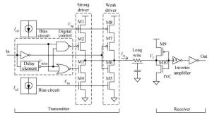
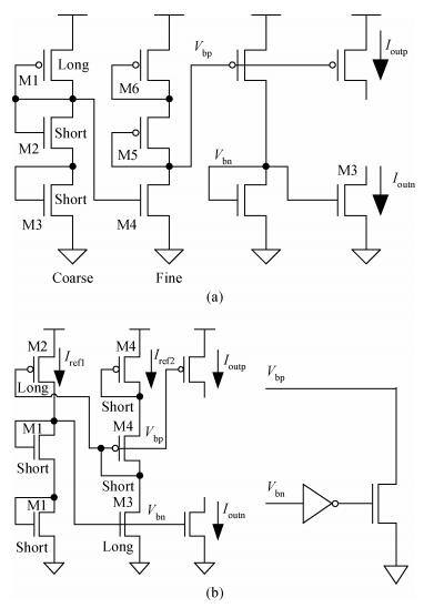
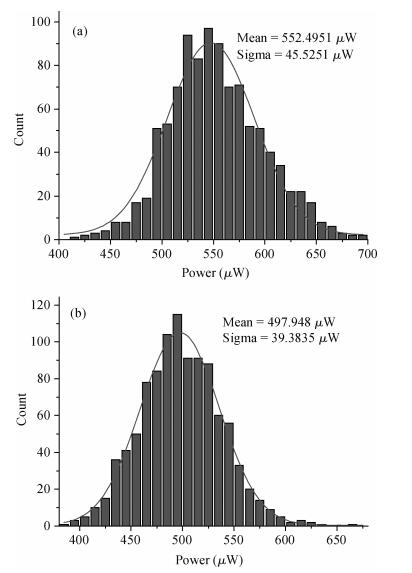
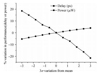
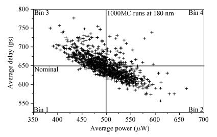
We propose a novel bias circuit, which can help a promising current-mode signaling (CMS) scheme (CMS-bias) enhance the robustness against process variation but consume less energy than the original bias circuit in this scheme. Monte Carlo and process corner analysis are carried out using HSPICE in the Global Foundry 0.18 μm process. Monte Carlo analysis shows that the CMS-bias with proposed bias circuit (CMS-proposed) and the CMS-bias with original circuit (CMS-original) have the same robustness against the variation, but the former offer a 9% reduction in power consumption. The process corner analysis shows that the average power and delay of the CMS-proposed don't change much in different process corners, especially in FS and SF corner. In addition, parameter sensitivity analysis shows that the process variation in long wires has little influence on the delay of the CMS scheme, but the variation in the effective length of MOSFETs influences the performance of the CMS scheme very much.


J. Semicond.
2014, 35(2): 025005 doi: 10.1088/1674-4926/35/2/025005

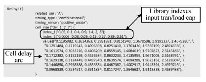
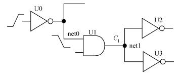
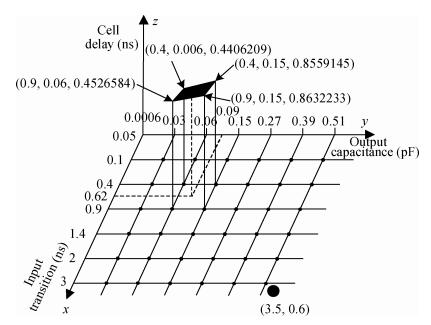
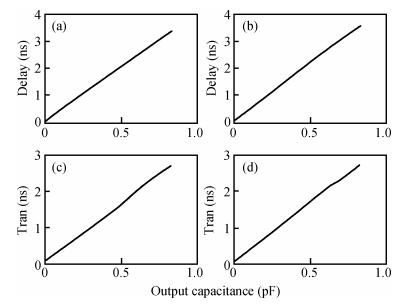
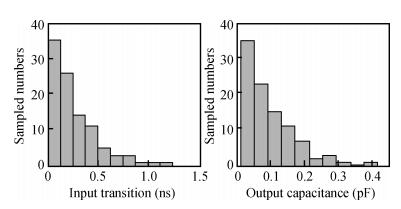
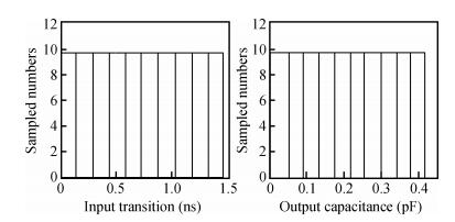
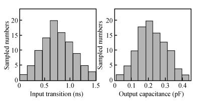
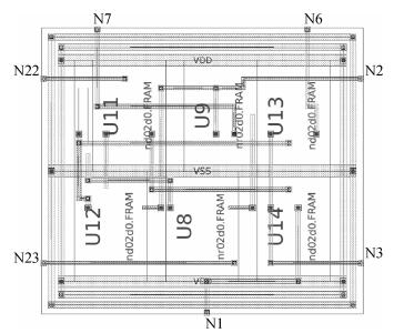
This paper presents a method of tailoring the characterization and modeling timing of a VLSI standard cell library. The paper also presents a method to validate the reasonability of the value through accuracy analysis. In the process of designing a standard cell library, this method is applied to characterize the cell library. In addition, the error calculations of some simple circuit path delays are compared between using the characterization file and an Hspice simulation. The comparison results demonstrate the accuracy of the generated timing library file.


J. Semicond.
2014, 35(2): 026001 doi: 10.1088/1674-4926/35/2/026001

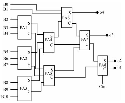
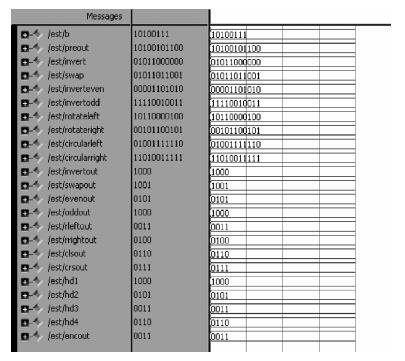
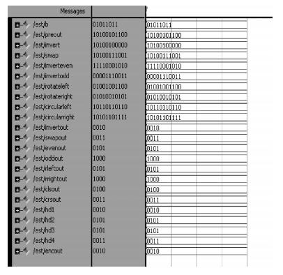
Advances in VLSI technology have enabled the implementation of complex digital circuits in a single chip, reducing system size and power consumption. In deep submicron low power CMOS VLSI design, the main cause of energy dissipation is charging and discharging of internal node capacitances due to transition activity. Transition activity is one of the major factors that also affect the dynamic power dissipation. This paper proposes power reduction analyzed through algorithm and logic circuit levels. In algorithm level the key aspect of reducing power dissipation is by minimizing transition activity and is achieved by introducing a data coding technique. So a novel multi coding technique is introduced to improve the efficiency of transition activity up to 52.3% on the bus lines, which will automatically reduce the dynamic power dissipation. In addition, 1 bit full adders are introduced in the Hamming distance estimator block, which reduces the device count. This coding method is implemented using Verilog HDL. The overall performance is analyzed by using Modelsim and Xilinx Tools. In total 38.2% power saving capability is achieved compared to other existing methods.


J. Semicond.
2014, 35(2): 026002 doi: 10.1088/1674-4926/35/2/026002
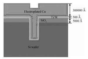
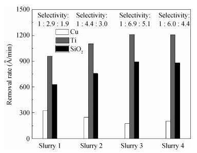
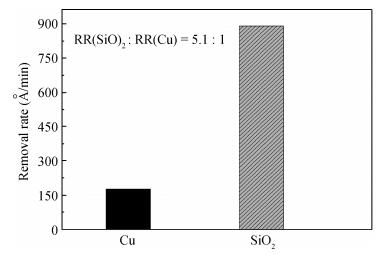
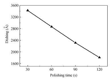
We have proposed a TSV (through-silicon-via) alkaline barrier slurry without any inhibitors for barrier CMP (chemical mechanical planarization) and investigated its CMP performance. The characteristics of removal rate and selectivity of Ti/SiO2/Cu were investigated under the same process conditions. The results obtained from 6.2 mm copper, titanium and silica show that copper has a low removal rate during barrier CMP by using this slurry, and Ti and SiO2 have high removal rate selectivity to Cu. Thus it may be helpful to modify the dishing. The TSV wafer results reveal that the alkaline barrier slurry has an obvious effect on surface topography correction, and can be applied in TSV barrier CMP.


J. Semicond.
2014, 35(2): 026003 doi: 10.1088/1674-4926/35/2/026003
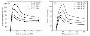
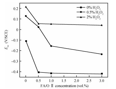
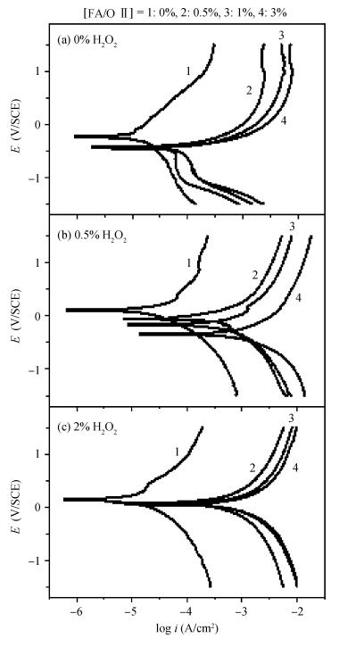
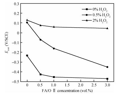
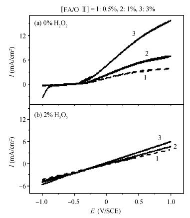
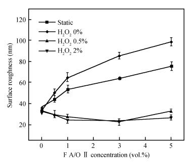
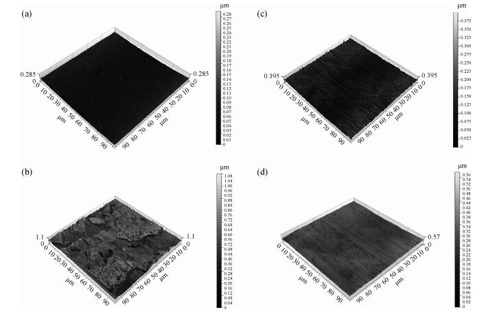
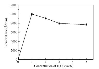
This work investigates the static corrosion and removal rates of copper as functions of H2O2 and FA/OⅡconcentration, and uses DC electrochemical measurements such as open circuit potential (OCP), Tafel analysis, as well as cyclic voltammetry (CV) to study H2O2 and FA/OⅡdependent surface reactions of Cu coupon electrode in alkaline slurry without an inhibitor. An atomic force microscopy (AFM) technique is also used to measure the surface roughness and surface morphology of copper in static corrosion and polishing conditions. It is shown that 0.5 vol.% H2O2 should be the primary choice to achieve high material removal rate. The electrochemical results reveal that the addition of FA/O Ⅱ can dissolve partial oxide film to accelerate the electrochemical anodic reactions and make the oxide layer porous, so that the structurally weak oxide film can be easily removed by mechanical abrasion. The variation of surface roughness and morphology of copper under static conditions is consistent with and provides further support for the reaction mechanisms proposed in the context of DC electrochemical measurements. In addition, in the presence of H2O2, 3 vol.% FA/O Ⅱ may be significantly effective from a surface roughness perspective to obtain a relatively flat copper surface in chemical mechanical planarization (CMP) process.

J. Semicond.
2014, 35(2): 026004 doi: 10.1088/1674-4926/35/2/026004
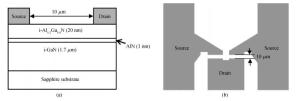
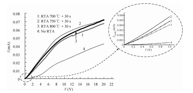
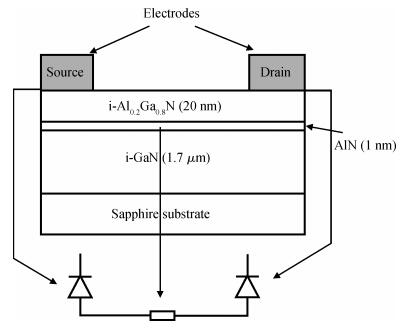
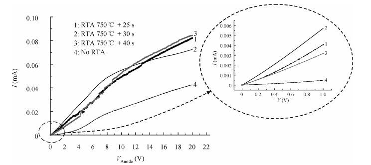
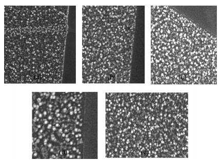
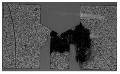
Ohmic contacts with Ti/Al/Ti/Au source and drain electrodes on AlGaN/GaN high electron mobility transistors (HEMTs) were fabricated and subjected to rapid thermal annealing (RTA) in flowing N2. The wafer was divided into 5 parts and three of them were annealed for 30 s at 700, 750, and 800℃, respectively, the others were annealed at 750℃ for 25 and 40 s. Due to the RTA, a change from Schottky contact to Ohmic contact has been obtained between the electrode layer and the AlGaN/GaN heterojunction layer. We have achieved a low specific contact resistance of 7.41×10⁻⁶ Ω·cm2 and contact resistance of 0.54 Ω·mm measured by transmission line mode (TLM), and good surface morphology and edge acuity are also desirable by annealing at 750℃ for 30 s. The experiments also indicate that the performance of ohmic contact is first improved, then it reaches a peak, finally degrading with annealing temperature or annealing time rising.

J. Semicond.
2014, 35(2): 026005 doi: 10.1088/1674-4926/35/2/026005

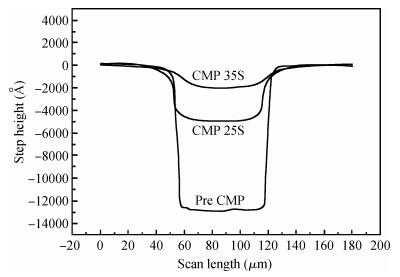
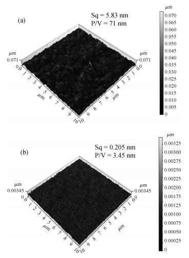
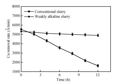
This study reports a new weakly alkaline slurry for copper chemical mechanical planarization (CMP), it can achieve a high planarization efficiency at a reduced down pressure of 1.0 psi. The slurry is studied through the polish rate, planarization, copper surface roughness and stability. The copper polishing experiment result shows that the polish rate can reach 10032 Å/min. From the multi-layers copper CMP test, a good result is obtained, that is a big step height (10870 Å) that can be eliminated in just 35 s, and the copper root mean square surface roughness (sq) is very low ( < 1 nm). Apart from this, compared with the alkaline slurry researched before, it has a good progress on stability of copper polishing rate, stable for 12 h at least. All the results presented here are relevant for further developments in the area of copper CMP.
J. Semicond.
2014, 35(2): 026006 doi: 10.1088/1674-4926/35/2/026006
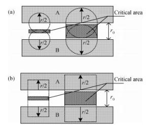
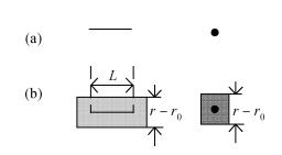
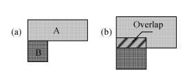
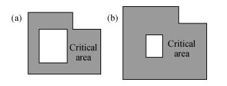
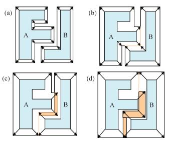
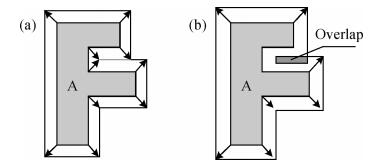
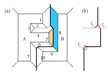
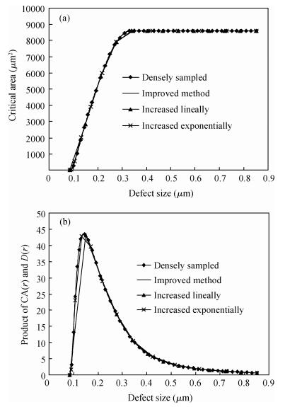
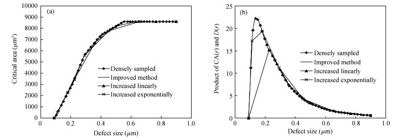
As die size and complexity increase, accurate and efficient extraction of the critical area is essential for yield prediction. Aiming at eliminating the potential integration errors of the traditional shape shifting method, an improved shape shifting method is proposed for Manhattan layouts. By mathematical analyses of the relevance of critical areas to defect sizes, the critical area for all defect sizes is modeled as a piecewise quadratic polynomial function of defect size, which can be obtained by extracting critical area for some certain defect sizes. Because the improved method calculates critical areas for all defect sizes instead of several discrete values with traditional shape shifting method, it eliminates the integration error of the average critical area. Experiments on industrial layouts show that the improved shape shifting method can improve the accuracy of the average critical area calculation by 24.3% or reduce about 59.7% computational expense compared with the traditional method.